
Can a Zigbee PCB Manufacturer Deliver Reliable RF Performance from Prototype to Mass Production?
A reliable Zigbee PCB depends on more than selecting a 2.4 GHz wireless chip. Antenna geometry, RF feed impedance, PCB stackup, grounding, component placement, soldering, enclosure materials, and production consistency all affect wireless performance. The right manufacturer must translate the approved RF design into a repeatable PCB and PCBA process, then validate the results against the product’s requirements.
What Is a Zigbee PCB and Which Products Use It?
A Zigbee PCB is a printed circuit board designed for an electronic product that uses Zigbee communication, typically based on IEEE 802.15.4. Its requirements depend on the selected wireless IC or module, antenna architecture, power budget, mechanical enclosure, and production volume.
Zigbee is commonly used in low-power wireless sensor networks, smart lighting, building automation, environmental monitoring, industrial monitoring, and connected control devices. The PCB may contain a Zigbee system-on-chip, a certified or prequalified wireless module, a discrete RF front end, an antenna, power-management circuits, sensors, and application-specific electronics.
For manufacturing purposes, a Zigbee PCB can fall into three broad categories:
| Product architecture | Typical PCB considerations | Main manufacturing risk |
|---|---|---|
| Wireless module on a host PCB | Module footprint, ground connections, power integrity, antenna keep-out | Host-board interference or incorrect antenna clearance |
| Integrated Zigbee RF circuit | RF feed, matching network, grounding, component placement | Layout variation affecting RF performance |
| Compact, multilayer Zigbee product | Dense routing, via placement, layer transitions, antenna isolation | Routing and mechanical constraints competing for space |
A module-based design can reduce the amount of RF circuitry that the product developer must design. However, it does not eliminate the need to follow the module manufacturer’s antenna, grounding, clearance, and enclosure requirements.
For example, Texas Instruments’ CC2530EM reference design documents PCB layout, stackup, RF decoupling, and balun-related considerations for a 2.4 GHz wireless design. These are practical reminders that the PCB implementation is part of the radio design, not simply a passive carrier. See the CC2530EM reference design.
When does the PCB architecture change the manufacturing plan?
Consider a compact battery-powered door sensor. The design may use a two-layer PCB or a compact multilayer board, depending on component density, antenna placement, and mechanical constraints. A larger industrial Zigbee gateway may require additional layers for power distribution, digital interfaces, shielding provisions, and routing density.
Neither product automatically needs an expensive high-frequency laminate. The correct stackup follows the electrical requirements and the validated reference design.
For compact products with dense routing, evaluate HDI PCB manufacturing only when the design genuinely benefits from finer routing, smaller capture pads, or microvia structures.
What Should Buyers Check When Choosing a Zigbee PCB Manufacturer?
Buyers should verify that the manufacturer can interpret the released PCB data, control critical fabrication variables, assemble the specified components, document inspection results, and support the required validation plan. A machine list alone does not demonstrate that a supplier can deliver repeatable Zigbee performance.
A supplier assessment should cover five areas.
| Evaluation area | Evidence to request | Why it matters |
|---|---|---|
| Engineering data review | Gerber or ODB++, drill files, stackup, fabrication notes | Prevents missing or contradictory manufacturing requirements |
| RF-sensitive fabrication | Finished copper, dielectric construction, controlled-impedance requirements where specified | Supports consistency of the intended RF transmission path |
| SMT assembly | Approved BOM, placement data, soldering process, inspection criteria | Reduces assembly defects around RF and power components |
| Electrical inspection | Electrical-test scope, acceptance criteria, test records | Detects manufacturing faults that visual inspection may miss |
| Production control | Approved revision, material traceability, process records, change control | Reduces variation between prototype and production batches |
Which manufacturing technologies can support a Zigbee PCB?
Shenzhen Hongda Circuit Technology Co., Ltd. uses manufacturing equipment including SCREEN Ledia laser direct imaging, Mitsubishi UV/CO₂ laser drilling, a LAUFFER lamination system, automated optical inspection, and X-ray inspection. The relevance of each technology depends on the actual board construction.
SCREEN Ledia laser direct imaging (LDI)
LDI images the circuit pattern directly rather than relying on a conventional phototool. This can help control pattern registration and fine-feature fabrication. It becomes more relevant when a Zigbee design uses dense SMT footprints, compact multilayer routing, or fine-pitch components.
Mitsubishi UV/CO₂ laser drilling
Laser drilling can form microvias for suitable multilayer and HDI constructions. It is not automatically necessary for a conventional two-layer Zigbee board. Its value increases when the design needs high routing density, compact dimensions, or specific interlayer connections.
LAUFFER vacuum lamination
Lamination control affects dielectric bonding, layer registration, and finished stackup consistency. For RF-sensitive boards, the relevant outcome is whether the finished construction matches the approved material and thickness requirements—not whether the board simply passed through a particular press.
Automated optical inspection (AOI) and X-ray inspection
AOI can detect visible circuit and assembly defects within its inspection scope. X-ray can help inspect hidden solder joints, such as certain bottom-terminated or ball-grid-array packages. Neither method independently confirms antenna efficiency, radio sensitivity, or wireless range.
The manufacturing equipment should therefore be evaluated against measurable acceptance criteria rather than presented as a guarantee of RF performance.
For applications requiring a more specific transmission-line or dielectric construction, review the relevant high-frequency PCB capabilities.
How Should a Zigbee PCB Antenna and RF Layout Be Designed?
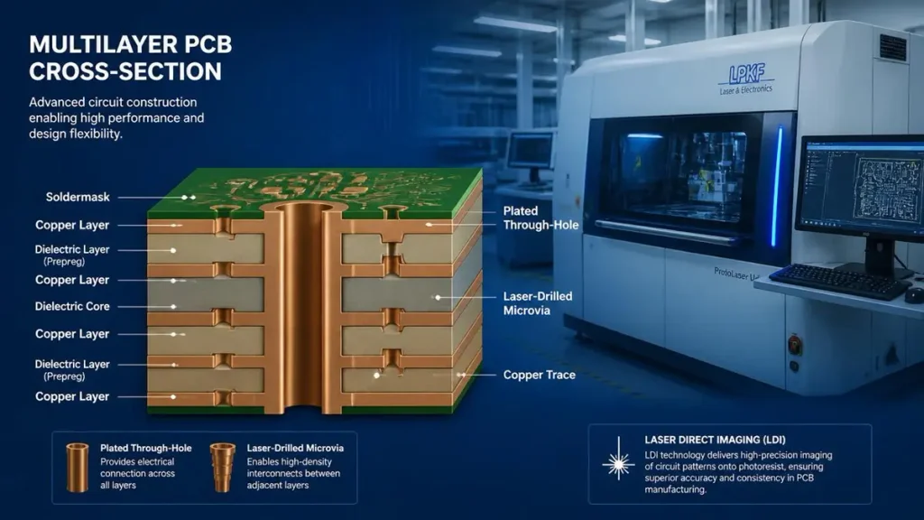
Zigbee PCB manufacturing with multilayer stackup, copper layers, LDI circuit imaging and microvia structures
The antenna and RF layout should follow the selected radio or module reference design, the actual PCB stackup, and the final product enclosure. Where the design specifies a 50 Ω RF feed, the manufacturer must work from the agreed impedance target and physical construction rather than applying a generic trace width.
Many Zigbee products operate in the 2.4 GHz band. At this frequency, small changes in the antenna region, ground plane, nearby components, dielectric construction, or enclosure can change antenna matching and radiation behavior.
The following parameters should be resolved during design review.
| Parameter | What the engineering team should specify | Why it matters |
|---|---|---|
| Operating frequency | The radio’s intended channel and frequency range | Establishes the RF design target |
| Antenna type | PCB antenna, chip antenna, or external antenna | Determines placement, matching, and clearance requirements |
| RF feed impedance | Target impedance, such as 50 Ω where required | Helps control reflections along the feed path |
| Stackup | Layer count, dielectric material, thickness, copper construction | Influences transmission-line behavior |
| Antenna keep-out | Exact restrictions from the antenna or module design | Reduces unwanted interaction with copper and components |
| Grounding | Ground-plane geometry, stitching vias, return-current path | Affects RF return paths and circuit behavior |
| Matching network | Approved circuit and component values, with tuning provisions where appropriate | Supports antenna matching and final integration |
| Mechanical environment | Enclosure, battery, cables, mounting hardware, nearby metal | These objects can detune the antenna or change radiation patterns |
Why can a Zigbee PCB pass electrical test but still have poor wireless range?
A continuity test confirms electrical connections within its test coverage. It does not establish that the antenna is correctly matched or that the completed product achieves its required radio performance.
For example, an OEM may approve a prototype with an exposed PCB antenna, then place the production board beside a metal battery holder or inside a plastic enclosure with different wall thickness. The board may still power up and communicate at short range, while the final product performs inconsistently at the intended operating distance.
A useful engineering investigation separates the potential causes:
- Fabrication: Verify the released stackup, copper pattern, relevant finished dimensions, and any specified impedance requirements.
- Assembly: Check the RF matching components, component orientation, solder joints, and unintended solder bridges.
- Integration: Evaluate the antenna in the actual enclosure with the intended battery, cables, and mounting hardware.
- RF validation: Measure the parameters required by the design, such as antenna matching, transmit behavior, receiver performance, and current consumption.
The exact test setup depends on the product. A VNA can help characterize antenna matching or a suitable RF structure, but it does not replace all radio-performance tests. Conducted measurements, radiated tests, or over-the-air tests may be required according to the product’s acceptance plan.
For a reference-design-based project, avoid changing the antenna geometry, matching network, or ground arrangement solely to make PCB routing easier. Ask engineering to assess the impact before releasing the revision.
Which PCB Materials and Stackups Are Suitable for Zigbee Devices?
Standard FR-4 is often a practical choice for ordinary Zigbee products, particularly when cost, availability, mechanical strength, and established assembly processes are important. Higher-performance laminate should be selected only when the RF, dimensional, loss, or environmental requirements justify it.
Material selection should consider more than the operating frequency. The board’s physical size, layer count, antenna type, RF feed geometry, manufacturing tolerance, and environmental conditions all influence the decision.
| Design situation | Initial material or construction consideration | Engineering review |
|---|---|---|
| Simple two-layer sensor | Standard FR-4 may be sufficient | Antenna layout, grounding, board thickness |
| Compact four-layer controller | FR-4 multilayer stackup may offer routing and ground-plane advantages | Layer arrangement, return path, antenna clearance |
| Dense miniaturized IoT device | HDI may be useful if routing density requires it | Microvia structure, capture pads, reliability |
| Flexible or curved product | Flex PCB may be appropriate | Bend radius, copper construction, antenna placement |
| RF design with stricter dielectric requirements | Evaluate a suitable high-frequency material | Dielectric properties, loss, stackup availability, cost |
The distinction between RF transmission-line construction and antenna design is important. A board can use an ordinary laminate and still require careful control of a specified RF feed. Conversely, using an expensive RF laminate does not correct a poorly placed antenna or an unsuitable enclosure.
When should buyers consider HDI or microvias?
HDI is justified when component density and routing constraints require it—not simply because the product uses Zigbee. If a design needs additional routing channels around a compact module, fine-pitch IC, or dense sensor interface, microvias may help achieve the intended layout.
However, additional HDI processing introduces cost and process-control requirements. The design should be evaluated for capture-pad geometry, via reliability, registration, copper distribution, and the intended stackup.
See the HDI PCB and Microvia PCB capability pages when these structures are required by the design.
What Manufacturing Defects Can Reduce Zigbee PCB Performance?
Zigbee PCB problems can arise from fabrication variation, incorrect RF components, soldering defects, contamination, or mechanical integration. The most effective prevention method is to connect each potential failure mode to a specific inspection or validation step.
The following examples are practical engineering failure scenarios. They are not claims about measured defect rates at any particular factory.
Scenario 1: Antenna matching changes after a PCB revision
Symptom: The assembled product communicates at shorter distances than the previously approved prototype.
Possible causes:
- The antenna geometry or surrounding copper changed.
- The stackup or finished dielectric thickness changed.
- A ground connection or matching component changed.
- The enclosure or nearby metal altered the antenna environment.
Manufacturing and engineering response: Compare the released design files, approved stackup, and BOM. Check whether the antenna region changed between revisions. Repeat the agreed RF measurements on the assembled board in the intended mechanical configuration.
Do not assume that changing the PCB supplier is the only solution. First isolate whether the failure originates in fabrication, assembly, or product integration.
Scenario 2: A radio circuit works intermittently after SMT assembly
Symptom: Some units boot normally but fail to communicate consistently, or radio behavior differs between assemblies.
Possible causes:
- Incorrect or rotated matching-network components.
- Solder bridges or insufficient solder joints.
- Incorrect component values or substitutions.
- Power-rail instability or grounding problems.
Manufacturing response: Confirm BOM revision and component markings, inspect the assembly, and use X-ray where appropriate for hidden joints. Check supply voltage and current consumption under the conditions specified by the product engineer. Follow with the relevant functional and RF tests.
AOI is useful for visible assembly defects, but it cannot establish that every RF component has the correct electrical value.
Scenario 3: Fine-pitch routing causes shorts or opens
Symptom: A compact Zigbee controller fails electrical test or develops intermittent behavior after assembly.
Possible causes:
- Inadequate spacing for the selected fabrication process.
- Registration or etching variation.
- Incorrect via or pad geometry.
- Solder-mask misregistration or assembly-related bridging.
Manufacturing response: Review the fabrication drawing and design rules against the selected process. Use LDI where suitable for the patterning requirements, inspect the relevant features, and perform the agreed electrical test.
The correct minimum line/space is project-specific. A published machine resolution should not be treated as a universal finished-board production guarantee.
Scenario 4: The prototype works, but production yield becomes inconsistent
Symptom: Early samples work, but performance or functional results vary across production batches.
Possible causes:
- Material or stackup substitutions.
- Changes in PCB revision, component sourcing, or assembly setup.
- Inconsistent soldering or inspection criteria.
- No defined RF acceptance limits for production.
Manufacturing response: Freeze the approved revision, document critical material and process requirements, establish first-article acceptance criteria, and retain test records. If RF performance is critical, define which measurements are required on prototypes, first articles, and production samples.
A useful quality plan distinguishes between 100% electrical testing, visual inspection, and RF tests performed on a defined sampling or unit basis. These tests are not interchangeable.
How Should Zigbee PCBA Be Assembled and Tested?
Zigbee PCBA should be assembled against an approved BOM, placement file, assembly drawing, and process specification. Inspection should cover the defects relevant to the package types, while functional and RF testing should follow the product’s agreed acceptance criteria.
The assembly plan should include the following checkpoints.
| Process stage | Key control | Typical evidence |
|---|---|---|
| Incoming materials | Correct PCB revision, component MPN, package, and approved substitutions | Incoming inspection and material records |
| Solder-paste printing | Stencil design, alignment, paste condition, deposit consistency | Process checks and inspection results |
| SMT placement | Correct component identity, orientation, and placement coordinates | Machine program and placement verification |
| Reflow soldering | Profile suitable for the selected solder paste, PCB, and components | Approved profile and process records |
| Post-reflow inspection | Visible solder and placement defects | AOI results; X-ray where applicable |
| Electrical test | Opens, shorts, or other defined electrical conditions | Test results against the agreed coverage |
| Functional validation | Startup, interfaces, sensors, and intended operating modes | Functional test record |
| RF validation | Required transmit, receive, matching, or wireless tests | Results against product-specific limits |
Which RF tests should be included in a Zigbee PCBA quote?
There is no universal test list for every Zigbee board. The RF test scope should reflect the design architecture and the customer’s acceptance requirements.
Possible tests include:
- Antenna matching: Check return loss or the specified matching criterion over the required frequency range.
- Transmit performance: Measure output power or other specified transmitter characteristics.
- Receiver performance: Verify the receiver against the product’s sensitivity or functional criteria.
- Current consumption: Measure sleep, receive, and transmit modes where battery life is important.
- Functional communication: Confirm joining, data exchange, and required application behavior using the agreed test setup.
- Environmental or enclosure validation: Assess performance in the intended mechanical configuration when required.
For example, a battery-powered sensor may need sleep-current and wake-up checks as well as communication tests. A Zigbee gateway may need more extensive interface, continuous-operation, and integration testing.
The manufacturer and customer should agree on the test limits, equipment, sample quantity, test fixtures, and reporting format before production. Do not treat a successful continuity test as proof of radio compliance or a guaranteed wireless range.
How Do PCB Manufacturing Technologies Affect Zigbee PCB Cost and Lead Time?
Zigbee PCB cost is driven primarily by the board’s dimensions, layer count, material, copper and finish requirements, routing density, fabrication tolerance, order quantity, assembly complexity, and test scope. Advanced equipment can support specific manufacturing requirements, but it does not automatically make every board cheaper or faster.
The following design choices can influence the quote:
| Cost driver | Potential impact | Practical cost-control approach |
|---|---|---|
| Layer count | More layers generally add material and process steps | Use the minimum stackup that meets electrical and routing requirements |
| HDI and microvias | Add drilling, plating, and process-control requirements | Use only where routing density or geometry requires them |
| Fine line/space | May narrow the suitable process window | Confirm manufacturability before layout release |
| Special laminate | May increase material cost or sourcing time | Compare FR-4 against the actual electrical requirements |
| Surface finish | Changes material and processing cost | Specify the finish required for component pitch, reliability, and application |
| Small production quantity | Setup costs are spread over fewer boards | Quote prototype and production quantities separately |
| RF and functional tests | Add equipment, fixture, labor, and documentation costs | Define test coverage and acceptance limits early |
When does advanced PCB fabrication equipment add real value?
For a conventional two-layer Zigbee sensor, standard PCB fabrication and a well-controlled SMT process may be sufficient. LDI, laser drilling, or advanced multilayer lamination becomes more relevant when the board requires finer features, compact HDI structures, or a tightly controlled multilayer construction.
The purchasing decision should focus on the required outcome:
- Can the supplier manufacture the specified line/space and pad geometry?
- Can the supplier reproduce the approved stackup?
- Can it inspect the relevant defect types?
- Can it assemble the selected packages?
- Can it support the agreed electrical, functional, and RF validation plan?
These questions are more useful than choosing a supplier based on equipment specifications alone.
How Can Buyers Request an Accurate Zigbee PCB Quote?
Provide the PCB fabrication data, complete assembly information, target quantities, stackup requirements, and test scope together. A quote based only on board dimensions cannot reliably represent the cost of a complete Zigbee PCBA project.
A practical RFQ package should include:
- PCB fabrication files: Gerber or ODB++, drill files, board outline, and fabrication drawing.
- Stackup requirements: Layer count, material requirements, finished thickness, copper weights, and controlled-impedance specifications where applicable.
- Assembly data: BOM with manufacturer part numbers, pick-and-place file, assembly drawing, and polarity/orientation notes.
- RF information: Radio or module reference design, antenna type, matching-network details, and any specified RF feed requirements.
- Quantity and schedule: Prototype quantity, pilot quantity, expected production volume, and target delivery date.
- Testing requirements: Electrical test, AOI, X-ray where appropriate, functional test, and RF validation requirements.
- Quality and traceability: Required inspection records, material traceability, revision control, and applicable standards.
What information prevents avoidable quotation delays?
If the antenna is integrated into the PCB, identify whether the design is frozen or still under development. If the board uses a module with an antenna keep-out, provide the module datasheet and the intended enclosure constraints.
If the project requires impedance control, specify the target impedance and tolerance, the relevant nets or layers, and the approved stackup requirements. The supplier can then assess whether the requested construction is manufacturable and what validation evidence is needed.
For mixed fabrication and assembly projects, separate the PCB-only price from the PCBA price when comparing suppliers. Also ask whether tooling, stencil, programming, fixtures, test development, and component procurement are included.
To discuss PCB fabrication options, start with the relevant high-frequency PCB manufacturing page or HDI PCB capability page, depending on the actual board construction.
What Should Buyers Verify Before Approving Zigbee PCB Mass Production?
Approve mass production only after the PCB revision, assembly process, acceptance criteria, and required performance tests are documented. The goal is to reproduce an approved design consistently, not merely to repeat the prototype order.
A structured production release should verify:
- The PCB and assembly revisions match the approved files.
- Material, finish, thickness, and stackup requirements are recorded.
- The BOM and approved substitutions are controlled.
- Fabrication and assembly inspection criteria are defined.
- Electrical-test coverage and acceptance limits are documented.
- RF and functional tests have clear pass/fail criteria where required.
- Any special sampling, traceability, or reporting requirements are agreed.
- Engineering changes are reviewed before they are introduced into production.
What does a useful prototype-to-production handover look like?
For a smart-building sensor, the prototype phase may establish antenna behavior in the enclosure, sleep current, sensor function, and wireless communication. Before mass production, the engineering team should identify which results must be repeated on first articles and which tests are required for ongoing production.
If a production revision changes the antenna area, stackup, matching components, or enclosure, the impact should be assessed before the change is approved. Even a mechanically small change can affect the radio system.
A well-defined handover gives the PCB manufacturer and PCBA team a stable target: the same approved data, the same critical process requirements, and the same documented acceptance criteria.
How Can Shenzhen Hongda Circuit Support a Zigbee PCB Manufacturing Project?
Shenzhen Hongda Circuit Technology Co., Ltd. can be evaluated for PCB fabrication and PCBA requirements based on the board’s actual construction, assembly needs, and validation scope. The appropriate process depends on whether the project is a straightforward module-based board or a compact design with more demanding routing and stackup requirements.
The company’s relevant manufacturing resources include:
- SCREEN Ledia LDI: Supports direct imaging for PCB pattern formation.
- Mitsubishi UV/CO₂ laser drilling: Supports suitable laser-drilled via structures for multilayer and HDI designs.
- LAUFFER lamination equipment: Supports multilayer lamination processes.
- Automated optical inspection and X-ray inspection: Support defect detection within their respective inspection capabilities.
- PCB fabrication and PCBA workflows: Can be assessed against the project’s assembly, inspection, and documentation requirements.
These capabilities should be matched to the released design rather than assumed necessary for every Zigbee board. Standard FR-4 may be appropriate for many projects; more complex stackups or HDI structures should be selected when justified by the design.
For a supplier review, share the fabrication package, BOM, quantity, schedule, and test requirements. This enables the manufacturing team to identify missing specifications, evaluate the construction, and define the quotation scope.
Request a Zigbee PCB / PCBA quotation
Send your Gerber or ODB++ files, BOM, assembly data, target quantity, and any RF or functional test requirements to:
- Company: Shenzhen Hongda Circuit Technology Co., Ltd.
- Email: pcb@pcbkr.com
- Website: https://www.pcbkr.com/
The final quotation should distinguish PCB fabrication, component sourcing, assembly, inspection, testing, and any required engineering or tooling charges.
What Do Procurement Teams Ask a Zigbee PCB Manufacturer?
Can a standard PCB manufacturer produce Zigbee circuit boards?
Yes, provided the manufacturer can meet the board’s specified fabrication requirements and support the required assembly and test plan. A module-based design may have relatively conventional PCB requirements, while an integrated RF design may need additional attention to the antenna, stackup, RF feed, and grounding. Confirm the relevant capabilities against the actual design files.
Does a Zigbee PCB need controlled impedance?
Not every Zigbee PCB requires a formally controlled-impedance fabrication process. If the RF design specifies a transmission line—commonly a 50 Ω single-ended feed—the stackup and conductor geometry should be designed and manufactured to meet that requirement. The exact specification must come from the RF design, not from a universal rule applied to every board.
Is FR-4 suitable for Zigbee PCB manufacturing?
FR-4 is often suitable for ordinary Zigbee products. The decision depends on the operating requirements, antenna implementation, board geometry, stackup, and validation results. A more expensive RF laminate should be chosen when its electrical or mechanical properties provide a demonstrated benefit, not simply because the product uses a 2.4 GHz radio.
What files are needed to get a Zigbee PCBA quote?
Provide Gerber or ODB++ data, drill files, board outline, stackup and fabrication notes, a BOM with manufacturer part numbers, pick-and-place data, and an assembly drawing. Include target quantities, required finish, schedule, and any electrical, functional, or RF testing requirements. For an integrated antenna design, also provide the relevant reference design and antenna constraints.
How can I verify that a Zigbee PCB supplier can support mass production?
Ask for documented evidence of its applicable fabrication processes, inspection methods, electrical-test scope, assembly controls, and revision management. Agree on the prototype acceptance criteria and define what must be repeated during first-article and production validation. If wireless performance is critical, specify the required RF measurements and pass/fail limits rather than relying on electrical continuity or a general claim of RF capability.
Engineering note: The final wireless performance of a Zigbee product depends on the radio design, antenna, PCB construction, assembly, enclosure, and operating environment. Manufacturing equipment supports process control, but only the appropriate measurements and product-level validation can establish whether the finished design meets its specified requirements.
About Author
David Chen LinkedIn Profile
David Chen is a Senior RF/PCB Process Engineer at Shenzhen Hongda Circuit Technology Co., Ltd., with over 12 years of experience in high-frequency PCB fabrication, impedance-controlled stack-up design, and Rogers/PTFE laminate processing. He also boasts an extensive professional background in PCBA manufacturing, PCBA testing, and PCBA optimization, with specialized expertise in high-precision PCBA fault analysis and rigorous PCBA reliability testing. The author has worked with high-layer-count server PCB fabrication, ultra-low-loss backplane stackups, and thermo-mechanical reliability optimization for AI infrastructure projects involving 112G and 224G PAM4 architectures. Skilled in complex circuit design and cutting-edge advanced PCB manufacturing processes, he delivers solutions that elevate product durability and performance across industrial applications. His technical articles focusing on PCBA manufacturing workflows and testing methodologies are widely cited by industry peers and technical platforms, and have gained attention and recognition from industry colleagues.