How Do You Source a Machine Vision Computing Mainboard?
A machine vision computing mainboard must do more than connect cameras and processors. It needs to provide sufficient data bandwidth, reliable power delivery, stable high-speed signal transmission, and a manufacturing design that supports long-term industrial operation. For OEM buyers, choosing the right PCB and PCBA manufacturing partner is essential to achieving reliable prototypes, repeatable production quality, and scalable delivery.
What Is a Machine Vision Computing Mainboard?
A machine vision computing mainboard is the central computing and interface board used to process image data from one or more industrial cameras. It integrates the processor, memory, storage interfaces, communication ports, expansion slots, and control circuits required by a machine vision system.
Unlike a camera PCB, which primarily handles image sensing and camera-side signal processing, a computing mainboard manages data reception, processing resources, peripheral communication, and system-level control.
Typical applications include:
- Automated optical inspection (AOI) equipment
- Industrial defect detection and measurement systems
- Multi-camera inspection platforms
- Robotic vision and vision-guided automation
- Embedded image-processing equipment
- Industrial AI inference systems
For OEM projects, the board architecture may be based on an x86 processor, an ARM SoC, an FPGA, or a combination of computing and acceleration devices.
The required configuration depends on camera quantity, image resolution, frame rate, processing workload, operating environment, and the customer’s mechanical and electrical requirements.
What Components Determine Machine Vision Mainboard Performance?
The mainboard’s performance depends on how its processor, memory, storage, expansion interfaces, and power circuits work together. Selecting a high-performance CPU alone does not guarantee that the complete system can process multiple camera streams reliably.
| Mainboard component | Engineering considerations | Procurement considerations |
|---|---|---|
| CPU or SoC | Processing performance, I/O resources, thermal characteristics | Processor availability and lifecycle |
| FPGA or accelerator | Parallel processing, deterministic control, data preprocessing | Integration complexity and component cost |
| DDR memory | Capacity, speed, routing topology, signal integrity | Memory compatibility and sourcing |
| PCIe interfaces | Lane count, generation, device allocation | Frame grabber and expansion-card compatibility |
| Ethernet interfaces | Port count, speed, network architecture | GigE Vision and industrial network requirements |
| USB interfaces | Controller allocation, bandwidth, power delivery | Number of simultaneous USB cameras |
| Storage | NVMe or SATA interface, sustained write performance | Image recording and data retention requirements |
| Power circuits | Input voltage, current demand, power sequencing | System stability and thermal management |
OEM buyers should provide the target processor, memory configuration, camera interfaces, expansion requirements, and operating conditions before requesting a quotation.
This information helps the manufacturer evaluate the PCB layer structure, component placement, routing density, and assembly requirements.
Which Camera Interfaces Should a Machine Vision Computing Mainboard Support?
The camera interface should be selected according to bandwidth, cable distance, synchronization requirements, camera quantity, and system integration cost.
Common interface options include GigE Vision, USB3 Vision, Camera Link, and CoaXPress.
| Interface | Typical advantages | Design considerations |
|---|---|---|
| GigE Vision | Long cable distance and flexible multi-camera networking | Ethernet controller resources, network configuration, and data handling |
| USB3 Vision | Convenient integration and widely available hardware | USB host-controller bandwidth and port power |
| Camera Link | Established industrial image acquisition interface | Dedicated frame grabber and connector requirements |
| CoaXPress | High-speed image transmission and low-latency acquisition | Compatible frame grabber, PCIe resources, and specialized connectors |
The interface decision affects more than the external connector. It also determines the required controllers, signal routing, expansion resources, and power distribution.
For example, connecting several USB cameras to different physical ports does not necessarily provide independent bandwidth. Multiple ports may share the same host controller or upstream connection.
Similarly, a GigE Vision system with several cameras needs adequate network resources and sufficient processing capacity to receive and handle the incoming data.
When the project requires multiple high-speed camera interfaces, the motherboard design should be reviewed together with the camera configuration and frame grabber architecture.
How Should You Design PCIe and Memory Bandwidth for Multiple Cameras?
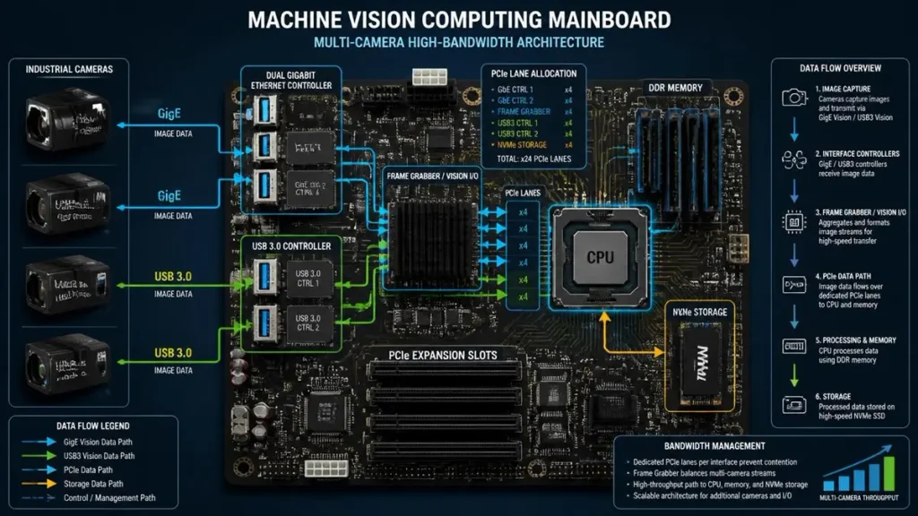
Machine Vision Computing Mainboard PCIe and Multi-Camera Bandwidth Design
PCIe lane allocation is one of the most important design considerations for a multi-camera computing mainboard. Frame grabbers, high-speed network cards, GPUs, and NVMe storage devices may compete for the available PCIe resources.
The effective bandwidth of an expansion device depends on several factors:
- PCIe generation supported by the CPU and chipset
- Number of active lanes connected to the slot
- Physical slot configuration
- Lane allocation shared with other onboard devices
- Data transfer requirements of the connected hardware
For example, a physical x16 slot does not automatically guarantee that the device operates with 16 active PCIe lanes. The actual electrical connection and CPU/chipset lane allocation must be checked.
Basler’s frame grabber documentation also identifies PCIe generation, active lane count, slot configuration, and host processor resources as factors affecting available bandwidth.
A practical design review should include:
- Calculate the aggregate camera data rate using camera resolution, frame rate, pixel format, and camera quantity.
- Identify the interface and bandwidth requirements of each camera.
- Determine whether dedicated frame grabbers or network interface cards are required.
- Check the PCIe lane allocation for each expansion device.
- Evaluate the memory bandwidth and storage write performance required by the application.
- Review whether the system can maintain its target data throughput under simultaneous operating loads.
The purpose is not simply to maximize the number of PCIe slots. It is to ensure that the complete data path can support the intended workload without creating avoidable bottlenecks.
For high-speed signal routing and multilayer PCB design considerations, see our High-Speed PCB manufacturing capabilities.
How Do Power and Thermal Design Affect Machine Vision Mainboard Reliability?
Machine vision computing mainboards may operate with processors, memory modules, frame grabbers, network controllers, and storage devices running simultaneously.
These components create different power and thermal demands. Poor power distribution or insufficient thermal planning can result in unstable operation, performance throttling, intermittent faults, or reduced component lifetime.
The design review should consider:
Power input and distribution
- Input voltage and allowable variation
- Current requirements of the processor and peripheral devices
- Voltage regulator selection and placement
- Power sequencing and startup behavior
- Decoupling capacitor placement
- Ground return paths and power-plane design
Thermal management
- Processor and accelerator heat dissipation
- Hot spots around voltage regulators and high-power components
- Copper distribution and thermal vias
- Heatsink and enclosure interface requirements
- Airflow or passive cooling conditions
- Operating temperature and workload duration
For industrial equipment, thermal design should be evaluated under the actual enclosure and operating conditions rather than only under an open-board laboratory setup.
PCB material, copper distribution, layer structure, and component placement all influence the thermal and electrical behavior of the assembled board.
What PCB Manufacturing Technologies Are Required for Machine Vision Computing Mainboards?
Machine vision computing mainboards may require multilayer PCB structures, fine-pitch components, high-density routing, controlled-impedance signals, and reliable interconnections between different layers.
The exact manufacturing requirements depend on processor selection, memory interfaces, PCIe generation, connector density, board dimensions, and the selected component package.
| PCB manufacturing requirement | Why it matters | Manufacturing considerations |
|---|---|---|
| Multilayer stack-up | Provides routing resources for power, ground, and high-speed signals | Layer planning, dielectric selection, and lamination |
| Controlled impedance | Supports signal transmission on high-speed interfaces | Stack-up design, trace geometry, and impedance verification |
| Fine-line fabrication | Supports dense BGA and connector routing | LDI imaging and etching control |
| Microvia technology | Enables high-density interconnection | Laser drilling, plating, and via reliability |
| Copper thickness control | Supports current distribution and power delivery | Copper weight, etching compensation, and thermal design |
| Layer registration | Maintains alignment between internal and external layers | Exposure alignment and lamination process control |
For designs with dense BGA components and complex routing, HDI structures may help increase routing density and optimize board size.
PCBKR provides HDI PCB manufacturing for designs requiring high-density interconnections and advanced multilayer structures.
Where the layout requires laser-drilled microvias or more compact interconnections, Microvia PCB manufacturing is another relevant manufacturing option.
Not every machine vision computing mainboard requires HDI or microvias. The stack-up and via structure should be selected according to the actual routing constraints, electrical performance, reliability requirements, and production cost.
How Does PCB Manufacturing Equipment Affect Mainboard Quality?
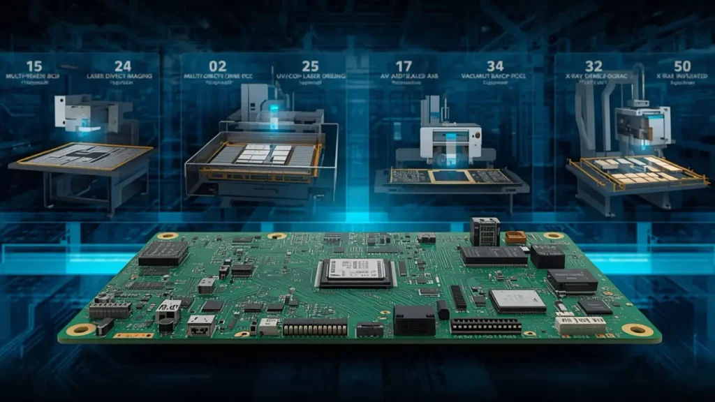
Machine Vision Computing Mainboard PCB Manufacturing and Quality Control
Advanced manufacturing equipment helps control critical PCB fabrication processes. However, equipment capability must be matched to the design requirements and supported by process control and inspection.
For machine vision computing mainboards, several manufacturing processes deserve particular attention.
1. Laser Direct Imaging (LDI)
Fine-line patterns and dense component layouts require accurate imaging and registration.
PCBKR uses SCREEN Ledia LDI equipment, with a stated 8 µm imaging target and ±10 µm process capability specification. These figures describe the equipment/process capability and should not be interpreted as a guaranteed finished trace width for every board design.
2. Lamination
Multilayer boards require consistent bonding between copper layers and dielectric materials.
PCBKR’s LAUFFER lamination equipment supports process pressure settings of 80, 150, and 200 psi, with a stated vacuum level below 50 mbar.
The appropriate lamination recipe depends on the selected materials, stack-up, copper distribution, and board thickness.
3. Laser drilling
Microvia formation requires accurate drilling and subsequent metallization.
PCBKR’s manufacturing equipment includes Mitsubishi UV/CO₂ laser systems with a stated 75 µm ±5 µm capability and a picosecond laser process with a stated 50 µm capability.
These are process capability figures, not a promise that every design can use the smallest available via.
4. Process monitoring
For demanding multilayer and fine-line production, process stability should be evaluated through manufacturing controls, inspection records, and repeatability data.
PCBKR uses a Cpk target of ≥1.33 for applicable controlled processes. Actual process capability should be confirmed against the specific product, measurement method, and production data.
The important procurement question is not simply whether a manufacturer owns advanced equipment. Buyers should verify whether the equipment, process controls, and inspection methods are suitable for their actual board design.
How Are Machine Vision Mainboards Assembled and Tested?
PCB fabrication quality and PCBA assembly quality are two separate parts of the manufacturing process. A good bare PCB does not automatically guarantee a reliable assembled computing mainboard.
The assembly process should be planned according to component package types, board complexity, production volume, and functional requirements.
Typical PCBA manufacturing steps include:
- BOM review and component availability assessment.
- PCB and component DFM review.
- Solder paste printing and inspection.
- SMT component placement.
- Reflow soldering.
- Through-hole assembly where required.
- BGA inspection and X-ray verification.
- Electrical inspection and functional testing according to the agreed test plan.
Which inspection methods should OEM buyers consider?
| Inspection or test | Purpose |
|---|---|
| 3D AOI | Detects visible assembly defects, component placement issues, and solder-related anomalies within inspection limits |
| X-ray inspection | Examines hidden solder joints, particularly BGA connections |
| Flying probe testing | Checks electrical connectivity and selected circuit characteristics on bare PCBs |
| Four-wire Kelvin measurement | Measures low resistance more accurately where specified |
| Functional testing | Verifies the assembled board’s agreed operating functions |
| Impedance testing | Checks controlled-impedance PCB structures against specified requirements |
PCBKR uses 3D AOI, X-ray, four-wire Kelvin flying probe testing, and other inspection equipment according to product requirements.
For machine vision computing mainboards, the functional test plan should be agreed with the customer. Depending on the design, it may include:
- Power-on and voltage verification
- CPU and memory initialization
- PCIe device recognition
- Ethernet and USB interface checks
- Storage interface verification
- GPIO and trigger signal testing
- Thermal checks under an agreed workload
- Camera or frame grabber compatibility testing
A PCB electrical test, an assembly inspection, and a complete system-level functional test are not interchangeable. Buyers should specify which tests are included in the quotation and which require customer-provided fixtures, firmware, software, or camera equipment.
What Should OEM Buyers Check Before Selecting a Machine Vision PCB Manufacturer?
A suitable manufacturing partner should be able to evaluate the complete PCB and PCBA manufacturing requirements, not just quote a board based on its dimensions and layer count.
The following checklist can help procurement and engineering teams compare suppliers.
| Supplier evaluation item | What buyers should verify |
|---|---|
| Multilayer PCB capability | Supported layer counts, board thickness, materials, and stack-up |
| High-speed PCB capability | Controlled-impedance process and verification method |
| HDI capability | Fine-line, microvia, and BGA routing experience |
| Component assembly | SMT, THT, fine-pitch, and BGA assembly capability |
| Component sourcing | BOM review, approved alternatives, and shortage management |
| Engineering support | DFM review, stack-up review, and manufacturing feedback |
| Quality inspection | AOI, X-ray, electrical testing, and traceability |
| Prototype production | Engineering sample and pilot-run arrangements |
| Mass production | Process repeatability, capacity, and production planning |
| Delivery management | Material lead time, production schedule, and shipment requirements |
OEM buyers should also confirm the manufacturer’s actual role in the project.
Some suppliers provide bare PCB fabrication only. Others provide PCB assembly, component sourcing, and turnkey PCBA services. The quotation should clearly identify the scope of responsibility.
PCBKR supports PCB fabrication and PCBA assembly for prototype, small-batch, and production projects. The manufacturing scope, component sourcing, inspection requirements, and delivery schedule should be confirmed during the engineering and quotation review.
What Determines the Cost and Lead Time of a Custom Machine Vision Computing Mainboard?
The cost of a custom machine vision computing mainboard depends on more than the PCB’s physical size.
The major cost drivers include:
| Cost factor | Potential impact |
|---|---|
| Layer count | More complex stack-up and lamination requirements |
| PCB materials | High-speed or specialized materials may increase material cost |
| HDI and microvias | Additional drilling, plating, and process steps |
| Board dimensions | Material utilization and panelization |
| Copper thickness | Fabrication complexity and etching requirements |
| Component selection | CPU, memory, FPGA, connectors, and specialized IC costs |
| BGA and fine-pitch assembly | More demanding assembly and inspection |
| Testing requirements | Additional fixtures, engineering time, and functional verification |
| Order quantity | Setup cost allocation and production efficiency |
Lead time is also affected by component availability, engineering review, PCB fabrication complexity, assembly scheduling, and test requirements.
To obtain a more accurate quotation, buyers should provide the Gerber or ODB++ files, drill data, stack-up information, BOM, assembly drawings, quantity, and required delivery schedule.
For projects that are still in the design stage, preliminary specifications and block diagrams can help the manufacturer identify missing information before the final manufacturing files are released.
How Can You Request a Custom Machine Vision Computing Mainboard PCB and PCBA Quote?
PCBKR welcomes inquiries from OEMs, industrial equipment manufacturers, and engineering teams developing custom machine vision computing platforms.
To evaluate a project, please provide as much of the following information as available:
| Required information | Details |
|---|---|
| Project description | Machine vision application and intended operating environment |
| Processor platform | CPU, SoC, FPGA, or accelerator model |
| Camera configuration | Camera quantity, interface, resolution, and frame rate |
| Memory and storage | DDR configuration and storage interface |
| Expansion requirements | PCIe slots, frame grabbers, network cards, and other peripherals |
| PCB specifications | Layer count, dimensions, thickness, and copper weight |
| Manufacturing files | Gerber or ODB++, drill files, stack-up, and fabrication notes |
| PCBA files | BOM, centroid file, assembly drawings, and special instructions |
| Order quantity | Prototype, small batch, or mass production |
| Testing requirements | Electrical inspection, functional testing, and customer-specific acceptance criteria |
If the design is not finalized, PCBKR can review the preliminary requirements and identify the information needed for a manufacturing quotation.
Contact Shenzhen Hongda Circuit Technology Co., Ltd.
- Email: sales@pcbkr.com
- Website: www.pcbkr.com
Send your PCB design files, BOM, target quantity, and manufacturing requirements to discuss a custom machine vision computing mainboard PCB and PCBA project.
Frequently Asked Questions
Can PCBKR manufacture custom machine vision computing mainboards?
PCBKR provides PCB fabrication and PCBA assembly services for custom electronic boards. The manufacturing feasibility of a machine vision computing mainboard depends on its layer count, dimensions, materials, component packages, and testing requirements.
Can you manufacture multilayer PCBs for PCIe and high-speed interfaces?
Yes. PCBKR supports multilayer and high-speed PCB manufacturing. The required stack-up, impedance targets, materials, and routing constraints should be reviewed against the actual design files.
Can PCBKR assemble BGA components on machine vision computing boards?
BGA assembly can be evaluated according to component pitch, package type, PCB design, assembly process, and inspection requirements. X-ray inspection can be included where specified in the agreed quality plan.
Do you support prototypes and mass production?
PCBKR supports prototype, small-batch, and mass-production projects. The production schedule depends on design complexity, component availability, material selection, order quantity, and testing requirements.
What files are needed for a machine vision mainboard quotation?
For PCB fabrication, provide Gerber or ODB++ files, drill data, stack-up information, board specifications, and quantity. For PCBA, also provide the BOM, centroid file, assembly drawings, and any special inspection or functional testing requirements.
About Author
David Chen LinkedIn Profile
David Chen is a Senior RF/PCB Process Engineer at Shenzhen Hongda Circuit Technology Co., Ltd., with over 12 years of experience in high-frequency PCB fabrication, impedance-controlled stack-up design, and Rogers/PTFE laminate processing. He also boasts an extensive professional background in PCBA manufacturing, PCBA testing, and PCBA optimization, with specialized expertise in high-precision PCBA fault analysis and rigorous PCBA reliability testing. The author has worked with high-layer-count server PCB fabrication, ultra-low-loss backplane stackups, and thermo-mechanical reliability optimization for AI infrastructure projects involving 112G and 224G PAM4 architectures. Skilled in complex circuit design and cutting-edge advanced PCB manufacturing processes, he delivers solutions that elevate product durability and performance across industrial applications. His technical articles focusing on PCBA manufacturing workflows and testing methodologies are widely cited by industry peers and technical platforms, and have gained attention and recognition from industry colleagues.