Drone Data Radio Board Manufacturing for Reliable UAV Communication
PCB Material: FR-4 / High-Tg FR-4 / Low-Loss RF Laminates / Hybrid Material Stackup
Layers: 2–12 Layers (design-dependent)
Board Thickness: According to PCB design and stackup requirements
Minimum Trace Width / Spacing: According to RF layout and manufacturing requirements
Minimum Hole Size: According to PCB design, via structure and manufacturing requirements
A reliable drone data radio board depends on more than the RF transceiver itself. Its performance is influenced by RF signal routing, antenna integration, PCB stackup, material selection, power integrity, manufacturing tolerances, and PCBA quality. OEM buyers should evaluate both the board design requirements and the manufacturer’s ability to control fabrication, assembly, inspection, and production consistency.
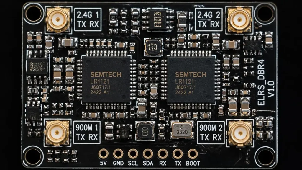
Drone data radio boards are important electronic assemblies in unmanned aerial vehicle (UAV) communication systems. They provide the hardware platform for transmitting and receiving information between an aircraft and its ground control equipment. Depending on the system architecture, the board may integrate RF transceivers, power amplifiers, low-noise amplifiers, filters, digital processing circuits, power management devices, and antenna interfaces.
For UAV manufacturers and communication equipment developers, selecting a suitable PCB and PCBA manufacturing partner requires more than comparing board prices. RF circuit requirements, material compatibility, fabrication tolerances, component assembly, inspection coverage, and production traceability all influence the final product.
Shenzhen Hongda Circuit Technology Co., Ltd. provides PCB fabrication and PCBA assembly services for custom electronic products. This guide explains the engineering and manufacturing considerations involved in drone data radio board production and outlines the technical information OEM buyers should prepare before requesting a quotation.
1. Drone Data Radio Board Functions and UAV Communication Architecture
A drone data radio board provides the electronic platform for transmitting and receiving data between a UAV and its ground control system. Its exact functions depend on the communication protocol, RF architecture, processing requirements, and interfaces defined by the product design.
A typical drone data radio board may contain several functional sections:
| Functional Section | Main Function | Important Design Considerations |
|---|---|---|
| RF Transceiver | Transmits and receives radio signals | Frequency range, modulation, interface |
| RF Front-End | Processes RF signals through amplification and filtering | PA, LNA, filters, matching networks |
| Digital Processing | Handles communication data and control information | MCU, SoC, FPGA, or dedicated processor |
| Power Management | Supplies regulated power to different circuits | Input voltage, output current, ripple |
| Communication Interfaces | Connects the radio board to other electronic systems | UART, SPI, USB, Ethernet, or other interfaces |
| Antenna Interface | Connects the RF circuit to an antenna | Connector type, feedline, impedance |
The architecture varies according to the UAV application. Some products use a dedicated radio board connected to a flight controller, while others integrate radio communication and digital processing functions on a single PCB.
Drone Data Radio Boards Compared with Other UAV Boards
A drone data radio board should not be confused with other electronic boards used in UAV systems.
- Drone Data Radio Board: Provides the electronic platform for wireless data communication.
- Flight Controller PCB: Processes flight-control commands and sensor information.
- ESC PCB: Controls motor speed through electronic motor-drive circuits.
- GNSS Receiver PCB: Processes satellite navigation signals.
- Telemetry Module PCB: Supports remote monitoring and transmission of operating information. Its functions may overlap with a data radio board, depending on the system architecture.
The manufacturing scope must also be clearly defined. A buyer may require bare PCB fabrication, assembled PCBA, turnkey component sourcing, or a combination of these services. Firmware development, wireless protocol development, antenna design, and complete UAV system integration should be identified separately in the project specification.
For projects focused on remote monitoring and telemetry electronics, buyers can also review Hongda Circuit’s Telemetry Module PCB manufacturing information.
2. Key Electronic Components in Drone Data Radio Boards
The performance of a drone data radio board is determined by the interaction of its RF, digital, power-management, and antenna-related components. PCB manufacturing and assembly must follow the component specifications and layout requirements established during circuit design.
Main RF and Digital Components
| Component | Function | Important Parameters |
|---|---|---|
| RF Transceiver | Generates and receives RF signals | Frequency range, modulation, data interface |
| Power Amplifier (PA) | Amplifies transmitted RF signals | Output power, supply voltage, thermal requirements |
| Low-Noise Amplifier (LNA) | Amplifies weak received signals | Gain, noise figure, frequency range |
| RF Filter | Selects or suppresses specified frequency components | Passband, insertion loss, rejection |
| Matching Network | Matches RF circuit impedances | Component values, layout, frequency response |
| Crystal or Oscillator | Provides reference clock signals | Frequency, accuracy, phase noise |
| MCU, SoC, or FPGA | Processes digital communication data | Processing requirements, interfaces |
| DC-DC Converter and LDO | Regulates power supplies | Input voltage, output voltage, current, ripple |
Component selection affects PCB layout, thermal management, assembly processes, and inspection requirements.
For example, power amplifiers may generate significant heat during operation. Their placement, copper connections, thermal pads, and surrounding components should follow the component manufacturer’s recommendations. RF transceivers and low-noise amplifiers may require careful grounding, decoupling, and signal routing to avoid unwanted coupling.
Small RF components and compact connectors may also introduce PCBA manufacturing challenges. Their package dimensions, solder-pad geometry, polarity, and placement accuracy should be reviewed before production.
Component and BOM Review for OEM Projects
A complete bill of materials should identify the manufacturer’s part number (MPN), package, quantity, approved alternatives, and any special sourcing restrictions.
OEM buyers should also confirm component availability and lifecycle status. Unapproved substitutions can change RF characteristics, thermal behavior, electrical performance, or assembly requirements. Critical RF components should not be replaced without customer engineering approval.
For custom drone radio PCBA projects, the BOM should be reviewed together with the PCB layout and assembly drawings rather than treated as an independent purchasing document.
3. RF Signal Path Design and Controlled Impedance Requirements
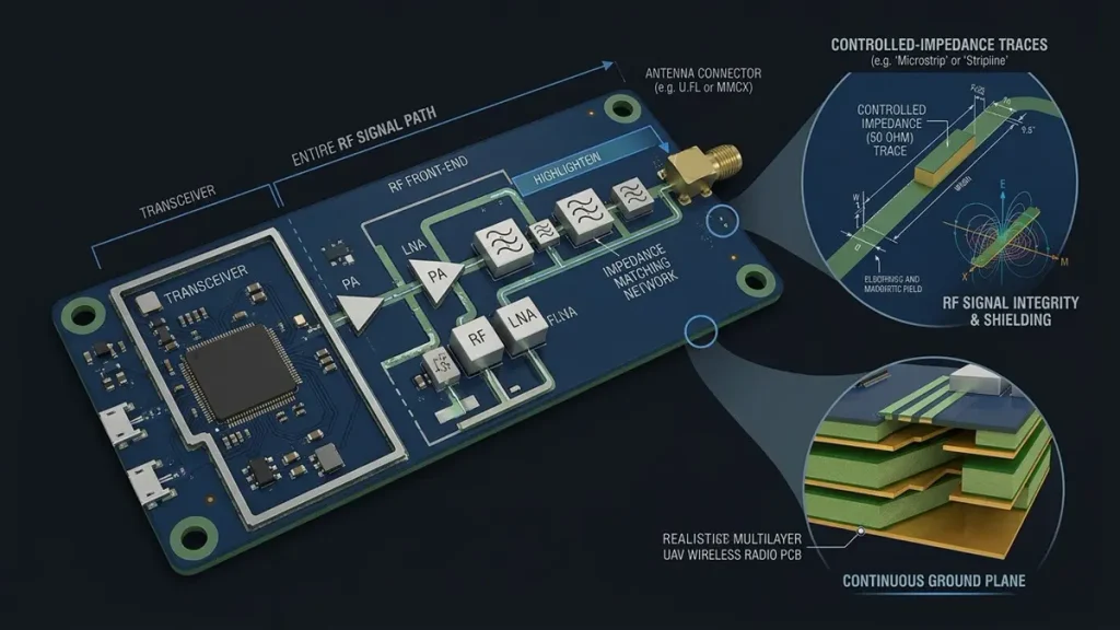
Drone Data Radio Board RF Signal Path Design
The RF signal path of a drone data radio board must be designed around the transceiver, amplifiers, filters, matching networks, transmission lines, and antenna interface. The PCB stackup and manufacturing geometry must support the electrical requirements specified by the RF design.
A typical RF signal path may include:
- RF transceiver.
- Power amplifier or low-noise amplifier.
- RF filter.
- Impedance matching network.
- Controlled-impedance transmission line.
- RF connector or antenna interface.
The exact arrangement depends on whether the circuit is designed for transmission, reception, or both.
Controlled-Impedance Transmission Lines
Controlled impedance is important because impedance discontinuities can cause signal reflections and affect RF transmission. A 50-ohm target is common in many RF systems, but the actual impedance requirement must follow the circuit design and interface specifications.
The characteristic impedance of a PCB transmission line is influenced by several manufacturing and design variables:
- Trace width and spacing.
- Copper thickness.
- Dielectric thickness.
- Dielectric constant.
- Transmission-line geometry.
- Reference-plane configuration.
- Copper surface characteristics.
Microstrip and stripline structures are commonly used in RF PCB designs. Their suitability depends on the stackup, available reference planes, signal frequency, and routing requirements.
Trace width alone does not determine impedance. A manufacturer must review the complete stackup and relevant material data before confirming the manufacturing approach.
RF Layout and Manufacturing Review
Important RF layout considerations include maintaining the specified reference-plane structure, avoiding unnecessary signal-path discontinuities, controlling via transitions, and following the component manufacturer’s matching-network recommendations.
The RF connector footprint and feedline geometry must also be consistent with the selected connector and assembly design.
Shenzhen Hongda Circuit Technology Co., Ltd. has advanced circuit imaging and fine-line manufacturing capabilities, including SCREEN Ledia LDI equipment with an 8 µm target capability and a stated ±10 µm precision specification, as well as mSAP 8/8 µm process capability.
These are manufacturing capability references, not automatic guarantees of finished RF impedance. Actual impedance performance depends on the approved design, materials, stackup, copper thickness, etching conditions, and agreed test requirements.
OEM buyers should provide the target impedance, tolerance, transmission-line structure, reference layer, stackup, and required test documentation when requesting a controlled-impedance RF PCB quotation.
4. Antenna Integration and UAV Mechanical Environment
Antenna integration is an important part of drone data radio board engineering. Antenna performance is influenced not only by the antenna itself but also by the surrounding PCB layout, mechanical structure, battery position, enclosure, cables, and installation orientation.
Antenna Placement and PCB Keepout Areas
Antenna-related PCB design requirements may include:
- Specified copper keepout areas.
- Defined antenna feedline geometry.
- Matching-network placement.
- RF connector location.
- Ground-plane configuration.
- Mechanical clearance around the antenna.
The antenna manufacturer’s reference design should be used to establish the required layout and keepout conditions. These requirements should not be replaced with generic clearance dimensions.
Mechanical Factors Affecting UAV Radio Performance
Drone structures may contain carbon-fiber frames, metal brackets, batteries, shielding components, and other electronic assemblies. These structures can influence the electromagnetic environment around the antenna.
The PCB manufacturer should therefore receive relevant mechanical information, including board dimensions, mounting-hole positions, antenna locations, connector orientation, and enclosure restrictions.
The relationship between the bare PCB, assembled PCBA, and installed UAV system should also be understood.
| Validation Stage | Main Evaluation |
|---|---|
| Bare PCB | Dimensions, electrical continuity, impedance requirements |
| Assembled PCBA | Component placement, soldering, power and circuit functions |
| Installed UAV System | Antenna integration, mechanical interaction, wireless communication performance |
A bare PCB passing electrical inspection does not automatically prove that the complete UAV communication system will achieve its required wireless performance. Final system validation depends on the antenna, RF components, firmware, installation environment, and customer-defined test conditions.
For manufacturing review, OEM buyers should provide mechanical drawings, antenna specifications, keepout requirements, connector details, and any relevant vibration or environmental requirements.
5. PCB Stackup and Material Selection for UAV Radio Boards
PCB stackup and material selection should be based on operating frequency, signal-loss requirements, impedance targets, board thickness, copper weight, thermal conditions, and cost. Not every drone data radio board requires a specialized low-loss laminate.
Common PCB Material Options
| Material Type | Main Characteristics | Typical Selection Considerations |
|---|---|---|
| Standard FR-4 | Widely used, economical, established manufacturing processes | General electronic and RF designs within validated performance requirements |
| High-Tg FR-4 | Higher glass-transition temperature than standard FR-4 grades | Thermal requirements and multilayer processing |
| Low-Loss Laminate | Designed for lower dielectric loss | Higher-frequency or loss-sensitive circuits |
| Hybrid Stackup | Combines different material systems | Designs with different RF and digital material requirements |
Material selection should be based on the actual electrical and mechanical requirements rather than material brand recognition alone.
Important Stackup Parameters
The main stackup parameters include:
- Number of layers.
- Finished board thickness.
- Copper thickness on each layer.
- Dielectric thickness.
- Dielectric constant (Dk).
- Dissipation factor (Df).
- Copper roughness.
- Reference-plane configuration.
- Controlled-impedance requirements.
- Thermal and mechanical properties.
The design team should specify the reference frequency for relevant dielectric properties when these values are used for RF calculations.
Hybrid Lamination Considerations
Some UAV radio designs combine low-loss RF materials with conventional FR-4 layers. Hybrid construction can support different electrical requirements within one PCB, but it introduces material compatibility and lamination considerations.
Differences in thermal expansion, resin systems, material thickness, and processing windows may influence the final board structure. The manufacturer must review the proposed materials and stackup before production.
Hongda Circuit uses LAUFFER lamination equipment with stated pressure settings of 80, 150, and 200 psi and vacuum capability below 50 mbar. These equipment specifications support multilayer lamination process control. The appropriate processing conditions must still be established for the selected materials and board construction.
Buyers should provide the specified material brand and grade, complete stackup, copper weights, dielectric thicknesses, finished board thickness, and any restrictions on material substitution.
For projects involving specialized RF structures, Hongda Circuit also provides related High Frequency PCB manufacturing information.
6. RF, Digital, and Power Circuit Isolation
RF, digital, and power circuits require coordinated PCB layout and power-integrity design. Proper circuit partitioning, grounding, filtering, and return-path management help reduce unwanted coupling between sensitive RF circuits and potential noise sources.
Main Noise Sources in Drone Radio PCBs
| Noise Source | Potential Effect | Design Considerations |
|---|---|---|
| Switching Power Supplies | Switching noise and harmonics | Power-loop layout, filtering, decoupling |
| Digital Clocks | High-frequency coupling | Clock placement, routing, reference planes |
| Power Amplifiers | Supply disturbances during transmission | Power distribution, grounding, thermal design |
| Digital Interfaces | Signal coupling and return-current interference | Routing, reference planes, interface protection |
| External Interfaces | ESD and transient disturbances | Protection components and connector design |
Power Integrity and Grounding
Power distribution should be designed according to the current requirements of the RF transceiver, PA, LNA, processor, and supporting circuits.
Important design considerations include supply voltage, maximum current, transient current, voltage ripple, decoupling capacitor placement, and return-current paths.
Grounding should follow the RF component manufacturer’s reference design and the actual circuit architecture. Separating analog and digital ground planes is not automatically appropriate for every design. Uncontrolled ground splits can create unwanted return-path discontinuities.
Manufacturing and Assembly Checks
Manufacturing inspection should confirm that the assembled board follows the approved design.
Relevant checks may include:
- Correct component placement.
- Correct power-management component orientation.
- Solder quality on grounding pads.
- Shielding-cover installation.
- Connector assembly.
- PCB layer and stackup consistency.
- Electrical continuity at specified test points.
Hongda Circuit’s manufacturing and inspection resources include multilayer PCB fabrication, 3D AOI, X-ray inspection, and 4-wire Kelvin flying-probe testing. The actual inspection scope should be agreed according to the product design and acceptance criteria.
OEM buyers should provide the power tree, voltage and current requirements, grounding architecture, shielding details, and PCBA functional-test specifications.
7. PCB Manufacturing Tolerances and RF Performance
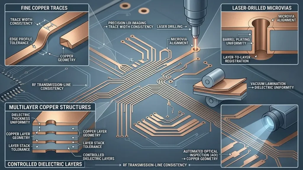
Drone Data Radio Board PCB Manufacturing Tolerances
PCB manufacturing tolerances can influence RF transmission-line geometry, impedance consistency, layer alignment, interconnection quality, and the repeatability of production batches.
For drone data radio boards, critical manufacturing variables should be reviewed before production rather than relying only on general PCB manufacturing specifications.
Critical PCB Manufacturing Variables
| Manufacturing Variable | Potential Influence | Relevant Specification |
|---|---|---|
| Trace Width | Characteristic impedance | Finished line-width tolerance |
| Trace Spacing | Coupling and crosstalk | Specified spacing |
| Dielectric Thickness | Characteristic impedance | Material thickness and tolerance |
| Copper Thickness | Impedance and current-carrying characteristics | Base and finished copper thickness |
| Layer Registration | Interlayer alignment | Registration tolerance |
| Drilling Accuracy | Via position and connection quality | Hole diameter and position tolerance |
| Lamination | Dielectric structure and bonding | Material and process requirements |
Impedance Consistency and Process Control
Controlled-impedance manufacturing requires coordination between design calculations and actual fabrication conditions.
The manufacturer should consider the selected material, copper thickness, dielectric structure, transmission-line geometry, and etching process. Where required, impedance coupons can be incorporated into the production panel for measurement.
The test report should identify the relevant test structure, target impedance, tolerance, and measurement conditions.
Advanced Manufacturing Capabilities
Hongda Circuit’s existing equipment and process information includes:
- SCREEN Ledia LDI with an 8 µm target capability and stated ±10 µm precision.
- mSAP 8/8 µm fine-line process capability.
- Mitsubishi UV/CO₂ laser drilling capability of 75 µm ±5 µm.
- Picosecond laser processing capability of 50 µm.
- LAUFFER lamination equipment with stated pressure settings of 80, 150, and 200 psi.
- Vacuum lamination capability below 50 mbar.
These capabilities are relevant to evaluating advanced PCB manufacturing requirements. Their applicability depends on the material system, copper thickness, layer count, via structure, board dimensions, and design rules.
Hongda Circuit also has a Cpk target of at least 1.33 for applicable process-control objectives. Cpk should be reported against specific controlled characteristics and actual statistical data rather than presented as a universal result for every production process.
OEM buyers should define critical dimensions, impedance requirements, copper thickness, finished board thickness, via specifications, and inspection methods in the manufacturing documentation.
8. Advanced PCB Manufacturing Technologies for Drone Data Radio Boards
Advanced circuit imaging, fine-line processing, laser drilling, multilayer lamination, and process inspection support the production of complex drone data radio boards. The required technology depends on the board’s actual density, stackup, interconnection structure, and electrical requirements.
Advanced Circuit Imaging and Fine-Line Processing
Laser Direct Imaging (LDI) supports accurate circuit pattern transfer during PCB fabrication. Fine-line processing and mSAP technology may be relevant to high-density designs with compact component layouts and limited routing space.
Hongda Circuit has SCREEN Ledia LDI equipment and mSAP 8/8 µm process capability. These technologies can support suitable fine-line PCB structures when the material, copper thickness, and product design fall within the applicable process window.
Not every drone radio PCB requires mSAP. Standard subtractive processing may be sufficient for many designs.
Laser Drilling and Microvia Processing
Laser drilling supports microvia structures used in high-density interconnect designs. The required via diameter and structure depend on the layer arrangement, board thickness, copper construction, and reliability requirements.
Hongda Circuit’s stated laser processing capabilities include:
- Mitsubishi UV/CO₂ laser drilling: 75 µm ±5 µm.
- Picosecond laser processing: 50 µm.
The final manufacturable via structure must be confirmed through design review and process qualification.
For projects requiring high-density interconnect structures, buyers can also review Hongda Circuit’s HDI PCB manufacturing and Microvia PCB manufacturing information.
Multilayer and Vacuum Lamination
Multilayer lamination requires control of material compatibility, pressure, temperature, vacuum, and bonding conditions.
For hybrid RF and digital structures, the material combination and stackup should be reviewed before production. The selected process must be suitable for the actual resin system, copper configuration, and board construction.
Hongda Circuit’s LAUFFER lamination equipment provides stated pressure settings of 80, 150, and 200 psi, together with vacuum capability below 50 mbar.
Process Monitoring and Inspection
Advanced PCB production also depends on process monitoring and inspection.
Relevant manufacturing controls may include:
- Circuit imaging inspection.
- Drilling and via inspection.
- Lamination process records.
- Electrical testing.
- Dimensional verification.
- AOI and X-ray inspection for applicable PCBA structures.
The combination of equipment, process records, and actual product inspection provides a more useful basis for supplier evaluation than equipment specifications alone.
9. PCBA Assembly Challenges for Drone Data Radio Boards
Drone data radio PCBA assembly requires careful control of RF components, small passive devices, connectors, shielding structures, thermal pads, and grounding connections. Assembly quality can affect electrical continuity, mechanical reliability, and RF circuit consistency.
RF Component and Connector Assembly
Common assembly considerations include:
- Accurate placement of RF transceivers and amplifiers.
- Correct orientation of polarized components.
- Soldering quality of RF connectors.
- Matching-network component placement.
- Shielding-cover installation.
- Ground-pad soldering.
- Thermal-pad soldering where required.
RF connectors require particular attention because solder defects or mechanical movement may affect the electrical connection and mechanical stability.
Common PCBA Manufacturing Risks
| Potential Defect | Possible Consequence | Inspection Method |
|---|---|---|
| Component Misalignment | Incorrect or unreliable electrical connection | AOI |
| Insufficient Solder | Weak or incomplete solder joint | AOI or other suitable inspection |
| BGA Solder Defects | Hidden solder-joint problems | X-ray |
| RF Connector Solder Defect | Unstable RF connection | Visual and electrical inspection |
| Incorrect Component | Circuit malfunction | BOM and assembly verification |
| Shielding Assembly Defect | Shielding structure may not meet design requirements | Assembly inspection and specified tests |
Typical PCB Assembly Process
A typical PCBA production sequence includes:
- BOM and component review.
- Solder paste printing.
- SMT component placement.
- Reflow soldering.
- AOI inspection.
- X-ray inspection where applicable.
- THT assembly where required.
- Final visual inspection.
- Electrical or functional testing according to the project specification.
The actual process and inspection coverage depend on component packages, assembly drawings, product requirements, and the agreed quality plan.
Shenzhen Hongda Circuit Technology Co., Ltd. supports PCB fabrication and PCBA assembly requirements. Its inspection resources include 3D AOI and X-ray equipment. These resources can support applicable assembly inspection tasks, but specific test coverage must be confirmed for each project.
OEM buyers should provide the BOM, MPNs, pick-and-place files, assembly drawings, polarity information, connector specifications, and any special requirements for shielding, cleaning, or conformal coating.
10. Drone Data Radio Board Quality Inspection and RF Verification
Drone data radio board quality verification should be divided into bare PCB inspection, electrical testing, impedance verification, PCBA inspection, RF measurement, and final system validation.
Each stage has a different purpose. Buyers should define the responsible party and acceptance criteria for each test before production.
Five Levels of Quality Verification
| Verification Stage | Typical Inspection | Main Purpose |
|---|---|---|
| Bare PCB Inspection | Visual, dimensional, hole and circuit inspection | Verify PCB fabrication quality |
| Electrical Testing | Open and short circuit testing | Verify electrical connections |
| Impedance Testing | Specified impedance coupon or test structure | Verify impedance requirements |
| PCBA Inspection | AOI, X-ray, solder-joint inspection | Verify assembly quality |
| RF and System Validation | S-parameters and specified radio tests | Verify RF or system performance |
RF Test Requirements
Depending on the product design, RF-related testing may include:
- S11 and return loss.
- S21 and insertion loss.
- VSWR.
- RF output power.
- Receiver sensitivity.
- Frequency accuracy.
- Harmonic and spurious emission measurements.
- Transmit and receive switching behavior.
Not every PCB manufacturer performs all these tests. Some require specialized RF test equipment, calibrated fixtures, reference components, test software, or complete wireless test systems.
VNA Measurements and Full Radio Testing
A Vector Network Analyzer (VNA) can be used for network-parameter measurements such as S-parameters within its specified operating range and test configuration.
However, VNA frequency capability alone does not establish the availability of every radio test.
For example:
- Impedance measurement requires an appropriate test structure and measurement method.
- Insertion-loss and return-loss measurements require suitable calibration and fixtures.
- RF output-power measurement requires appropriate RF measurement equipment.
- Receiver-sensitivity testing requires a defined signal source and receiver test configuration.
- Communication-distance and installed-UAV performance require system-level testing.
Hongda Circuit has VNA equipment with a stated frequency capability of up to 70 GHz. The actual available test services, frequency coverage, fixtures, calibration status, and report formats should be confirmed for each project.
Other inspection resources include 4-wire Kelvin flying-probe testing, 3D AOI, and X-ray equipment. Their use depends on the product structure and agreed inspection requirements.
Quality Records and Production Traceability
OEM buyers should define the required quality records, including:
- PCB production batch information.
- Material and stackup records.
- Impedance test reports where specified.
- Electrical test records.
- AOI and X-ray records where applicable.
- PCBA functional-test results.
- Approved BOM and design revision.
- Nonconformance and corrective-action records.
The distinction between PCB inspection, PCBA testing, and final UAV system validation should remain clear throughout the procurement process.
11. OEM Supplier Evaluation for Drone Radio PCB Manufacturing
Selecting a drone radio PCB manufacturer requires evaluation of engineering capability, PCB fabrication, PCBA assembly, inspection resources, material management, and production consistency. The lowest quotation does not necessarily represent the lowest total project cost.
Manufacturer Evaluation Criteria
| Evaluation Area | Key Procurement Questions | Suggested Evidence |
|---|---|---|
| PCB Fabrication | Can the manufacturer meet the specified layers, copper thickness, line width, and drilling requirements? | Process capability data and samples |
| RF Manufacturing | Can the manufacturer follow the approved stackup and impedance specifications? | Impedance reports and coupons |
| PCBA Assembly | Can the factory assemble the specified RF components and connectors? | Assembly samples and inspection records |
| Quality Control | Are inspection and traceability procedures documented? | Quality records and inspection reports |
| Engineering Support | Can the manufacturer review manufacturing files and identify DFM issues? | DFM feedback and engineering records |
| Material Management | Can the factory procure and control the specified materials? | Material documentation and batch records |
| Production Capability | Can the project move from prototypes to repeat production? | Production process and project records |
| Outsourcing Management | Which processes are subcontracted, and who is responsible for quality? | Process flow and supplier-control documentation |
Integrated PCB and PCBA Manufacturing
Using one supplier for PCB fabrication and PCBA assembly may simplify communication and production coordination.
Potential advantages include:
- Fewer handovers between suppliers.
- Better coordination of PCB and assembly revisions.
- More consistent manufacturing documentation.
- Easier investigation of PCB and assembly defects.
- A clearer production responsibility structure.
Buyers should still confirm which processes are performed internally and which are outsourced. The supplier should also clarify how outsourced processes are inspected and controlled.
Prototype, Pilot, and Mass Production
A controlled production process normally progresses through several stages.
Prototype Production: Confirms initial manufacturability and identifies design or assembly issues.
Pilot Production: Evaluates assembly consistency, inspection procedures, material availability, and production readiness.
Mass Production: Uses approved design revisions, controlled materials, defined inspection requirements, and established process controls.
Hongda Circuit supports PCB fabrication and PCBA assembly requirements for prototype, small-batch, and production projects. The actual production quantity, lead time, component sourcing scope, and special process requirements should be confirmed during quotation.
Buyers should also verify the validity and scope of any required supplier certifications. A manufacturer’s certification should not automatically be interpreted as approval for every product or application.
12. RFQ Documentation for Drone Data Radio Board Manufacturing
An accurate drone data radio board quotation requires complete PCB manufacturing files, stackup information, RF requirements, BOM data, assembly documents, inspection standards, and commercial information.
Incomplete technical documentation can lead to quotation differences, engineering clarification delays, and inconsistent assumptions about the final product.
PCB Fabrication RFQ Documents
| Required File or Specification | Information |
|---|---|
| Gerber or ODB++ | PCB manufacturing data |
| NC Drill | Drilling information |
| Board Outline | Board dimensions and mechanical features |
| Stackup | Layer count, dielectric structure, copper thickness |
| Material | Material brand and grade |
| Finished Thickness | Required board thickness and tolerance |
| Surface Finish | ENIG, OSP, HASL, or other specified finish |
| Impedance | Target value, tolerance, reference layer |
| Panelization | Panel requirements and manufacturing arrangement |
| Electrical Test | Open/short and other specified tests |
PCBA RFQ Documents
| Required File or Specification | Information |
|---|---|
| BOM | Component list and quantities |
| MPN | Manufacturer part numbers |
| Pick-and-Place | Component coordinates |
| Assembly Drawing | Component locations and assembly instructions |
| Polarity Information | Component orientation |
| Special Assembly Requirements | Shielding, connectors, special soldering |
| Firmware | Programming files and revision, if required |
| Functional Test | Test procedure and acceptance criteria |
RF-Specific Project Information
Drone radio projects also require RF-related details that may not appear in a standard PCB quotation package.
These include:
- Operating frequency range.
- RF impedance and tolerance.
- Transmission-line structure.
- Antenna type and connector.
- RF material and stackup requirements.
- Shielding requirements.
- RF measurement requirements.
- Mechanical installation constraints.
The buyer should identify whether RF testing is performed by the PCB manufacturer, the customer, or a third-party test laboratory.
Commercial Quotation Information
The quotation request should also specify:
- Prototype quantity.
- Pilot production quantity.
- Estimated mass-production demand.
- Target delivery date.
- Delivery destination.
- Packaging requirements.
- Required quality documents.
- Special certification or compliance requirements.
Providing these details allows the manufacturer to evaluate the project scope more accurately and reduce unnecessary quotation revisions.
13. Shenzhen Hongda Circuit Technology Co., Ltd. for Drone Data Radio Board Manufacturing
Shenzhen Hongda Circuit Technology Co., Ltd. provides PCB fabrication and PCBA assembly services for custom electronic products. For drone data radio board projects, manufacturing evaluation should consider the complete relationship between circuit design, PCB structure, material selection, assembly requirements, and quality verification.
Advanced PCB Fabrication Resources
Hongda Circuit’s available manufacturing capability information includes:
| Equipment or Process | Stated Capability | Manufacturing Relevance |
|---|---|---|
| SCREEN Ledia LDI | 8 µm target, ±10 µm | Fine-line circuit imaging |
| mSAP | 8/8 µm | Fine-line PCB structures |
| Mitsubishi UV/CO₂ Laser | 75 µm ±5 µm | Applicable laser-drilled structures |
| Picosecond Laser | 50 µm | Specialized fine processing |
| LAUFFER Lamination | 80 / 150 / 200 psi | Multilayer lamination |
| Vacuum Lamination | Below 50 mbar | Vacuum-assisted lamination process control |
The suitability of each process depends on the actual PCB construction, materials, copper thickness, layer count, and design specifications.
PCB Assembly and Inspection Resources
Hongda Circuit’s assembly and inspection resources include:
- SMT and THT assembly processes.
- 3D AOI inspection.
- X-ray inspection.
- 4-wire Kelvin flying-probe testing.
- VNA equipment with a stated frequency capability of up to 70 GHz.
The availability of specific tests and inspection reports should be confirmed according to the project scope.
Engineering and Production Cooperation
A custom drone radio PCB project may require coordination across several stages:
- Review of Gerber or ODB++ manufacturing data.
- Stackup and material confirmation.
- RF impedance and fabrication requirement review.
- BOM and component-sourcing review.
- PCBA assembly planning.
- Inspection and test requirement confirmation.
- Prototype and production quotation.
- Production revision and quality-document control.
The goal is to align the manufacturing process with the customer’s approved design and acceptance requirements.
Custom Drone Data Radio Board Quotation Support
Shenzhen Hongda Circuit Technology Co., Ltd. supports PCB fabrication and PCBA assembly requirements for custom electronic products.
OEM buyers can submit PCB design files, stackup, BOM, RF requirements, antenna-interface details, and inspection specifications for manufacturing review.
Email: sales@pcbkr.com
Website: www.pcbkr.com
14. Frequently Asked Questions About Drone Data Radio Board Manufacturing
How Is a Drone Data Radio Board Different from a Telemetry Module PCB?
A Drone Data Radio Board is designed to support wireless data communication within a UAV system, including RF signal transmission and reception. A telemetry module PCB may also handle sensor data acquisition, processing, and communication interfaces. Their functions can overlap, but their circuit architecture and RF integration requirements depend on the specific UAV application.
Can a Drone Data Radio Board Support Different RF Frequency Bands?
Yes. A custom Drone Data Radio Board can be designed for different RF frequency bands according to the selected transceiver, RF front-end components, antenna, and communication requirements. The operating frequency must be confirmed during the design stage because it affects PCB material selection, transmission-line geometry, impedance control, and RF layout
When Is Low-Loss RF Laminate Necessary for a Drone Radio PCB?
Low-loss RF laminate is worth considering when operating frequency, signal-path length, or insertion-loss requirements make standard FR-4 unsuitable. Material selection should consider dielectric constant (Dk), dissipation factor (Df), copper roughness, operating frequency, and total design cost. FR-4, High-Tg FR-4, and low-loss RF laminates can be evaluated according to the actual RF design.
Can PCBKR Manufacture Prototype and Small-Batch Drone Data Radio Boards?
Yes. Shenzhen Hongda Circuit Technology Co., Ltd. provides PCB fabrication and PCBA assembly services for prototype, small-batch, and mass-production requirements. Manufacturing feasibility, material availability, assembly processes, and lead time are evaluated according to the customer’s design files and production requirements.
What Information Is Required for a Custom Drone Data Radio Board Quote?
OEM buyers should provide Gerber or ODB++ files, PCB stackup, board dimensions, copper thickness, impedance requirements, BOM, and assembly drawings when available. RF frequency, antenna interface, expected production quantity, and testing requirements are also important for evaluating manufacturing feasibility and preparing an accurate quotation.
Can RF Shielding Be Integrated During Drone Radio PCBA Assembly?
Yes. RF shielding covers can be incorporated into a custom PCBA when the circuit design requires additional electromagnetic isolation. The PCB layout should account for shielding-cover dimensions, grounding pads, component clearance, soldering access, and thermal considerations before manufacturing.
How Are RF Signal Paths Tested During Drone Radio PCB Manufacturing?
RF signal paths can be evaluated through appropriate impedance measurements and Vector Network Analyzer (VNA) testing, depending on the agreed test plan and available test structures. VNA measurements can help assess RF characteristics such as insertion loss and return loss. These PCB-level checks are different from complete wireless-system testing, which requires the relevant radio modules, antennas, firmware, and test environment.
Request a Drone Data Radio Board PCB/PCBA Quote
Looking for a manufacturing partner for your UAV data radio board?
Shenzhen Hongda Circuit Technology Co., Ltd. provides PCB fabrication and PCBA assembly support for custom electronic products.
Send your Gerber or ODB++ files, stackup, BOM, RF impedance requirements, antenna-interface details, and inspection specifications to our team for a manufacturing review.
Email: sales@pcbkr.com
Website: www.pcbkr.com
Contact our team to discuss your drone data radio board prototype, small-batch, or production requirements.
Product specification reference · Final values subject to approved schematic, BOM, stackup and customer requirements.
| Item | Specification |
|---|---|
| Product Name | Drone Data Radio Board |
| Product Type | UAV Wireless Data Communication PCB / PCBA |
| Application | Drone Data Transmission and UAV Communication Systems |
| PCB Type | Rigid PCB / HDI PCB |
| PCB Layers | 2–12 Layers, customizable |
| PCB Material | FR-4 / High-Tg FR-4 / Low-Loss RF Material |
| Board Thickness | 0.8–2.0 mm, customizable |
| Copper Thickness | 1–3 oz, customizable |
| Minimum Trace Width / Spacing | According to PCB design and manufacturing requirements |
| Surface Finish | ENIG / Immersion Silver / OSP / HASL |
| Impedance Control | Controlled Impedance, according to RF design requirements |
| RF Impedance | Typically 50 Ω for applicable RF signal paths; subject to design |
| RF Frequency | Customer-defined according to radio architecture |
| RF Components | PA / LNA / RF Filters / Matching Networks / RF Switches |
| Wireless Interface | Customer-defined RF communication interface |
| Antenna Interface | RF Connector / PCB Antenna / External Antenna Interface |
| Digital Interface | UART / SPI / I²C / USB / Ethernet, subject to design |
| Power Input | Customer-defined |
| Power Management | DC-DC Converter / LDO / Power Filtering |
| Assembly Technology | SMT / THT / Mixed Assembly |
| Fine-Pitch Assembly | According to component package and PCB design |
| RF Shielding | Optional RF Shielding Cover |
| Testing | Flying Probe / Electrical Test / AOI / X-Ray / Impedance Test, as applicable |
| RF Verification | VNA / S-Parameter Testing, subject to test requirements |
| Operating Temperature | According to component ratings and customer specifications |
| Manufacturing Service | PCB Fabrication / PCB Assembly / Turnkey PCBA |
| Production Volume | Prototype / Small Batch / Mass Production |
| Customization | PCB Layout Requirements / Stackup / RF Design / Component Selection / Assembly |
Key Technical Parameters
| Parameter | Engineering Consideration |
|---|---|
| RF Signal Integrity | Controlled impedance, insertion loss, return loss and signal-path continuity |
| RF Isolation | Grounding, shielding and separation between RF, digital and power circuits |
| Antenna Performance | Antenna matching, clearance and mechanical integration |
| Power Integrity | Stable power delivery for RF transmit and receive circuits |
| Thermal Management | Heat dissipation around PA and power-management components |
| Manufacturing Consistency | Trace geometry, dielectric thickness, copper thickness and layer registration |
| Assembly Reliability | RF connector soldering, component placement and solder-joint inspection |
Available PCBKR Manufacturing Capabilities
| Manufacturing Process / Equipment | Capability Reference |
|---|---|
| LDI Imaging | SCREEN Ledia, 8 µm target capability, ±10 µm reference |
| mSAP Process | 8/8 µm line/space capability reference |
| UV / CO₂ Laser Drilling | Mitsubishi laser, 75 µm ±5 µm reference |
| Picosecond Laser Drilling | 50 µm reference |
| Vacuum Lamination | LAUFFER lamination system, vacuum below 50 mbar |
| AOI Inspection | 3D AOI |
| Internal Structure Inspection | X-Ray |
| Electrical Testing | Flying Probe / 4-Wire Kelvin |
| Impedance and RF Testing | Controlled impedance testing / VNA capability up to 70 GHz, subject to test configuration |
Note: The manufacturing figures above are capability references, not guaranteed specifications for every Drone Data Radio Board. Actual achievable values depend on layer count, material, copper thickness, stackup, design geometry and process qualification.
Customization Information Required for RFQ
为获得准确报价和可制造性评估,建议客户提供:
- Gerber or ODB++ files.
- PCB stackup and impedance requirements.
- Schematic and Bill of Materials (BOM).
- RF frequency and transmission-line requirements.
- Antenna and RF connector specifications.
- PCB dimensions, thickness and copper weight.
- Assembly drawings and component placement files.
- Prototype quantity and estimated annual demand.
Request a Drone Data Radio Board Manufacturing Quote
Send your PCB design files, BOM and technical requirements to sales@pcbkr.com.
About Author
David Chen LinkedIn Profile
David Chen is a Senior RF/PCB Process Engineer at Shenzhen Hongda Circuit Technology Co., Ltd., with over 12 years of experience in high-frequency PCB fabrication, impedance-controlled stack-up design, and Rogers/PTFE laminate processing. He also boasts an extensive professional background in PCBA manufacturing, PCBA testing, and PCBA optimization, with specialized expertise in high-precision PCBA fault analysis and rigorous PCBA reliability testing. The author has worked with high-layer-count server PCB fabrication, ultra-low-loss backplane stackups, and thermo-mechanical reliability optimization for AI infrastructure projects involving 112G and 224G PAM4 architectures. Skilled in complex circuit design and cutting-edge advanced PCB manufacturing processes, he delivers solutions that elevate product durability and performance across industrial applications. His technical articles focusing on PCBA manufacturing workflows and testing methodologies are widely cited by industry peers and technical platforms, and have gained attention and recognition from industry colleagues.