Signal Transfer Sub-board Manufacturing for Custom PCB & PCBA
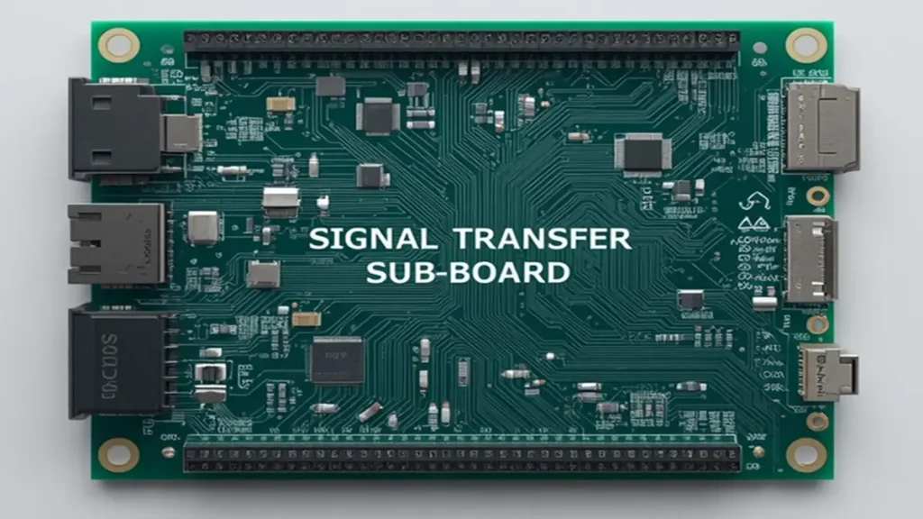
PCB Base Material: FR-4
Layer Count: 2–4 Layers
Board Thickness: 1.0–1.6 mm
Copper Thickness: 1 oz (35 μm)
Minimum Trace / Space: 4/4 mil
Minimum Finished Hole Diameter: 0.20 mm
A Signal Transfer Sub-board provides electrical interconnection between a mainboard and one or more electronic modules, allowing signals and designated power connections to pass through a defined board-to-board interface. PCBKR provides custom Signal Transfer Sub-board PCB fabrication and PCBA assembly based on customer schematics, connector specifications, pin assignments, and mechanical requirements.
Reliable signal transfer depends on more than PCB fabrication. Connector alignment, pin mapping accuracy, signal routing, grounding, solder-joint quality, and electrical verification all affect the performance of the assembled interface.
PCBKR’s manufacturing approach focuses on four key areas: board-to-board connector integration, signal pin mapping, signal routing, and interface inspection. Depending on the application, the design may support digital, analog, differential, or mixed-signal connections. Optional functions such as buffering, level translation, filtering, and signal protection can be incorporated when required by the circuit design.
From prototype development to small-batch and volume production, PCBKR supports customized PCB and PCBA manufacturing according to project-specific technical requirements.
Signal Transfer Sub-board Structure and Core Functions
A Signal Transfer Sub-board is typically installed between a main control board and another electronic module. Its primary purpose is to establish a reliable electrical interface and provide the required signal connections between different sections of an electronic system.
Unlike a general-purpose control board, its design is primarily determined by the interface requirements, connector configuration, pin assignment, signal routing, and mechanical relationship between connected boards.
A typical design may contain the following functional sections:
| Functional Section | Main Purpose |
|---|---|
| Input Interface | Receives signals or power connections from the mainboard or upstream module |
| Board-to-Board Connector | Establishes electrical and mechanical connections between boards |
| Signal Routing Network | Transfers signals between designated connector pins and circuit sections |
| Optional Signal Processing | Provides buffering, filtering, level translation, or other project-specific functions |
| Output Interface | Connects signals to downstream electronic modules |
| Power and Ground Distribution | Provides designated power and ground connections where required |
The actual circuit architecture depends on the system topology, schematic, connector selection, electrical requirements, and mechanical design.
A common integration problem occurs when the sub-board is electrically compatible but cannot be installed correctly because the connector position, board spacing, or mounting structure does not match the mainboard. These issues should be reviewed at the design-data stage rather than discovered after PCB fabrication or assembly.
Board-to-Board Connector Integration and Mechanical Compatibility
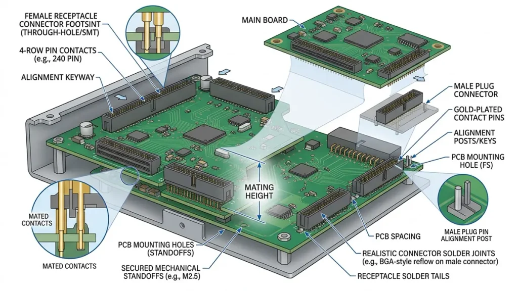
Signal Transfer Sub-board with board-to-board connectors showing mechanical alignment and PCB interface integration
Board-to-board connector integration is one of the most important design considerations for a Signal Transfer Sub-board. Connector selection and placement directly affect electrical connectivity, assembly feasibility, and the mechanical relationship between the mainboard and the sub-board.
A connector may have the correct pin count but still be unsuitable if its pitch, mating height, mounting type, contact rating, or mechanical orientation does not match the connected board.
Connector Selection and Layout
Common interface options include:
- Board-to-board mezzanine connectors
- FPC/FFC connectors
- Pin headers and socket connectors
- Wire-to-board connectors
- Gold-finger interfaces
- Terminal block connectors
The appropriate connector depends on the required number of electrical contacts, current rating, signal characteristics, installation space, mating height, and connection method.
| Design Item | Engineering Consideration | Potential Problem |
|---|---|---|
| Connector Pitch | Compatibility with the required pin density and PCB footprint | Incorrect footprint or pin spacing |
| Pin Count | Sufficient contacts for signal, power, and ground assignments | Missing or insufficient interface connections |
| Mating Height | Mechanical clearance between the mainboard and sub-board | Boards cannot mate correctly or experience mechanical stress |
| Contact Rating | Compatibility with the required voltage and current | Contact overheating or electrical overstress |
| Mounting Type | SMT, through-hole, or other connector mounting structures | Assembly incompatibility |
| Alignment | Connector positioning and mating accuracy | Misalignment during installation |
| Insertion and Retention | Mechanical requirements for the intended application | Unstable connection under handling or vibration |
The connector model and footprint should be confirmed before PCB fabrication. Substituting a connector without checking its mechanical and electrical compatibility may result in misalignment, incorrect pin connections, or assembly problems.
Board-to-Board Connector Alignment and Assembly Reliability
Mechanical misalignment is a practical risk when two PCBs are connected through headers, sockets, or mezzanine connectors. Differences in connector centerlines, mounting-hole positions, board dimensions, or mating height can cause insertion difficulty and mechanical stress.
The engineering cause may be an incomplete mechanical reference, an incorrect footprint, insufficient assembly clearance, or a mismatch between the connector and enclosure dimensions.
To reduce these risks, the manufacturing review should include:
- Verification of connector part numbers and recommended footprints
- Comparison of connector centerlines against mechanical drawings
- Review of mating height and board-to-board spacing
- Checking mounting-hole locations and PCB outline dimensions
- Evaluation of component clearance around the connector
- Review of connector orientation and assembly access
During PCBA, connector placement and soldering should follow the approved assembly drawing and component specifications. Where the design uses multiple connectors, their relative positions should be reviewed as part of the assembly requirements.
Inspection may include visual checks of connector orientation, solder-joint condition, component positioning, and board dimensions. Mechanical mating checks can be included when a mating board or suitable mechanical fixture is supplied.
The final acceptance criteria should be based on the connector manufacturer’s specifications and the customer’s mechanical requirements.
Connector Footprint and Assembly Considerations
Connector footprints require particular attention because pin pitch, pad dimensions, solder mask openings, and soldering requirements can affect assembly quality.
Depending on the connector structure, manufacturing considerations may include:
- Pad dimensions and solder mask openings
- Connector polarity and orientation
- Through-hole plating and hole tolerances
- Solder-joint accessibility
- Mechanical support and mounting-hole positions
- Clearance between the connector body and adjacent components
For connectors with fine-pitch contacts or hidden solder joints, the appropriate inspection method should be determined according to the component package and assembly design.
Signal Pin Mapping and Interface Assignment
Signal pin mapping defines how electrical signals are assigned between the mainboard, Signal Transfer Sub-board, and connected electronic modules.
Incorrect pin assignment can cause interface incompatibility, unexpected signal behavior, power conflicts, or potential damage to connected circuits. A connector can be physically compatible while still having an incorrect electrical pinout.
Pin mapping should therefore be established and reviewed before PCB layout and assembly.
Input and Output Pin Assignment
A typical pin assignment may include:
| Pin Category | Typical Signals | Design Considerations |
|---|---|---|
| Digital Signals | GPIO, SPI, I²C, UART | Logic levels, signal direction, and timing requirements |
| Analog Signals | Sensor outputs, voltage signals | Signal range, noise sensitivity, and grounding |
| Differential Signals | Differential data pairs | Pair assignment, polarity, and routing requirements |
| Power Pins | Supply voltage and power rails | Current capacity, copper width, and voltage compatibility |
| Ground Pins | Signal ground and power return | Ground reference and return-current paths |
| Control Signals | Enable, reset, interrupt | Logic state, sequencing, and interface compatibility |
The signal names and pin numbers must follow the customer’s approved schematic and connector pinout. This table provides a reference classification rather than a fixed standard pin configuration.
Connector Pin Mapping and Electrical Connection Verification
Pin mapping errors may occur when the connector numbering direction is misunderstood, the mainboard and sub-board use different pinout conventions, or the schematic and PCB footprint are not consistent.
These problems can lead to reversed signal connections, incorrect power polarity, swapped differential pairs, or unexpected connections between nets.
The engineering review should compare the following information:
- Mainboard connector pin numbers and signal names
- Sub-board connector pin numbers and signal names
- Connector viewing direction and numbering orientation
- Input and output signal direction
- Power supply and ground assignments
- Differential pair polarity, where applicable
- Reserved and unused pin definitions
- Schematic net names and PCB footprint pin numbers
A pin mapping table should be maintained as a reference for design review and manufacturing. For projects involving multiple connectors or connected modules, the table can also support assembly inspection and test-point planning.
Manufacturing controls should include verification of the released design files, connector part numbers, BOM, and assembly documentation. Any customer-approved design revision should be reflected consistently across the schematic, PCB files, and production documents.
Electrical continuity testing can verify designated connections between accessible test points or connector pins. Short-circuit testing can identify unintended connections between specified nets. These tests help detect open circuits, shorts, and certain pin-mapping errors, but they do not replace complete functional testing of the connected system.
Signal Routing Design for Reliable Board-to-Board Transfer
Signal routing determines how electrical signals travel between connector pins and designated circuit sections. A suitable routing strategy helps maintain interface compatibility and reduces unwanted electrical interference.
A design may pass a basic continuity test but still experience unstable operation if the signal routing, return path, impedance, or connector transition is unsuitable for the interface.
The routing requirements depend on signal type, operating frequency, edge rate, electrical length, impedance requirements, and the overall system design.
Digital and Analog Signal Routing
Digital and analog signals may have different noise and grounding requirements.
For digital interfaces such as GPIO, SPI, I²C, and UART, routing considerations may include signal direction, trace length, edge rate, crosstalk, and reference-plane continuity.
For analog signals, routing should consider signal amplitude, source impedance, noise sensitivity, and the relationship between signal and ground paths.
When analog and digital signals share the same sub-board, their placement and routing should be evaluated according to the circuit architecture to reduce unwanted coupling.
Potential causes of signal interference include long parallel routing between sensitive nets, discontinuous reference planes, poor return-current paths, and proximity to switching power circuits.
Design and manufacturing reviews should therefore consider:
- Signal grouping and routing priorities
- Separation of sensitive analog signals from noisy switching nodes where required
- Reference-plane continuity
- Trace geometry and clearance
- Via transitions and routing discontinuities
- Component placement around connector escape areas
The final layout should be reviewed against the actual electrical requirements rather than relying on a universal routing rule.
Differential Pair Routing and Connector Transitions
For interfaces that use differential signaling, the PCB layout should consider:
- Differential pair assignment and polarity
- Consistent pair geometry
- Appropriate spacing between the two traces
- Reference-plane continuity
- Via transitions and routing discontinuities
- Impedance requirements where specified
A common layout challenge occurs when differential pairs leave a fine-pitch connector and transition into the main routing area. Connector escape routing, nearby ground references, and via placement can introduce electrical discontinuities if they are not considered during layout.
The design review should examine the transition from connector pins to PCB traces, including pair symmetry, routing geometry, layer changes, and the availability of a suitable return path.
Where controlled impedance is required, the target impedance and tolerance should be defined by the customer or system interface specification. The stackup, dielectric material, copper thickness, trace geometry, and reference-plane structure should then be evaluated together.
For more demanding signal integrity projects, customers can also refer to PCBKR’s technical resources on High-Speed PCB Manufacturing and High-Frequency PCB Manufacturing for related considerations involving signal routing, electrical performance, materials, and PCB manufacturing.
Ground Allocation and Signal Return-Path Design
Ground allocation is an important part of board-to-board signal transfer. Ground pins within the connector interface can provide reference connections and support signal return paths.
A signal trace does not operate independently of its return-current path. If the reference plane is interrupted or the return path is forced to take an unsuitable route, the resulting current loop may increase interference and affect signal integrity.
The ground arrangement should be reviewed together with signal pin assignment and PCB routing.
Relevant considerations include:
- Ground pin distribution within the connector
- Signal return paths between connected boards
- Ground-plane continuity
- Separation of sensitive analog and switching-current paths where required
- Power and signal ground relationships
- Potential coupling between adjacent signal groups
- Return-path continuity around vias and connector transitions
The engineering cause of many grounding-related problems is not simply an insufficient number of ground pins. It may also involve poor reference-plane continuity, unsuitable connector pin assignment, or an unintended current-return path.
Manufacturing controls include following the approved stackup, copper distribution, drilling data, and PCB layout. Electrical testing can verify designated ground connections and continuity, while signal integrity evaluation may require additional measurement methods specified by the customer.
A suitable grounding arrangement depends on the system architecture and should be evaluated using the actual schematic and PCB layout rather than a universal pin allocation rule.
Optional Signal Processing and Protection Functions
A Signal Transfer Sub-board may provide direct electrical interconnection without additional signal processing. For projects requiring interface adaptation or signal conditioning, optional circuits can be incorporated into the design.
These functions are project-dependent and are not standard features of every Signal Transfer Sub-board.
| Optional Function | Application | Design Consideration |
|---|---|---|
| Signal Buffering | Provides additional drive capability or separates signal-loading effects | Input/output characteristics and load requirements |
| Level Translation | Adapts logic signals between different voltage domains | Logic thresholds and signal direction |
| Signal Isolation | Provides electrical isolation when required by the system architecture | Isolation rating and safety requirements |
| Signal Filtering | Reduces unwanted noise within the specified signal bandwidth | Cutoff frequency and signal response |
| Interface Protection | Supports protection against ESD or other specified electrical transients | Protection level and signal capacitance |
| Signal Distribution | Routes one input signal to multiple designated output connections | Loading and signal integrity |
A frequent interface problem is connecting devices with different logic voltage levels or electrical characteristics. A physically compatible connector does not guarantee electrical compatibility between the connected modules.
The engineering review should compare voltage levels, current requirements, signal direction, timing, and protection requirements before selecting additional circuit components.
Manufacturing controls should include correct component part numbers, BOM revision verification, component polarity checks, and assembly inspection. Where the circuit includes level translation, filtering, or protection, functional verification should use defined input conditions and expected output responses.
The selection of components and circuit topology depends on signal characteristics, voltage levels, current requirements, response time, and applicable electrical standards.
PCB Materials, Layer Stackup and Manufacturing Requirements
PCB material and layer configuration should be selected according to electrical performance, mechanical requirements, component density, and manufacturing cost.
For many general-purpose Signal Transfer Sub-board applications, standard FR-4 is a practical preliminary material option. More demanding electrical or environmental conditions may require alternative materials or stackup configurations.
PCB Material and Layer Configuration
The following table provides preliminary reference options for product planning. It does not represent a guaranteed specification for every project.
| PCB Parameter | Preliminary Reference |
|---|---|
| Base Material | FR-4 |
| Layer Count | 2–4 layers |
| Board Thickness | 1.0–1.6 mm |
| Outer Copper Thickness | 1 oz (35 μm) |
| Minimum Trace / Space | 4/4 mil reference |
| Minimum Finished Hole | 0.20 mm reference |
| Surface Finish | ENIG, lead-free HASL, or OSP |
| Solder Mask | Liquid Photoimageable (LPI) |
| Impedance Control | According to interface and signal requirements |
Final manufacturing parameters must be confirmed against Gerber or ODB++ data, stackup requirements, connector footprints, drilling specifications, and PCB design rules.
Two-Layer and Four-Layer PCB Selection
A two-layer PCB may be suitable for relatively simple signal transfer applications with moderate routing density and manageable grounding requirements.
A four-layer PCB may be considered when the design requires more routing space, improved ground-reference continuity, additional power distribution, or better separation of different signal groups.
The appropriate layer count should be determined by the actual circuit layout and electrical requirements rather than by a fixed product specification.
Mechanical and Manufacturing Considerations
The mechanical relationship between the Signal Transfer Sub-board and the mainboard must be considered during PCB design and manufacturing.
Connector positioning errors, incorrect board dimensions, or incompatible mounting structures can prevent proper board-to-board mating. These problems may originate from incomplete mechanical data, inconsistent drawing revisions, or connector footprints that do not match the selected component.
The manufacturing review should include:
- PCB outline and dimensional tolerances
- Connector centerline and footprint positioning
- Mounting-hole location and diameter
- Board thickness and connector mating height
- Component clearance and assembly access
- Edge clearance and enclosure compatibility
- Panelization and production handling requirements
Manufacturing controls should follow the approved fabrication drawing, mechanical reference dimensions, and connector specifications. Where mating-board information is available, the connector position and board spacing can be reviewed against the intended assembly.
Inspection may include PCB dimensional checks, connector position and orientation checks, and visual assessment of the assembled interface. Mechanical mating verification should be included when the customer supplies the mating component, mechanical fixture, or defined acceptance criteria.
For designs with multiple board-to-board connectors, mechanical drawings and connector specifications should be reviewed together with the PCB fabrication data.
Signal Transfer Sub-board PCBA Assembly and Interface Inspection
PCBA assembly quality directly affects the electrical and mechanical reliability of the board-to-board interface.
A sub-board may have correctly fabricated copper connections but still fail after assembly because of connector misplacement, solder bridging, insufficient solder, incorrect component orientation, or damage to connector contacts.
PCBKR provides custom PCBA assembly according to the customer’s BOM, assembly drawings, component specifications, and project requirements.
Connector Assembly Quality
Connector installation requires attention to component orientation, footprint compatibility, solder-joint quality, and mechanical alignment.
Depending on the connector type and package, assembly considerations may include:
- SMT connector placement accuracy
- Through-hole connector insertion and soldering
- Pin alignment and polarity
- Solder bridging and insufficient solder
- Connector body positioning
- Mechanical stability after assembly
For fine-pitch connectors, incorrect placement or solder bridging can cause adjacent pins to become electrically connected. For through-hole connectors, insufficient solder fill or poor solder-joint formation may affect mechanical and electrical reliability.
Manufacturing controls should include verification of the approved BOM and footprint, correct component orientation, suitable soldering process parameters, and inspection criteria appropriate to the connector structure.
Inspection may include visual examination, AOI where applicable, and X-ray inspection for connector structures with hidden solder joints when required.
Board-to-Board Interface Inspection and Electrical Testing
Inspection of a Signal Transfer Sub-board should cover more than general component placement. The connector interface, pin assignment, and electrical connections are particularly important.
| Inspection Item | Potential Problem Addressed | Purpose |
|---|---|---|
| Visual Inspection | Incorrect connector orientation or visible solder defects | Checks component positioning and visible assembly quality |
| AOI | Component misplacement, solder bridging, and visible solder defects | Inspects solder joints and component placement where the package allows |
| X-ray Inspection | Hidden solder defects | Evaluates hidden solder joints when required by the connector or component structure |
| Electrical Continuity Test | Open connections and incorrect designated connections | Checks specified electrical connections |
| Short-Circuit Test | Unintended connections between nets | Identifies shorts between specified nets |
| Pin Mapping Verification | Incorrect pin-to-pin connections | Compares tested connections with the approved pin mapping |
| Functional Test | Incorrect interface behavior | Verifies operation against an approved test plan |
| Impedance Test | Impedance deviations in controlled structures | Evaluates controlled-impedance structures when specified by the design |
A critical distinction is that electrical continuity does not necessarily confirm complete signal functionality. A connection may be electrically continuous but still fail to meet the timing, signal quality, or communication requirements of the connected system.
Functional testing should therefore be based on the actual interface and approved test conditions. The test plan may define signal inputs, output responses, voltage levels, loads, communication sequences, and acceptance criteria.
For projects involving differential or high-speed signals, additional electrical performance measurements may be required if specified by the customer. These may include suitable impedance or signal integrity measurements using an agreed test method.
Not every inspection method is required for every product. The actual test scope depends on connector construction, circuit complexity, test-point accessibility, customer specifications, and available test procedures.
Custom Signal Transfer Sub-board Prototyping and Production
PCBKR supports custom Signal Transfer Sub-board fabrication and PCBA assembly for prototype development, small-batch production, and volume manufacturing.
The manufacturing process can be organized around the customer’s design and project requirements.
- Design Data Review: Review Gerber or ODB++ files, schematic, connector specifications, pin mapping, and mechanical drawings.
- DFM and Assembly Review: Evaluate PCB manufacturing requirements, connector footprints, pin assignments, component placement, and assembly feasibility.
- PCB Fabrication: Manufacture the PCB according to the approved material, stackup, dimensions, and fabrication specifications.
- Component Procurement and PCBA Assembly: Assemble components according to the approved BOM and assembly instructions.
- Inspection and Testing: Apply the agreed connector inspection, electrical verification, and functional testing procedures.
- Final Quality Review and Delivery: Verify the agreed quality requirements and prepare the finished boards for shipment.
For projects involving embedded electronic modules and customized control electronics, customers can also refer to PCBKR’s Custom Embedded Control Board Manufacturing service.
Information Required for a Signal Transfer Sub-board Manufacturing Quote
Providing complete technical information helps reduce engineering clarification time and improves quotation accuracy.
For a Signal Transfer Sub-board project, customers are encouraged to provide:
| Required Information | Purpose |
|---|---|
| Gerber or ODB++ Files | PCB fabrication data |
| Drill Files | Hole and drilling requirements |
| PCB Fabrication Drawing | Board dimensions, tolerances, and fabrication notes |
| Stackup Requirements | Layer structure, materials, and copper thickness |
| Schematic | Circuit connectivity and signal relationships |
| Connector Part Numbers | Connector model and footprint verification |
| Pin Mapping Table | Signal, power, and ground pin assignments |
| BOM | Component procurement and assembly |
| Pick-and-Place File | SMT component placement |
| Assembly Drawings | Component orientation and assembly instructions |
| Mechanical Drawings | Board positioning, mounting, and mating requirements |
| Electrical Specifications | Voltage, current, signal type, and interface requirements |
| Test Requirements | Continuity, pin mapping, functional, or other specified testing |
| Quantity and Delivery Requirements | Prototype, small-batch, or production quotation |
If the design is still under development, customers can provide the available schematic, connector information, mechanical drawings, pin assignment, and preliminary requirements for an initial manufacturing review.
Providing the mating connector part number or mating-board drawing is particularly useful when connector alignment and board spacing are critical to the final assembly.
Why Choose PCBKR for Custom Signal Transfer Sub-board Manufacturing?
A Signal Transfer Sub-board requires coordination between PCB fabrication, connector integration, signal routing, and PCBA assembly.
PCBKR provides custom PCB and PCBA manufacturing services based on customer design files and project specifications.
Our manufacturing support focuses on:
- Custom PCB fabrication for board-to-board interface designs
- Connector footprint and assembly requirements based on supplied specifications
- PCB manufacturing according to approved stackup and fabrication data
- SMT and through-hole component assembly
- Connector solder-joint and placement inspection according to project requirements
- Electrical continuity and other agreed testing
- Functional testing based on customer-provided test procedures
- Prototype, small-batch, and volume production support
Manufacturing feasibility, production parameters, inspection methods, and delivery schedules are evaluated according to the actual project files and requirements.
Frequently Asked Questions
What is a Signal Transfer Sub-board?
A Signal Transfer Sub-board is a customized PCB used to establish electrical connections between a mainboard and another electronic module. It can transfer digital, analog, power, or other specified signals through board-to-board connectors or alternative interfaces.
Which connectors can be used on a Signal Transfer Sub-board?
Common options include board-to-board mezzanine connectors, FPC/FFC connectors, pin headers, wire-to-board connectors, gold-finger interfaces, and terminal blocks. The final selection depends on pin count, pitch, electrical rating, mating height, mechanical space, and application requirements.
How can pin mapping errors be reduced in a Signal Transfer Sub-board?
Pin mapping errors can be reduced by reviewing connector numbering, signal direction, power and ground assignments, differential pair polarity, and schematic-to-footprint consistency before fabrication. An approved pin mapping table can also support electrical continuity and pin-to-pin verification during testing.
Can a Signal Transfer Sub-board support different signal types?
Yes. Depending on the circuit design, a custom Signal Transfer Sub-board may support digital, analog, differential, or mixed-signal connections. Signal routing, grounding, impedance, and protection requirements should be determined according to the electrical specifications.
Does continuity testing confirm that a Signal Transfer Sub-board works correctly?
No. Continuity testing verifies designated electrical connections but does not necessarily confirm signal timing, communication behavior, or complete interface performance. Functional testing should use an approved test procedure with defined inputs, outputs, operating conditions, and acceptance criteria.
Request a Custom Signal Transfer Sub-board PCB & PCBA Quote
Looking for a manufacturing partner for a custom Signal Transfer Sub-board?
Send PCBKR your Gerber files, schematic, connector specifications, pin mapping table, BOM, mechanical drawings, and project requirements. Our team can review the available design information and provide a quotation for custom PCB fabrication and PCBA assembly.
Email: sales@pcbkr.com
Website: https://www.pcbkr.com/
About Author
David Chen LinkedIn Profile
David Chen is a Senior RF/PCB Process Engineer at Shenzhen Hongda Circuit Technology Co., Ltd., with over 12 years of experience in high-frequency PCB fabrication, impedance-controlled stack-up design, and Rogers/PTFE laminate processing. He also boasts an extensive professional background in PCBA manufacturing, PCBA testing, and PCBA optimization, with specialized expertise in high-precision PCBA fault analysis and rigorous PCBA reliability testing. The author has worked with high-layer-count server PCB fabrication, ultra-low-loss backplane stackups, and thermo-mechanical reliability optimization for AI infrastructure projects involving 112G and 224G PAM4 architectures. Skilled in complex circuit design and cutting-edge advanced PCB manufacturing processes, he delivers solutions that elevate product durability and performance across industrial applications. His technical articles focusing on PCBA manufacturing workflows and testing methodologies are widely cited by industry peers and technical platforms, and have gained attention and recognition from industry colleagues.
Contact PCBKR for Signal Transfer Sub-board prototype, small-batch, and production manufacturing requirements.
Signal Transfer Sub-board – Data Sheet
| Category | Specifications |
|---|---|
| Product Name | Signal Transfer Sub-board |
| Product Type | Custom Signal Interface and Transfer PCB |
| Primary Function | Board-to-Board Electrical Interconnection and Signal Routing |
| PCB Base Material | FR-4 |
| PCB Layer Count | 2–4 Layers (Reference) |
| Board Thickness | 1.0–1.6 mm (Reference) |
| Outer Copper Thickness | 1 oz (35 μm) (Reference) |
| Minimum Trace / Space | 4/4 mil (Reference) |
| Minimum Finished Hole | 0.20 mm (Reference) |
| Surface Finish | ENIG / Lead-Free HASL / OSP |
| Solder Mask | LPI |
| Main Interface | Board-to-Board Connector |
| Optional Connector Types | Mezzanine Connector / FPC / FFC / Pin Header / Wire-to-Board / Gold Finger / Terminal Block |
| Signal Types | Digital / Analog / Differential / Mixed-Signal |
| Digital Interfaces | GPIO / SPI / I²C / UART (Application-Dependent) |
| Signal Routing | Custom Signal Routing and Ground Return-Path Design |
| Pin Assignment | Custom Pin Mapping and Signal Allocation |
| Optional Circuit Functions | Signal Buffering / Level Translation / Isolation / Filtering / Interface Protection / Signal Distribution |
| Impedance Control | Available According to Design Requirements |
| PCB Assembly | SMT / Through-Hole Assembly |
| Inspection | Visual Inspection / AOI / X-ray (When Applicable) |
| Electrical Testing | Continuity Test / Short-Circuit Test / Pin Mapping Verification |
| Functional Testing | According to Customer-Defined Test Procedures |
| Production Scope | Prototype / Small-Batch / Volume Production |
Manufacturing and Configuration Notes
- PCB specifications are preliminary reference values. Final manufacturing parameters must be confirmed according to Gerber or ODB++ files, stackup, connector specifications, and customer requirements.
- Connector types, pin assignments, signal categories, and optional circuit functions are configurable according to the actual project design.
- Impedance control and signal integrity requirements must be specified in the design documents when applicable.
- AOI, X-ray, electrical testing, and functional testing are selected according to the assembly structure and agreed inspection requirements.
- Final production feasibility and acceptance criteria are subject to DFM review and customer approval.