Advanced HDI PCB Manufacturing: mSAP, Microvias and Process Control
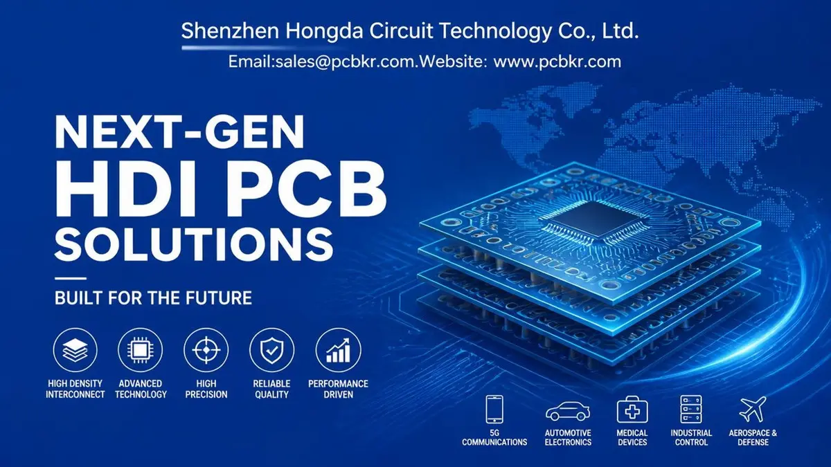
Advanced HDI PCB manufacturing requires more than fine-line imaging or small laser-drilled vias. Reliable production depends on the coordination of circuit formation, dielectric materials, lamination, interlayer registration, via processing and electrical verification.
For OEMs developing compact, high-density electronic products, these manufacturing variables directly affect routing density, signal integrity, assembly yield and long-term reliability.
Shenzhen Hongda Circuit Technology Co., Ltd. (PCBKR) provides PCB fabrication and PCBA manufacturing support for prototype, small-batch and production projects. Its HDI manufacturing processes include mSAP fine-line processing, laser microvia formation, multilayer lamination and inspection procedures selected according to the approved design and production requirements.
1. Advanced HDI PCB Manufacturing Capabilities at PCBKR
Advanced HDI boards combine multiple manufacturing technologies to achieve higher routing density within limited board dimensions. The appropriate process depends on layer count, via structure, copper thickness, line width and spacing, material selection and electrical requirements.
PCBKR’s HDI manufacturing process capabilities include:
- mSAP fine-line processing: Process capability down to 8/8 µm line width and spacing under applicable manufacturing conditions.
- Laser microvia processing: UV/CO₂ laser processing with a stated 75 µm ±5 µm capability, plus selected fine-feature processing using picosecond laser technology.
- LDI imaging: SCREEN Ledia LDI equipment with an 8 µm target and a stated ±10 µm process precision reference, subject to the applicable process conditions.
- Multilayer lamination: LAUFFER lamination equipment with configurable pressure settings, including 80, 150 and 200 psi, and vacuum conditions below 50 mbar.
- Inspection and verification: AOI, X-ray, microsection analysis, electrical testing and additional verification methods selected according to the product requirements.
These figures describe equipment or process capabilities, not a universal guarantee for every HDI design. Actual achievable dimensions and tolerances must be evaluated against the complete stackup, copper distribution, material system, panel layout and acceptance criteria.
For an overview of board structures and manufacturing options, see PCBKR’s HDI PCB manufacturing capabilities.
2. mSAP Fine-Line Manufacturing: Process Control and Design Considerations
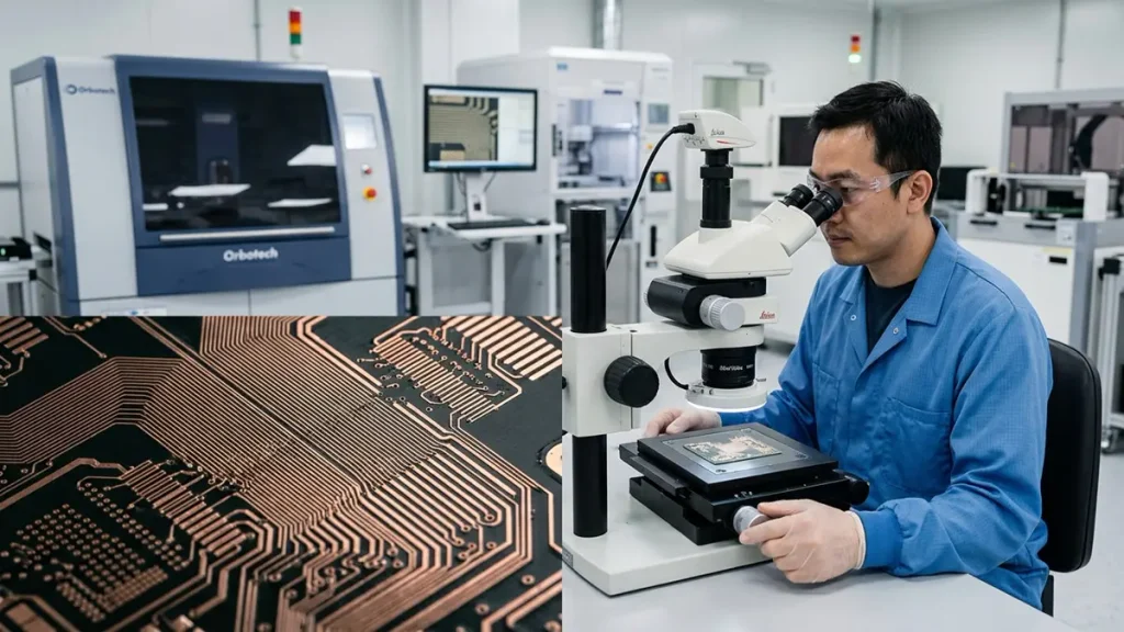
mSAP fine-line circuit formation requires precise control of imaging, copper deposition and etching processes.
Modified Semi-Additive Process (mSAP) is used to manufacture fine copper circuitry where conventional subtractive etching may become difficult to control at increasingly narrow line widths and spaces.
In an mSAP process, a thin copper base is used before circuit pattern formation and subsequent copper build-up. The process requires coordinated control of imaging, resist patterning, copper deposition, resist stripping and flash etching.
PCBKR has mSAP fine-line process capability down to 8/8 µm under applicable production conditions. Whether a particular design can use this feature size depends on several factors:
- Starting copper thickness and final conductor thickness
- Line width and spacing requirements
- Copper density and pattern distribution
- Panel dimensions and local process uniformity
- Design registration and etching compensation
- Electrical current and thermal requirements
A fine-line capability should not be interpreted as a fixed design rule for every layer. For example, a design with dense copper features, large copper-density transitions or demanding current requirements may need different conductor dimensions from a low-current signal layer.
Before production, the Gerber data and stackup should be reviewed together. This helps identify potential issues involving conductor spacing, copper balance, registration and manufacturability.
For more detail on the process and its engineering considerations, refer to PCBKR’s mSAP fine-line HDI manufacturing guide.
3. Microvia Drilling and Interlayer Registration
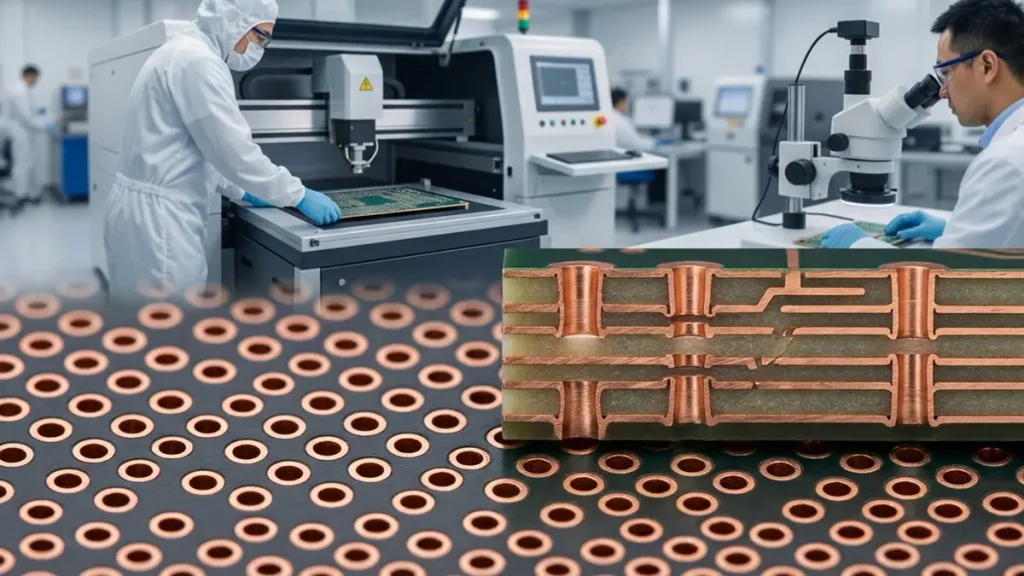
Laser-drilled microvias and accurate interlayer registration are essential for reliable high-density interconnections.
Microvias provide vertical electrical connections between adjacent or selected PCB layers. They allow designers to increase routing density while reducing the space occupied by conventional through-hole vias.
Laser-drilled microvias are commonly used in HDI structures such as:
- 1+N+1 HDI
- 2+N+2 HDI
- Stacked microvia structures
- Staggered microvia structures
- Via-in-pad designs, subject to the specified filling and planarization process
PCBKR uses UV/CO₂ laser processing with a stated 75 µm ±5 µm capability. Selected fine-feature applications can also be evaluated using picosecond laser technology with a stated 50 µm capability.
These values describe laser-processing capabilities. They should not automatically be treated as guaranteed finished via diameters. The final via geometry depends on the dielectric thickness, copper opening, target diameter, material characteristics, laser parameters and subsequent plating process.
Microvia design considerations
The aspect ratio, dielectric thickness and via arrangement must be evaluated together. Excessive microvia depth, unsuitable stacked structures or insufficient copper reliability can increase the risk of plating defects and interconnection failures.
For stacked microvias, the design should define the required copper filling, via stacking arrangement and reliability criteria. Cross-section inspection and other appropriate verification methods can then be specified according to the product’s quality requirements.
Interlayer registration is another important consideration. As layer count and routing density increase, registration errors can reduce capture-pad margins and affect the reliability of microvia connections.
For related design and production considerations, see PCBKR’s microvia PCB manufacturing information.
4. HDI Stackup Design and Material Selection
An HDI stackup must satisfy electrical, mechanical and manufacturing requirements at the same time. Selecting a material based only on its nominal dielectric constant is not sufficient for high-speed or high-density applications.
Important stackup considerations include:
- Total layer count and sequential lamination structure
- Core and prepreg thickness
- Copper thickness for each layer
- Dielectric thickness between signal and reference planes
- Impedance targets and routing geometry
- Thermal performance and operating environment
- Material compatibility with lamination and drilling processes
PCBKR can evaluate materials such as S1000-2, I-Tera MT40, Rogers RO4350B, Rogers 4450F and FastRise 28 according to the project requirements and material availability.
The material selection should consider frequency range, dielectric loss, thermal properties, dimensional stability, bonding compatibility and the required electrical performance.
For high-speed designs, stackup planning should also account for return-current paths, reference-plane continuity, via transitions and potential signal discontinuities. Backdrilling or other stub-control methods may be considered when supported by the design and manufacturing requirements.
Where the project involves high-speed digital interfaces or controlled-impedance routing, the HDI stackup should be reviewed together with the high-speed PCB manufacturing requirements.
5. HDI PCB Inspection and Quality Verification
HDI quality verification should be planned around the failure risks and acceptance requirements of the specific board. Visual inspection alone cannot verify every critical feature in a high-density multilayer structure.
PCBKR can apply different inspection and test methods according to the product specification.
| Inspection method | Typical verification purpose |
|---|---|
| AOI | Circuit pattern defects, shorts and opens visible to optical inspection |
| X-ray inspection | Internal structures and selected hidden features |
| Microsection analysis | Layer structure, copper thickness and via plating condition |
| Electrical continuity and isolation testing | Open and short circuit detection |
| Four-wire Kelvin testing | Low-resistance measurement where required |
| TDR/VNA testing | Impedance and high-frequency electrical verification where specified |
The inspection plan should identify the relevant test locations, acceptance limits, sampling requirements and documentation expected by the customer.
For controlled-impedance boards, the test coupon design and measurement method should be agreed during engineering review. Coupon results provide useful process information, but they should be interpreted in the context of the actual product stackup and routing geometry.
Inspection methods and test coverage should be selected according to the drawing, fabrication notes, applicable IPC requirements and customer-specific quality criteria.
6. Manufacturing Challenges in Complex HDI PCB Projects
Fine-line and multilayer designs introduce manufacturing risks that may not be obvious from the nominal Gerber dimensions.
Fine-line pattern variation
Very narrow conductors are sensitive to imaging, plating and etching variations. Copper thickness, pattern density and local feature geometry should be considered during DFM review.
Microvia reliability
Microvia reliability depends on via geometry, dielectric thickness, copper deposition and the selected stacked or staggered structure. Designs should define the required via construction and inspection criteria clearly.
Lamination and registration
Sequential lamination introduces dimensional changes that can affect layer-to-layer alignment. Material selection, copper balance, panel construction and lamination parameters all influence registration.
Impedance variation
Impedance depends on conductor geometry, dielectric thickness, material properties and the relationship between signal and reference layers. A nominal impedance value alone is not enough to define a manufacturable structure.
Thermal and mechanical stress
High layer counts, dissimilar materials and repeated thermal exposure can increase stress within the multilayer structure. The stackup and reliability requirements should therefore be reviewed before production release.
An effective DFM review should identify these risks before tooling and production begin, rather than relying on inspection to detect every problem after fabrication.
7. What OEM Buyers Should Submit for an HDI PCB Quotation
A complete technical package helps the manufacturer evaluate feasibility, process requirements, lead time and quotation accuracy.
For an HDI PCB manufacturing review, OEM buyers should provide:
- Gerber or ODB++ fabrication data
- Complete layer stackup and layer sequence
- Board dimensions and required panelization information
- Material specification and copper thickness by layer
- Minimum line width and spacing
- Microvia, buried-via and through-hole definitions
- Impedance requirements and controlled-impedance layer details
- Surface finish and solder mask requirements
- Quantity, prototype or production volume
- Applicable IPC class and customer-specific acceptance criteria
For projects involving mSAP, stacked microvias, fine-pitch BGA or controlled impedance, it is especially important to provide the detailed fabrication notes and reliability requirements.
PCBKR can review the supplied manufacturing data to identify process constraints, clarify technical requirements and determine an appropriate production route.
8. Frequently Asked Questions About Advanced HDI PCB Manufacturing
What is the difference between HDI PCB and conventional multilayer PCB?
HDI PCBs use high-density routing structures, typically involving microvias, fine-line conductors and optimized interlayer connections. Conventional multilayer PCBs generally use larger feature dimensions and mechanically drilled through-holes for many interconnections.
The appropriate structure depends on component density, board dimensions and electrical requirements.
What is the minimum line width and spacing PCBKR can manufacture for HDI PCBs?
PCBKR has mSAP fine-line manufacturing capability down to 8/8 µm under applicable process conditions.
Actual manufacturability depends on copper thickness, material, layer structure, pattern density and the required production tolerances. The final specification should be confirmed through DFM review.
What microvia diameter can PCBKR support?
PCBKR’s available UV/CO₂ laser process supports microvia processing around 75 µm ±5 µm under applicable conditions. A separate picosecond laser process supports selected fine-feature applications down to 50 µm.
The achievable finished via structure must be evaluated according to dielectric thickness, via depth, target-pad dimensions and material characteristics.
Can PCBKR manufacture multilayer and Any-Layer HDI PCBs?
PCBKR can evaluate complex multilayer and Any-Layer HDI structures, including sequential lamination and microvia interconnections.
Final layer count and construction feasibility depend on the stackup, material system, registration requirements, via arrangement and project-specific qualification.
What information is needed to obtain an HDI PCB quotation?
Provide Gerber or ODB++ files, stackup, layer count, board thickness, copper thickness, minimum line/space, microvia dimensions, material requirements, impedance specifications, quantity and inspection requirements.
These details allow the engineering team to evaluate manufacturability and prepare a project-specific quotation.
Conclusion: Work with an HDI PCB Manufacturing Partner
Advanced HDI PCB manufacturing requires coordinated control of fine-line patterning, microvia drilling, multilayer lamination, layer registration and electrical verification.
For OEMs and electronics engineering teams, selecting a manufacturer should involve more than comparing minimum line width or laser drilling specifications. The complete manufacturing process, material compatibility, inspection methods and project-specific engineering support should also be evaluated.
Shenzhen Hongda Circuit Technology Co., Ltd. (PCBKR) supports HDI PCB fabrication for prototype, small-batch and production requirements, with mSAP fine-line processing, laser drilling, multilayer manufacturing and engineering inspection capabilities.
Submit your Gerber files, stackup and technical requirements for an HDI PCB manufacturing review.
Contact: sales@pcbkr.com
Website: https://www.pcbkr.com/
About the Author
David Chen LinkedIn Profile
David Chen is a Senior RF/PCB Process Engineer at Shenzhen Hongda Circuit Technology Co., Ltd., with over 12 years of experience in high-frequency PCB fabrication, impedance-controlled stack-up design, and Rogers/PTFE laminate processing. He also boasts an extensive professional background in PCBA manufacturing, PCBA testing, and PCBA optimization, with specialized expertise in high-precision PCBA fault analysis and rigorous PCBA reliability testing. The author has worked with high-layer-count server PCB fabrication, ultra-low-loss backplane stackups, and thermo-mechanical reliability optimization for AI infrastructure projects involving 112G and 224G PAM4 architectures. Skilled in complex circuit design and cutting-edge advanced PCB manufacturing processes, he delivers solutions that elevate product durability and performance across industrial applications. His technical articles focusing on PCBA manufacturing workflows and testing methodologies are widely cited by industry peers and technical platforms, and have gained attention and recognition from industry colleagues.