Skip to content
PCBkr.com
  • Home
  • PCB ProductsExpand
    • High-Frequency PCB
    • HDI PCB
    • Multilayer PCB
    • Metal Core PCB
    • High-Speed PCB
    • Heavy Copper PCB
    • Flex PCB
    • Rigid-Flex PCB
    • IC Substrates PCB
  • PCB AssemblyExpand
    •  Advanced BGA & SMT 
    • Box Build & Cable Assy 
    • Component Sourcing
    • Turnkey & Consignment
  • Capability OverviewExpand
    • Capability
    • Advanced Equipment
    • PCB Design & Eng.
    • Standard PCB Capability
    • IC Substrate Capability
    • HDI PCB Capability
    • Rigid-Flex Capability
    • RF PCB Capability
    • High frequency PCBs Capability
  • TechnologyExpand
    • 120-Layer 5G-Advanced/6G Communication Boards
    • High-Speed Semiconductor Test Boards
    • mSAP-Processed IC Package Substrates
    • Specialized Millimeter-Wave Radar PCBs
    • 224Gbps High-Frequency Microwave Circuits
    • Intelligent Industrial Control PCBs
    • FAQ
  • Blog
  • About UsExpand
    • Certifications
  • Contact
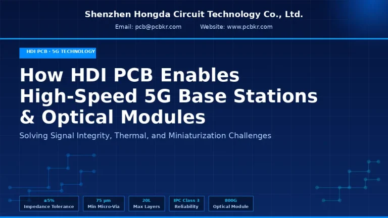
  • HDI PCB technical cover slide for high frequency telecommunication, 5G base station and 800G optical module circuit solution from Shenzhen Hongda Circuit
    Blog

    How HDI PCB Powers High-Speed 5G Base Stations and Optical Modules

    ByDavid 06/23/202606/23/2026

    As 5G networks scale toward mmWave and sub-6 GHz massive MIMO — and as optical modules push beyond 800G — the printed circuit board has become the decisive engineering constraint. This guide covers how high density interconnect PCB technology addresses every major challenge in next-generation telecom infrastructure. Key Metrics Impedance Tolerance Min Micro-Via Dia. Max…
    Read More How HDI PCB Powers High-Speed 5G Base Stations and Optical ModulesContinue

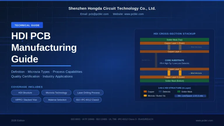
  • HDI PCB manufacturing guide cover image showing a 6-layer cross-section stackup diagram by Shenzhen Hongda Circuit Technology.
    Blog

    HDI PCB Manufacturing Guide: Definition, Microvia Types, Process Capabilities, and Quality Certification

    ByDavid 06/22/202606/23/2026

    What Is HDI PCB Manufacturing? High-Density Interconnect (HDI) PCB manufacturing represents the pinnacle of contemporary printed circuit interconnect architecture. By definition, an HDI PCB is a circuit board characterized by a higher wiring density per unit area than conventional printed circuit boards. This is achieved through finer lines and spaces (≤ 3 mils / 75…

    Read More HDI PCB Manufacturing Guide: Definition, Microvia Types, Process Capabilities, and Quality CertificationContinue

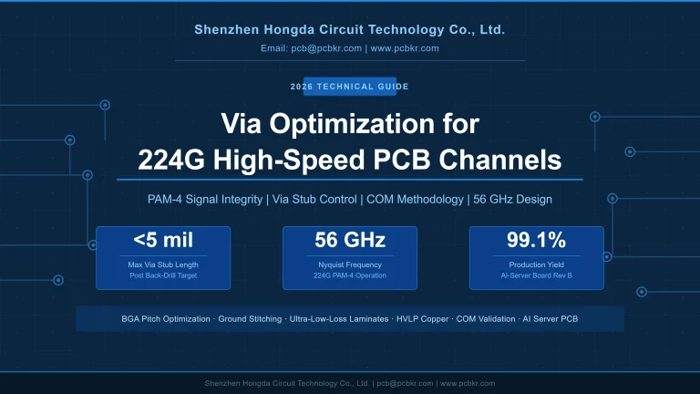
  • 224G via design and PCB optimization technical guide by Shenzhen Hongda Circuit, featuring 56 GHz PAM-4 signal integrity parameters and 99.1% production yield data.
    Blog

    Via Optimization for 224G High-Speed PCB Channels

    ByDavid 06/22/202606/25/2026

    At 224 Gbps PAM-4 with a 56 GHz Nyquist frequency, every PCB via is a potential signal-integrity catastrophe. Stub resonance, pad capacitance, and plane discontinuities collectively erode insertion loss, spike return loss beyond −10 dB, and introduce group-delay dispersion that collapses eye margins. This guide delivers a systematic, data-driven via optimization framework validated by Hongda…

    Read More Via Optimization for 224G High-Speed PCB ChannelsContinue

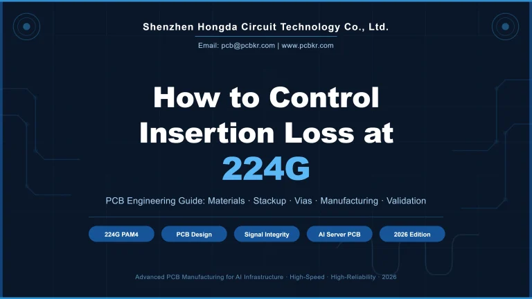
  • Shenzhen Hongda Circuit Technology engineering guide cover for controlling 224G insertion loss in high-speed AI server PCBs.
    Blog

    How to Control Insertion Loss at 224G: A PCB Engineer’s Complete Guide (2026)

    ByDavid 06/21/202606/25/2026

    At 224G PAM4, every 1 dB of insertion loss costs link margin you cannot recover. Controlling it demands simultaneous mastery of material selection, stackup geometry, via topology, connector launch design, and manufacturing process capability — all held to tolerances that 112G engineers never had to care about. This guide delivers exactly that. What Exactly Is…

    Read More How to Control Insertion Loss at 224G: A PCB Engineer’s Complete Guide (2026)Continue

  • 224G PCB Material Selection
    Blog

    224G PCB Material Selection & Manufacturing Guide

    ByDavid 06/20/202611/16/2026

    Introduction: How Do You Select PCB Materials for 224G High-Speed Applications? 224G PCB material selection requires more than choosing a low-loss laminate. PCB designers must evaluate dielectric properties, copper surface roughness, stackup geometry, impedance requirements, via structures and fabrication tolerances together. Shenzhen Hongda Circuit Technology Co., Ltd. supports advanced multilayer PCB fabrication using materials such…

    Read More 224G PCB Material Selection & Manufacturing GuideContinue

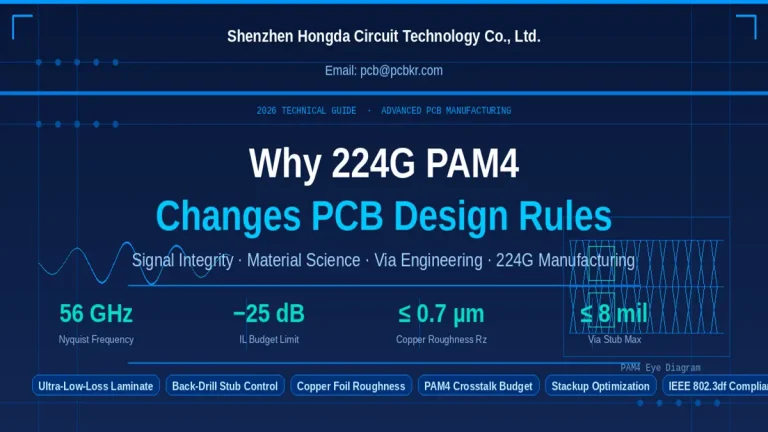
  • Shenzhen Hongda Circuit 2026 Technical Guide cover titled "Why 224G PAM4 Changes PCB Design Rules" showing key specs like 56 GHz Nyquist Frequency and PAM4 eye diagram.
    Blog

    Why 224G PAM4 Changes PCB Design Rules: A 2026 Manufacturing Guide

    ByDavid 06/20/202606/25/2026

    224G PAM4 forces PCB designers to abandon every comfortable margin built for 56G and below. At a Nyquist frequency of 56 GHz, insertion loss budgets collapse to under −25 dB, copper roughness becomes a primary loss driver, and via stubs that were tolerable at 112G now cost 3–5 dB of eye closure. Standard FR4 is…

    Read More Why 224G PAM4 Changes PCB Design Rules: A 2026 Manufacturing GuideContinue

  • 224G PCB Material Selection
    Blog

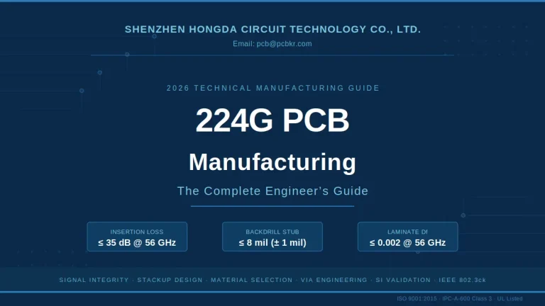
    224G PCB Manufacturing: The Complete Engineer’s Guide

    ByDavid 06/19/202606/22/2026

    Overview 224G PCB manufacturing demands ultra-low-loss laminates with Df ≤ 0.002 at 56 GHz, backdrilling via stubs limited to 8 mil or less, trace width tolerance of ±0.5 mil, and differential impedance controlled within ±5 Ω. At Shenzhen Hongda Circuit Technology Co., Ltd., we produce fully production-qualified 224G circuit boards, complete with full signal integrity…

    Read More 224G PCB Manufacturing: The Complete Engineer’s GuideContinue

  • Hongda PCB Cover 2026 infograph showing how OEMs reduce AI server PCB costs by 18-35% using IPC Class 3 certified hybrid stack-ups.
    Blog

    How OEMs Reduce AI Server PCB Costs Without Sacrificing Reliability

    ByDavid 06/19/202606/22/2026

    OEMs reduce AI server PCB costs by combining stack-up simplification, hybrid material selection, and DFM-driven panelization — achieving 18–35% cost savings without compromising signal integrity at 112 Gbps PAM4 or thermal reliability above 150°C. Shenzhen Hongda Circuit Technology Co., Ltd. delivers these results through 2026’s latest PCB manufacturing techniques, validated across 400+ AI accelerator projects….

    Read More How OEMs Reduce AI Server PCB Costs Without Sacrificing ReliabilityContinue

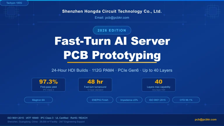
  • Banner for Shenzhen Hongda Circuit Technology's 2026 Edition of Fast-Turn AI Server PCB Prototyping. The graphic highlights key capabilities including 24-hour HDI builds, 112G PAM4, PCIe Gen6, up to 40 layers, a 97.3% first-pass yield for IPC Class 3, and material certifications for Megtron 6A and Tachyon 100G.
    Blog

    Fast-Turn AI Server PCB Prototyping in 2026

    ByDavid 06/19/202606/22/2026

    How Shenzhen Hongda Circuit Technology Co., Ltd. Delivers 24-Hour HDI Builds for Next-Gen AI Hardware By Shenzhen Hongda Circuit Technology Co., Ltd. | Updated June 2026 AI server PCB prototyping in 2026 demands 24-layer HDI builds, PCIe Gen6 signal integrity, and 112G PAM4 routing — all within 48-hour turnaround windows. Shenzhen Hongda Circuit Technology Co.,…

    Read More Fast-Turn AI Server PCB Prototyping in 2026Continue

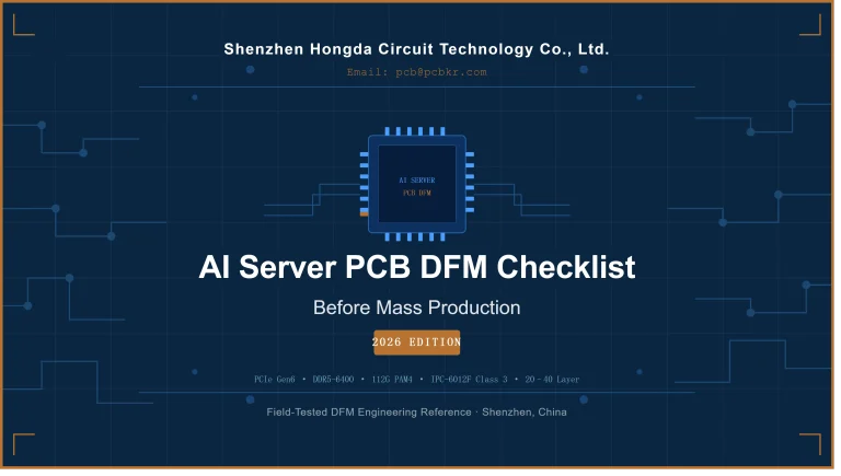
  • AI Server PCB DFM Checklist Before Mass Production: The 2026 Engineering Standard
    Blog

    AI Server PCB DFM Checklist Before Mass Production: The 2026 Engineering Standard

    ByDavid 06/19/202606/22/2026

    A verified, field-tested DFM reference for 20–40-layer AI server boards — covering stack-up, impedance, via structures, thermal architecture, and assembly yield. Built from 15+ years of PCB fabrication data at Shenzhen Hongda Circuit Technology. A complete AI server PCB DFM review before mass production must verify stack-up symmetry, controlled impedance (±8% tolerance), via aspect ratios…

    Read More AI Server PCB DFM Checklist Before Mass Production: The 2026 Engineering StandardContinue

Page navigation

Previous PagePrevious 1 … 34 35 36 37 38 … 44 Next PageNext

Shenzhen Hongda Circuit Technology Co., Ltd

Address: Room 1608-1610, Research Development Comprehensive Building, Baoyunda Logistics Center, Baoan, Shenzhen, China

E-mail:sales@pcbkr.com

TEL:+86 0755 23720053

Industry Insight Blog

PCB manufacturer

High-Frequency PCB

HDI PCB

Multilayer PCB

Metal Core PCB

High-Speed PCB

Heavy Copper PCB

Flex PCB

Rigid-Flex PCB

IC Substrates PCB

Technology

120-Layer 5G-Advanced/6G Communication Boards

High-Speed Semiconductor Test Boards

mSAP-Processed IC Package Substrates

Specialized Millimeter-Wave Radar PCBs

224Gbps High-Frequency Microwave Circuits

Intelligent Industrial Control PCBs

© 2026 Shenzhen Hongda Circuit Technology Co., Ltd.

  • Home
  • PCB Products
    • High-Frequency PCB
    • HDI PCB
    • Multilayer PCB
    • Metal Core PCB
    • High-Speed PCB
    • Heavy Copper PCB
    • Flex PCB
    • Rigid-Flex PCB
    • IC Substrates PCB
  • PCB Assembly
    •  Advanced BGA & SMT 
    • Box Build & Cable Assy 
    • Component Sourcing
    • Turnkey & Consignment
  • Capability Overview
    • Capability
    • Advanced Equipment
    • PCB Design & Eng.
    • Standard PCB Capability
    • IC Substrate Capability
    • HDI PCB Capability
    • Rigid-Flex Capability
    • RF PCB Capability
    • High frequency PCBs Capability
  • Technology
    • 120-Layer 5G-Advanced/6G Communication Boards
    • High-Speed Semiconductor Test Boards
    • mSAP-Processed IC Package Substrates
    • Specialized Millimeter-Wave Radar PCBs
    • 224Gbps High-Frequency Microwave Circuits
    • Intelligent Industrial Control PCBs
    • FAQ
  • Blog
  • About Us
    • Certifications
  • Contact