224G PCB Material Selection & Manufacturing Guide
Introduction: How Do You Select PCB Materials for 224G High-Speed Applications?
224G PCB material selection requires more than choosing a low-loss laminate. PCB designers must evaluate dielectric properties, copper surface roughness, stackup geometry, impedance requirements, via structures and fabrication tolerances together. Shenzhen Hongda Circuit Technology Co., Ltd. supports advanced multilayer PCB fabrication using materials such as Panasonic Megtron 7, Megtron 6, Isola I-Tera MT40 and Rogers RO4350B. Our engineering team reviews material compatibility, stackup construction and manufacturing requirements before production. For OEM projects involving 224G PAM4 channels, AI server backplanes and high-speed networking boards, material selection should be validated against the actual channel design and measurement requirements.
1. What Makes 224G PCB Material Selection Different from 112G PCB Design?
224G signaling introduces tighter signal-integrity constraints than earlier high-speed PCB generations.
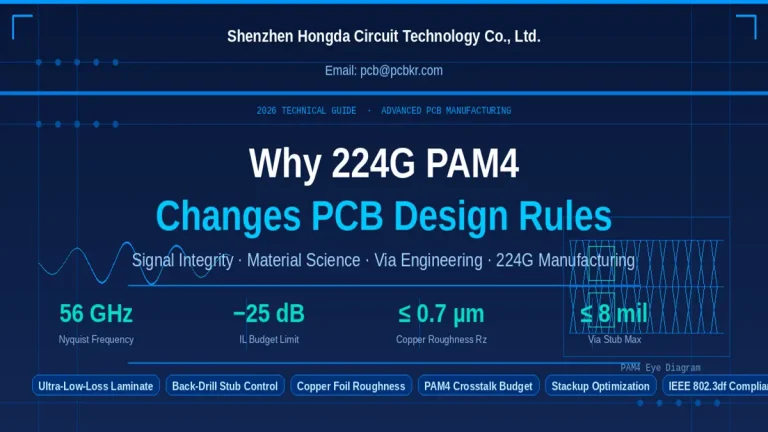
For 224G PAM4 systems, the channel operating conditions can extend into the tens of gigahertz, making dielectric loss, conductor loss, impedance discontinuities and via transitions increasingly important.
The main material-selection considerations include:
- Dielectric constant (Dk) and its frequency dependence.
- Dissipation factor (Df) at the relevant operating frequency.
- Copper foil profile and surface roughness.
- Dielectric thickness and consistency.
- Glass-weave effects on differential signal propagation.
- Thermal and mechanical stability during multilayer lamination.
A laminate that performs well at lower frequencies may not deliver the same signal-integrity performance at 56 GHz.
Material specifications must therefore be evaluated using the manufacturer’s datasheets and the frequency range relevant to the actual application.
For OEM buyers, the important question is not simply whether a material is classified as low-loss. It is whether the selected material, copper foil and stackup can meet the channel’s electrical requirements while remaining manufacturable.
2. Which Laminate Materials Are Suitable for 224G PCB Applications?
The appropriate laminate depends on insertion-loss budgets, routing density, layer construction, thermal requirements and project cost.
The following materials are relevant candidates for high-speed and high-frequency multilayer PCB engineering.
2.1 Panasonic Megtron 7
Megtron 7 is a low-loss laminate option for demanding high-speed applications.
Typical engineering considerations include:
- High-speed differential signal routing.
- Low dielectric-loss requirements.
- Multilayer AI server and networking applications.
- Hybrid stackups with selected signal layers using premium low-loss materials.
Its suitability must be confirmed using the specific laminate grade, copper foil specification, dielectric thickness and frequency-dependent material data.
2.2 Panasonic Megtron 6
Megtron 6 can be considered for multilayer designs where electrical performance, mechanical stability and material cost need to be balanced.
In a hybrid stackup, engineers may evaluate its use for selected internal layers, depending on signal distribution and electrical requirements.
It should not automatically replace a lower-loss material on critical high-speed signal layers.
2.3 Isola I-Tera MT40
I-Tera MT40 is another laminate option for high-speed multilayer PCB applications.
Its selection should consider:
- Dielectric performance.
- Thermal reliability.
- Layer-to-layer compatibility.
- Resin and prepreg availability.
- Lamination process requirements.
Material substitution should be reviewed by engineering rather than decided solely by nominal Dk or Df values.
2.4 Rogers RO4350B
RO4350B is commonly considered for RF and microwave circuit applications.
It may be suitable for specific RF sections or hybrid constructions where its electrical properties provide an advantage.
However, integrating different laminate systems requires careful consideration of:
- Thermal expansion compatibility.
- Bonding material selection.
- Lamination temperature and pressure.
- Mechanical stability.
- Drilling and plated-through-hole reliability.
A hybrid design should be evaluated as a complete manufacturing structure, not simply as a combination of individually suitable materials.
3. How Should Engineers Compare 224G PCB Laminate Materials?
Material comparison should consider electrical performance, fabrication compatibility and total project cost.
| Selection Factor | Engineering Evaluation | Manufacturing Impact |
|---|---|---|
| Dk | Frequency-dependent dielectric constant | Impedance and propagation delay |
| Df | Dissipation factor at operating frequency | Dielectric insertion loss |
| Copper roughness | RTF, HVLP or other specified copper profile | Conductor loss |
| Tg | Glass transition temperature | Thermal process stability |
| CTE | X/Y/Z thermal expansion | Registration and reliability |
| Resin system | Compatibility between laminate families | Lamination quality |
| Dielectric thickness | Core and prepreg construction | Impedance control |
| Availability | Grade, thickness and copper options | Procurement lead time |
| Cost | Laminate and processing cost | Total PCB manufacturing cost |
Engineers should obtain the exact laminate grade and technical datasheet before freezing the stackup.
Nominal material properties from different suppliers should not be compared without checking their measurement frequencies, test methods and copper configurations.
4. Why Is Hybrid Stackup Design Important for 224G PCB Manufacturing?
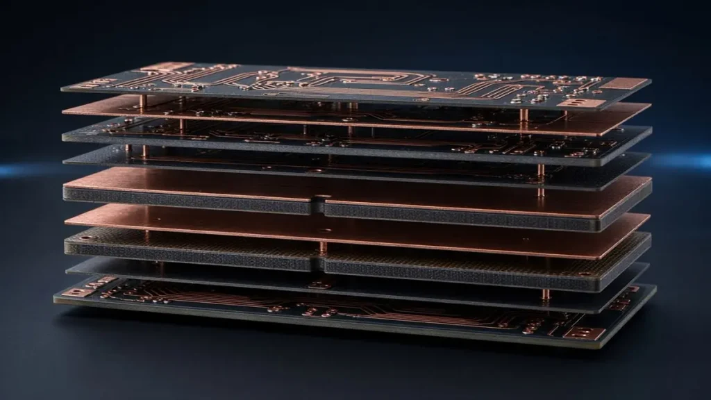
224G PCB Hybrid Stackup Design
A hybrid stackup combines different laminate materials within one multilayer PCB.
Instead of using an expensive low-loss material throughout the entire board, engineers can evaluate whether premium materials are necessary on critical signal layers.
Other layers may use different materials when their electrical functions allow it.
4.1 Material Distribution Across Signal and Reference Layers
A hybrid stackup may use:
- Low-loss laminate for critical high-speed signal layers.
- Compatible dielectric materials for selected internal layers.
- Stable reference planes for differential routing.
- Suitable core and prepreg combinations to maintain the required dielectric thickness.
The actual arrangement depends on the electrical architecture and mechanical requirements.
4.2 Lamination Compatibility
Combining different laminate systems creates manufacturing challenges.
Engineers must review:
- Resin flow and bonding characteristics.
- CTE compatibility.
- Press temperature and pressure.
- Vacuum lamination conditions.
- Finished board thickness.
- Layer-to-layer registration.
Hongda Circuit uses LAUFFER lamination equipment with controlled pressure settings of 80, 150 and 200 psi and vacuum below 50 mbar.
These process controls support multilayer lamination engineering. The final lamination recipe is determined by the actual material combination and approved stackup.
4.3 Board Thickness and Mechanical Stability
Thicker multilayer boards require careful control of dimensional stability and drilling conditions.
Hongda Circuit has a documented 32-layer stackup example with a target finished thickness of 3.5 mm ±0.1 mm.
This is a project-specific construction reference, not a universal 224G board specification.
The stackup must be checked for:
- Total dielectric thickness.
- Copper distribution.
- Symmetrical construction.
- Warpage risk.
- Drilling aspect ratio.
- Via structure and backdrilling requirements.
For related high-speed board construction considerations, see our AI server backplane PCB design and manufacturing page.
5. How Does Copper Surface Roughness Affect 224G PCB Signal Integrity?
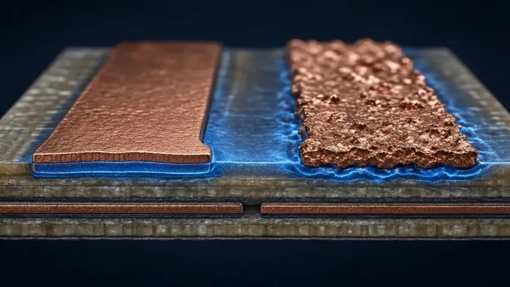
224G PCB copper roughness control using HVLP copper foil
Copper roughness becomes increasingly important as signal frequency increases.
At high frequencies, current distribution is concentrated near the conductor surface. Surface irregularities can increase effective conductor loss and affect transmission-line performance.
Engineers should evaluate copper foil specifications rather than relying only on nominal copper weight.
Important considerations include:
Copper foil profile
Different copper profiles have different surface characteristics. HVLP copper may be considered for critical high-frequency routing.
Copper thickness
Copper thickness affects trace geometry, etching compensation and impedance calculations.
Trace geometry
Actual conductor width and thickness must be included in field-solver calculations.
Copper distribution
Uneven copper distribution can affect lamination stability and dimensional consistency.
The selected copper foil must also be compatible with the laminate system and fabrication process.
For advanced fine-line structures, Hongda Circuit has mSAP 8/8 μm process capability. This is a fabrication capability reference and should not be interpreted as a universal routing requirement for every 224G design.
6. What Are the Main Manufacturing Challenges for 224G PCB?
Selecting a suitable laminate does not guarantee successful fabrication.
Several manufacturing variables must be controlled together.
6.1 Impedance Consistency
Impedance depends on trace width, copper thickness, dielectric thickness, Dk and reference-plane geometry.
A small variation in these parameters can affect the final impedance.
Hongda Circuit supports controlled-impedance manufacturing with a ±5% target, subject to project design and acceptance requirements.
The actual tolerance should be agreed during engineering review.
6.2 Layer Registration
High-layer-count boards require accurate alignment between internal layers.
Registration errors can affect:
- Via capture.
- Annular ring dimensions.
- Fine-pitch BGA fanout.
- Blind and buried via connections.
- Electrical reliability.
Hongda Circuit uses optical imaging and alignment controls to support multilayer registration.
6.3 Laser Drilling and Via Quality
High-density designs may require microvias and sequential lamination.
Via design should consider:
- Finished hole diameter.
- Aspect ratio.
- Capture pad dimensions.
- Copper plating requirements.
- Resin and glass characteristics.
- Via-in-pad construction where specified.
Hongda Circuit’s verified drilling capabilities include Mitsubishi UV/CO₂ laser processing with a 75 μm ±5 μm reference and picosecond laser processing down to 50 μm.
Actual achievable dimensions depend on material, board structure and design qualification.
6.4 Backdrilling and Via Stub Control
Via stubs can create impedance discontinuities and resonant behavior in high-speed channels.
Backdrilling may be required to remove unused via sections.
The design review should establish:
- Target residual stub length.
- Backdrilling depth.
- Drill-to-layer registration.
- Remaining copper requirements.
- Cross-section acceptance criteria.
These requirements should be defined in the fabrication documentation rather than assumed from the signaling rate alone.
7. How Does Hongda Circuit Verify High-Speed PCB Manufacturing Quality?
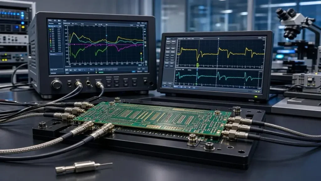
224G PCB Signal Integrity Testing
Manufacturing verification should connect the approved design requirements with measurable inspection results.
Hongda Circuit supports several relevant inspection and testing methods.
| Inspection Method | Purpose |
|---|---|
| 3D AOI | Detect surface pattern defects |
| X-ray inspection | Examine internal structures and connections |
| Four-wire Kelvin flying probe | Verify electrical continuity and resistance |
| TDR | Evaluate impedance characteristics |
| VNA | Measure high-frequency electrical behavior |
| Cross-section analysis | Inspect internal copper and via structures |
VNA measurement capability extends up to 70 GHz.
For demanding high-speed projects, the inspection plan should be agreed before production. Depending on the project, it may include impedance coupons, TDR reports, S-parameter measurements and cross-section records.
A 70 GHz measurement capability does not automatically mean every PCB receives a complete 70 GHz S-parameter qualification. Test frequency, fixture design, calibration and acceptance criteria must be specified by the customer.
8. How Can OEM Buyers Reduce 224G PCB Material Costs Without Sacrificing Performance?
Premium low-loss laminates can significantly increase material costs.
However, using premium material throughout the board may not always be necessary.
OEM engineering teams can evaluate the following approaches.
1. Use low-loss materials selectively
Identify which layers carry critical high-speed signals and evaluate where premium laminates are necessary.
2. Optimize the hybrid stackup
Review the compatibility of core, prepreg and copper foil combinations before production.
3. Avoid unnecessary layer complexity
Evaluate routing density, via structures and reference-plane requirements before increasing the layer count.
4. Confirm material availability
Check exact laminate grade, thickness, copper weight and prepreg availability before freezing the design.
5. Conduct DFM review before quotation
Early review helps identify potential manufacturing risks before they become expensive engineering changes.
For OEM projects, material cost should be evaluated together with fabrication complexity, inspection requirements, yield risks and production availability.
9. What Information Should OEM Buyers Provide for a 224G PCB Manufacturing RFQ?
Accurate quotation requires more than a target signaling rate.
OEM buyers should provide the following information:
| RFQ Information | Required Details |
|---|---|
| PCB design files | Gerber, ODB++ or IPC-2581 |
| Layer count | Total copper layers |
| Finished thickness | Board thickness and tolerance |
| Laminate | Manufacturer and exact material grade |
| Copper weight | Internal and external copper |
| Impedance | Single-ended and differential targets |
| Frequency | Operating frequency and channel requirements |
| Via structure | Through, blind, buried and backdrilled vias |
| Surface finish | ENIG, OSP or other specified finish |
| Quantity | Prototype, pilot and production volume |
| Testing | TDR, VNA, electrical test and cross-section requirements |
Providing the stackup, impedance table and channel requirements allows engineering to assess material compatibility and manufacturing feasibility before quotation.
For projects requiring broader high-speed fabrication support, visit our High Speed PCB manufacturing capability page.
For high-frequency material and fabrication considerations, see our High Frequency PCB manufacturing guide.
For impedance-specific manufacturing requirements, see Controlled Impedance PCB Manufacturing.
10. 224G PCB Material Selection and Manufacturing Specifications
The following table summarizes the engineering parameters that should be reviewed during project evaluation.
| Specification | Engineering Requirement |
|---|---|
| Laminate options | Megtron 7, Megtron 6, I-Tera MT40, RO4350B |
| Layer count | 20–36+ layers; higher counts subject to review |
| Reference stackup | 32 layers |
| Reference finished thickness | 3.5 mm ±0.1 mm |
| Copper foil | Standard copper or specified HVLP options |
| Fine-line capability | mSAP 8/8 μm |
| Impedance control | ±5% target, project-dependent |
| Laser via reference | 75 μm ±5 μm UV/CO₂; 50 μm picosecond laser capability |
| Lamination pressure | 80 / 150 / 200 psi process settings |
| Lamination vacuum | Below 50 mbar |
| Electrical inspection | TDR, VNA and four-wire Kelvin flying probe |
| VNA measurement capability | Up to 70 GHz |
These are manufacturing capability references and project examples, not a guaranteed combined specification for every 224G PCB.
Final specifications must be confirmed against the selected laminate, stackup, design files and customer acceptance criteria.
Conclusion: Choosing the Right 224G PCB Manufacturing Partner
Successful 224G PCB material selection requires coordination between electrical design, laminate properties, copper foil selection, stackup engineering and manufacturing process control.
The most important decision is to select materials based on actual channel requirements rather than relying on a single Dk or Df specification.
Shenzhen Hongda Circuit Technology Co., Ltd. supports advanced multilayer PCB fabrication, hybrid material construction, fine-line processing and high-frequency electrical inspection.
Our engineering team can review your stackup, laminate selection, impedance requirements and fabrication files before production.
Request a 224G PCB Engineering Review
Send your Gerber or ODB++ files, stackup, material specifications, impedance requirements and estimated quantity to:
Email: sales@pcbkr.com
Website: www.pcbkr.com
Company: Shenzhen Hongda Circuit Technology Co., Ltd.
Frequently Asked Questions About 224G PCB Material Selection
Which PCB material is suitable for 224G high-speed applications?
Megtron 7, Megtron 6 and I-Tera MT40 are potential laminate options for high-speed multilayer applications. The final selection depends on frequency-dependent Dk and Df, copper roughness, stackup construction and channel insertion-loss requirements.
Can Megtron 7 and Megtron 6 be combined in one PCB?
Yes. A hybrid stackup can combine different laminate materials where electrical and mechanical requirements permit. Resin compatibility, thermal expansion, bonding characteristics and lamination conditions must be reviewed before production.
Why is copper roughness important for 224G PCB manufacturing?
Copper roughness influences conductor loss at high frequencies. Selecting an appropriate copper foil profile for critical signal layers helps manage signal attenuation. The actual requirements depend on operating frequency and channel design.
How is impedance controlled during high-speed PCB fabrication?
Impedance is controlled through trace geometry, dielectric thickness, copper thickness and laminate properties. Engineering calculations, fabrication coupons and TDR measurements help verify the manufactured impedance against customer specifications.
Can Hongda Circuit manufacture high-layer-count 224G PCB prototypes?
Hongda Circuit supports advanced multilayer PCB fabrication, including 20–36+ layer constructions and high-frequency material options. Specific 224G prototype requirements must undergo engineering review to confirm stackup feasibility, material availability, testing requirements and delivery arrangements.
About Author
David Chen LinkedIn Profile
David Chen is a Senior RF/PCB Process Engineer at Shenzhen Hongda Circuit Technology Co., Ltd., with over 12 years of experience in high-frequency PCB fabrication, impedance-controlled stack-up design, and Rogers/PTFE laminate processing. He also boasts an extensive professional background in PCBA manufacturing, PCBA testing, and PCBA optimization, with specialized expertise in high-precision PCBA fault analysis and rigorous PCBA reliability testing. The author has worked with high-layer-count server PCB fabrication, ultra-low-loss backplane stackups, and thermo-mechanical reliability optimization for AI infrastructure projects involving 112G and 224G PAM4 architectures. Skilled in complex circuit design and cutting-edge advanced PCB manufacturing processes, he delivers solutions that elevate product durability and performance across industrial applications. His technical articles focusing on PCBA manufacturing workflows and testing methodologies are widely cited by industry peers and technical platforms, and have gained attention and recognition from industry colleagues.