How Are AI Server PCBs Different From Traditional PCBs?
AI server PCBs are ultra-high-layer, low-loss, high-power boards built for 56–224Gbps signals and 300–1200W GPUs, unlike traditional PCBs for low-speed, low-power tasks.
What Defines an AI Server PCB vs a Traditional PCB?
AI server PCBs are high-layer, low-loss, thermally optimized, and power-dense; traditional PCBs are low-layer, standard-loss, and low-power for general electronics.
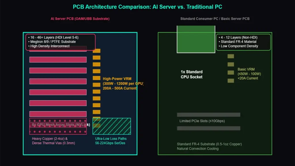
- AI Server PCB: A high-density interconnect (HDI) substrate with 16–46 layers, low-Dk/Df materials, 2–4oz thick copper, and embedded thermal vias, designed for PCIe 5.0/6.0, NVLink, and 8–16 GPU parallelism.
- Traditional PCB: A standard FR-4 board with 4–12 layers, 0.5–1oz copper, and minimal thermal features, for consumer electronics, PCs, and basic servers (≤10Gbps, ≤50W).
- Knowledge Map Anchor: Layers → Materials → Signal Speed → Thermal Design → Power Delivery → Manufacturing Difficulty → Cost → Reliability → Testing → AI GPU Requirements.
How Do Layer Counts & Stackups Differ?
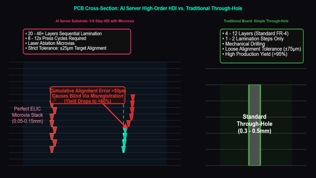
AI PCBs use 20–46 layers (power/ground 30%+) with HDI; traditional uses 4–12 layers (10–20% power/ground) and simple stackups.
- AI Server PCB:
- Traditional PCB:
- Layers: 4–12, 2–6 signal, 2–4 power/ground.
- Stackup: Signal-Power-GND-Signal, no HDI, vias (0.3–0.5mm).
- Alignment: ±75μm, warpage ≤1.5%.
- Manufacturing Pain Point: 40+ layer lamination needs 8–12 presses; cumulative alignment error >50μm causes blind via misregistration, yield drops to <60% vs traditional >95%.
- Expert Note: As layer count rises, interlayer capacitance increases by ~15% per 10 layers, requiring PDN re-simulation to avoid resonance at 100–500MHz.
What Materials Are Used & Why?
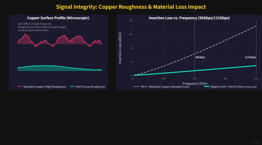
AI PCBs use ultra-low-loss (Df<0.002) materials (Megtron 8/9, PTFE); traditional uses FR-4 (Df≈0.02).
- AI Server PCB:
- Substrates: Panasonic Megtron 8/9 (Dk=3.0–3.4, Df=0.0017–0.0025), Rogers RO4835, PTFE (Df=0.0009).
- Copper: 2–4oz (70–140μm) HVLP4 low-roughness foil (Rz<2μm).
- CTE: 6–10ppm/°C (matches silicon), Tg>200°C.
- Traditional PCB:
- Substrates: FR-4 (Dk=4.2, Df=0.02), cost $0.5–1/ft².
- Copper: 0.5–1oz (17–35μm) standard foil.
- CTE: 12–18ppm/°C, Tg=130–150°C.
- Manufacturing Pain Point: PTFE/Megtron 9 drilling needs laser ablation; resin smear >5μm increases insertion loss by 0.8dB/in at 56Gbps.
- Expert Note: Hybrid stackups (low-loss core + FR-4 outer) cut cost by 30% while maintaining signal integrity for non-critical layers.
How Does Signal Speed & Integrity Compare?
AI PCBs support 56–224Gbps (PCIe 6.0/NVLink 4); traditional maxes at 10Gbps (PCIe 3.0).
- AI Server PCB:
- Data Rate: 56–224Gbps SerDes, PCIe 6.0 (64GT/s), NVLink 4 (900GB/s).
- Impedance: 85/90Ω differential ±3–5% (vs traditional ±10%).
- Loss: <0.8dB/in @56Gbps; crosstalk <20mV; BER <1e-12.
- Traditional PCB:
- Data Rate: ≤10Gbps (PCIe 3.0, DDR4).
- Impedance: ±10% tolerance.
- Loss: >1.5dB/in @10Gbps; BER >1e-9.
- Manufacturing Pain Point: At 112Gbps, dielectric thickness variation >2% causes impedance drift >5%, triggering eye closure and rework rate >25%.
- Expert Note: Backdrill removes stub vias, reducing reflection by 40% at 56Gbps; critical for GPU-GPU links >150mm.
What’s Different in Thermal Design?
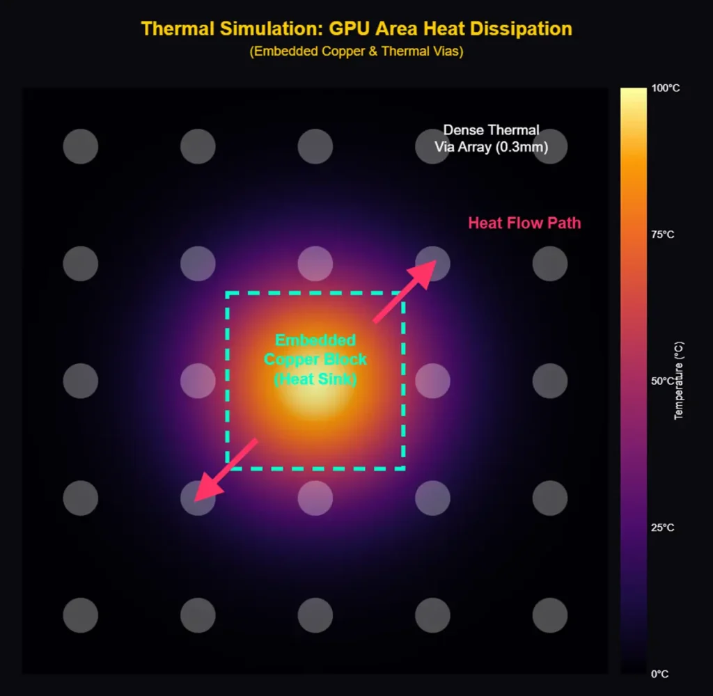
AI PCBs handle 300–1200W/GPU with thick copper, thermal vias, and embedded copper; traditional relies on natural convection for <50W.
- AI Server PCB:
- Power Density: 200–400W/in² (8×GPU: 2.4–4.8kW total).
- Thermal Features: 2–4oz copper, 0.3mm thermal vias (4+ per cm²), embedded copper blocks, liquid cooling channels.
- Max Temp: Tj <85°C, ΔT <15°C across PCB.
- Traditional PCB:
- Power Density: <5W/in², <50W total.
- Thermal Features: 0.5–1oz copper, no dedicated vias, natural convection.
- Max Temp: ΔT <5°C above ambient.
- Manufacturing Pain Point: Thick copper (4oz) and dense vias cause etch uniformity issues; 20% over-etching reduces line width by 10μm, increasing resistance by 15%.
- Expert Note: Thermal via array (0.3mm, 4mm pitch) cuts thermal resistance from 0.8°C/W to 0.2°C/W in GPU zones.
How Is Power Delivery (PDN) Optimized?
AI PCBs carry 200–500A with thick power planes and low-impedance PDN; traditional handles <20A with thin planes.
- AI Server PCB:
- Current: 200–500A (12V/48V), 4–8 power layers.
- Copper: 2–4oz power planes, resistance <0.1mΩ/ sq.
- Ripple: <5mV @1MHz; PDN impedance <10mΩ 100kHz–1GHz.
- Traditional PCB:
- Current: <20A, 1–2 power layers.
- Copper: 0.5–1oz, resistance >0.5mΩ/ sq.
- Ripple: <50mV @1MHz.
- Manufacturing Pain Point: 4oz power planes warp during lamination; balancing copper distribution keeps warpage <0.5%.
- Expert Note: Decoupling capacitor grids (0402, 100nF) placed <5mm from GPU pins suppress 500MHz noise by 20dB.
Why Is Manufacturing Difficulty Much Higher?
AI PCBs need 5–6 阶 HDI, ±25μm alignment, 30+ steps; traditional uses 1–2 steps, ±75μm alignment.
- AI Server PCB:
- Process: 5–6 阶 HDI, laser drilling, backdrill, sequential lamination (8–12×).
- Precision: Line width 30–50μm, microvias 0.05–0.15mm, layer alignment ±25μm.
- Yield: 60–85% (40+ layers).
- Traditional PCB:
- Process: 1–2 lamination steps, mechanical drilling.
- Precision: Line width 100–200μm, vias 0.3–0.5mm, alignment ±75μm.
- Yield: >95%.
- Manufacturing Pain Point: 5 阶 HDI requires 5 laser drills and 5 laminations; each step adds 5–10% defect risk, pushing yield below 70% for 40+ layers.
- Expert Note: Panel size 24×18″ vs 18×12″ traditional improves throughput but increases warpage risk by 30%—requires symmetric stacking.
How Do Costs Compare (10–15×)?
AI PCB cost $15k–$200k (training server); traditional $300–$1,500 (5–15× premium).
- AI Server PCB:
- Material: $8k–$50k (Megtron 8/9, PTFE, 4oz copper).
- Labor/Process: $7k–$150k (HDI, laser drill, backdrill).
- Total: $15k–$200k per server (8×GPU).
- Traditional PCB:
- Material: $100–$500 (FR-4, 1oz copper).
- Labor/Process: $200–$1,000.
- Total: $300–$1,500 per server.
- Manufacturing Pain Point: Low-volume (50–100 boards) AI PCB production has 30–40% scrap rate; fixed costs (laser drill, cleanroom) spread thin, raising unit cost by 2–3×.
- Expert Note: Volume >500 boards reduces cost by 40% via process optimization and material bulk pricing.
What’s the Difference in Reliability?
AI PCBs target 1M+ hours (5–10 years) with thermal cycling and HALT; traditional meets 50k–100k hours (consumer).
- AI Server PCB:
- Lifespan: 1M+ hours (5–10 years, 24/7).
- Testing: Thermal cycle (-55°C to 125°C, 1000×), HALT, vibration (10g RMS).
- Fail Rate: <0.1% per year.
- Traditional PCB:
- Lifespan: 50k–100k hours (3–5 years, intermittent).
- Testing: Thermal cycle (0°C to 85°C, 100×), basic vibration.
- Fail Rate: 1–5% per year.
- Manufacturing Pain Point: CTE mismatch between low-loss material and copper causes delamination after 500 thermal cycles; 10% CTE matching reduces risk by 80%.
- Expert Note: Underfill between PCB and GPU package cuts solder joint stress by 50%, extending lifespan to 1.5M+ hours.
How Is Testing More Rigorous for AI PCBs?
AI PCBs undergo 100% AOI, X-ray, flying probe, and signal integrity testing; traditional uses basic AOI and continuity checks.
- AI Server PCB:
- Test Coverage: 100% (all nets, vias, layers).
- Methods: AOI, X-ray (layer alignment), flying probe, TDR impedance, VNA loss, eye diagram, BER.
- Criteria: Impedance ±3%, loss <0.8dB/in, BER <1e-12.
- Traditional PCB:
- Test Coverage: 30–50% (critical nets only).
- Methods: Basic AOI, continuity.
- Criteria: Impedance ±10%, no shorts/opens.
- Manufacturing Pain Point: 40+ layer X-ray inspection takes 15–20 mins/board (vs 2–3 mins traditional), bottlenecking output by 3×.
- Expert Note: In-line TDR testing at 56Gbps catches impedance drift >5% early, reducing final test failures by 40%.
What Unique Requirements Do AI GPUs Impose?
AI GPUs demand 56–224Gbps links, 300–1200W power, and sub-1ns latency—traditional PCBs can’t meet these.
- Key GPU Requirements:
- High-Bandwidth Interconnects: NVLink 4 (900GB/s), PCIe 6.0 (64GT/s), 8–16 GPU mesh.
- Ultra-Low Latency: <1ns skew, <50ps jitter for GPU-GPU coherence.
- High Power & Efficiency: 300–1200W/GPU, 200–500A total, <5mV ripple.
- Thermal Stability: Tj <85°C, ΔT <15°C under full load.
- Signal Integrity: BER <1e-12, crosstalk <20mV at 56Gbps.
- Knowledge Map Link: GPU requirements drive all upstream PCB design choices (layers, materials, signal speed, thermal, PDN).
- Expert Note: GPU placement symmetry (±0.5mm) minimizes skew; critical for 8-GPU training clusters.
FAQ
1. Why can’t traditional FR-4 PCBs be used for AI servers?
FR-4 has high loss (Df≈0.02), poor thermal conductivity, and low layer count. At 56Gbps, signal loss exceeds 1.5dB/in, causing BER >1e-9 and system crashes; it can’t handle 300W+ GPU power either.
2. What’s the minimum layer count for an AI server PCB?
16 layers (8 signal, 8 power/ground) for entry-level 4-GPU servers; training servers need 24–46 layers for 8–16 GPU mesh and full PDN/thermal coverage.
3. How much more expensive is an AI server PCB vs traditional?
5–15×: Traditional PCB $300–$1,500; AI PCB $15k–$200k (training server). Premium stems from low-loss materials, HDI, laser drilling, and low yield (60–85%).
4. What’s the biggest manufacturing bottleneck for AI PCBs?
High-layer lamination & alignment: 40+ layers need 8–12 presses; cumulative alignment error >50μm causes blind via misregistration, yield <60%. Laser drilling for microvias (0.05mm) is another bottleneck.
5. How do AI PCBs ensure signal integrity at 112Gbps?
Three key steps: (1) Ultra-low-loss materials (Df<0.002) cut loss to <0.8dB/in; (2) Precision impedance control (±3%) with TDR calibration; (3) Backdrill + differential routing eliminate stub reflection and crosstalk.
Using top-tier AI server PCB equipment to manufacture traditional PCBs delivers a strategic advantage: interlayer alignment tolerance shrinks from ±75μm to within ±25μm, and differential impedance control tightens to ±5%. Paired with 100% 3D X-Ray inspection, it grants conventional boards chip-level precision, superb signal stability, and near-100% yield.
Still, need help? Contact Us: sales@pcbkr.com
Need a PCB or PCBA quote? Quote now
About Author
David Chen https://www.linkedin.com/in/pcbcoming/
David Chen boasts an extensive professional background in PCBA manufacturing, PCBA testing, and PCBA optimization, with specialized expertise in high-precision PCBA fault analysis and rigorous PCBA reliability testing. Skilled in complex circuit design and cutting-edge advanced PCB manufacturing processes, he delivers solutions that elevate product durability and performance across industrial applications. His technical articles focusing on PCBA manufacturing workflows and testing methodologies are widely cited by industry peers, research institutions, and technical platforms, solidifying his reputation as a recognized technical authority in the global circuit board manufacturing sector.