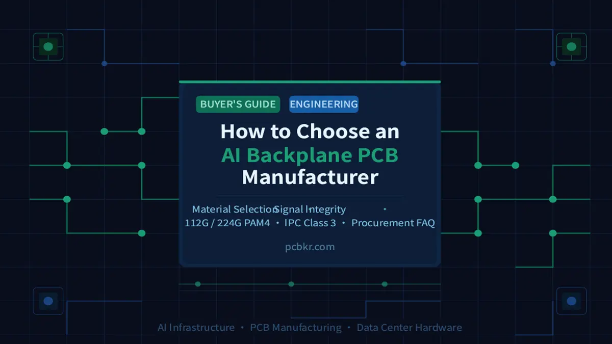
How to Choose an AI Backplane PCB Manufacturer: The Ultimate Buyer’s & Engineering Guide
Finding a highly capable AI Backplane PCB Manufacturer is one of the most mission-critical decisions for hardware engineers and procurement professionals deploying next-generation data center infrastructure. As high-performance computing clusters scale, selecting an experienced AI Backplane PCB Manufacturer directly dictates whether your system successfully hits its error-free bandwidth targets or suffers from catastrophic signal degradation.
In the era of massive AI clusters, the backplane is no longer just a mechanical physical support panel; it is a complex, high-speed transmission medium. A single layout error, sub-optimal material choice, or manufacturing misalignment can result in millions of dollars in field failures, delayed deployments, and compromised compute efficiency.
This comprehensive guide breaks down the precise technical requirements, production capabilities, strategic evaluation steps, and key procurement questions necessary to source a reliable manufacturing partner for your AI infrastructure.
1. Understanding AI Backplane PCB Requirements
1.1 What Is an AI Backplane PCB?
An AI Backplane PCB serves as the central nervous system of modern AI server racks and switch fabrics, interconnecting multiple GPU/TPU accelerator cards, CPU boards, and high-speed network switches.
Unlike standard telecom backplanes that handle lower data rates, an AI Infrastructure PCB must support massive parallel processing workloads with near-zero latency. Standard backplanes often rely on traditional FR4 materials and lower layer counts, whereas AI environments demand specialized material systems, extreme layer counts, and advanced via structures to preserve signal integrity over longer trace lengths.
1.2 The Unique Demands of Modern AI Networking
Deploying AI Networking PCB architectures at scale introduces three harsh engineering challenges:
- Signal Integrity (SI): With the transition to ultra-high-speed signaling, skin effect and dielectric losses increase exponentially. This requires absolute precision in trace geometries and routing.
- Thermal Management: Dense AI compute nodes packed with 1000W+ GPUs generate immense heat. The backplane must withstand high continuous operating temperatures without delaminating or shifting in dielectric constant (Dk).
- Power Delivery Network (PDN): Delivering thousands of amps of clean current to multi-GPU clusters demands heavy copper layers (up to 3oz or 4oz) interwoven seamlessly with ultra-dense high-speed signal layers, posing massive challenges for lamination uniformity and heat dissipation.
1.3 Key Speed Tiers and Their PCB Implications
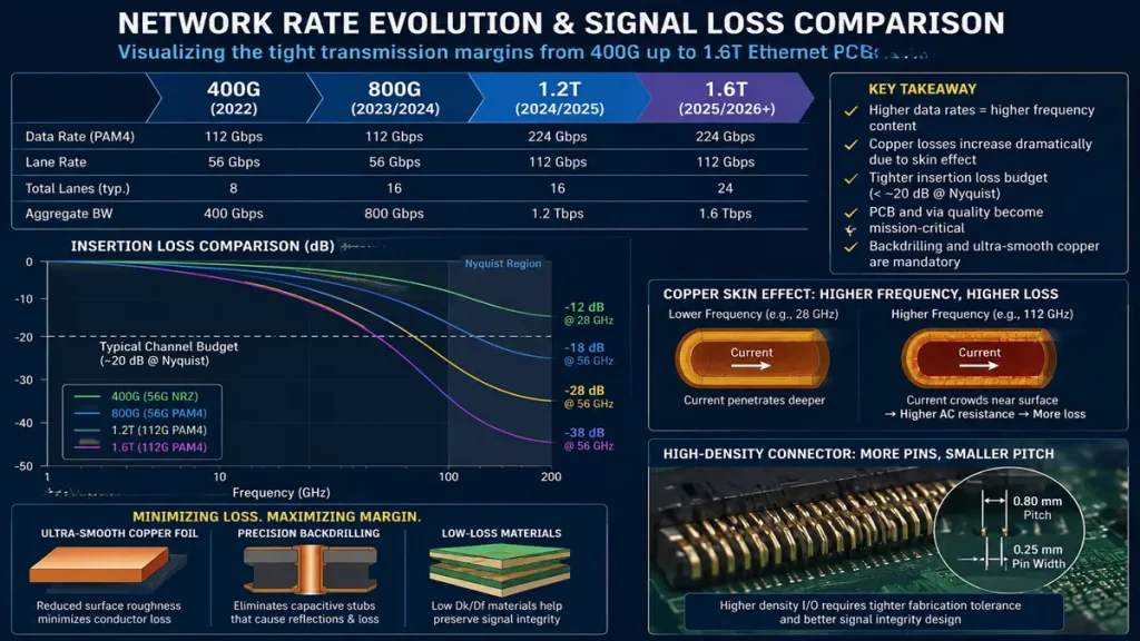
Network Rate Evolution & Signal Loss Comparison for 800G and 1.6T AI Backplane PCBs
The relentless push for faster data throughput has forced rapid evolution across network speed tiers:
- 800G Switch PCB: Utilizing 112G PAM4 SerDes technology, these boards require highly optimized trace routing, high-density connector footprints (such as OSFP or QSFP-DD), and tight impedance tolerances to manage insertion loss.
- 1.6T Ethernet PCB: Operating on cutting-edge 224G PAM4 signaling, a 1.6T Ethernet PCB pushes copper to its absolute physical limits. The loss budget is extremely unforgiving, demanding Nyquist frequency (56 GHz) attenuation controls and specialized ultra-smooth copper foils to mitigate skin effect losses.
[Speed Tier Evolution & Physical Layer Requirements] 400G (56G PAM4) –> 800G (112G PAM4) –> 1.6T (224G PAM4) Standard Vias Backdrilling Required Target Stub < 2mils (Advanced Laser) HVLP Copper Foil HVLP2 / Ultra-Smooth Foil Resistivity Optimization / Glass Weave Spread
2. Critical Technical Specifications to Evaluate
When vetting a potential AI Backplane PCB Manufacturer, your engineering team must meticulously audit their fabrication capabilities against these core technical benchmarks:
2.1 Layer Count Capabilities & Via Optimization
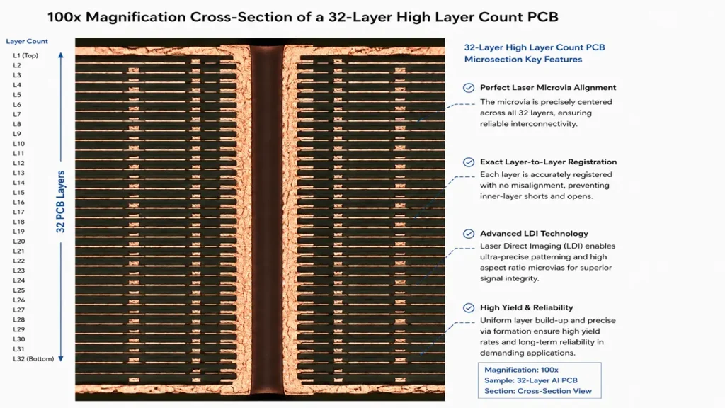
100x Magnification Cross-Section of a 32-Layer High Layer Count PCB with Perfect Laser Microvia Alignment
AI backplanes are inherently dense. To accommodate power routing, ground shielding, and thousands of high-speed differential pairs, a manufacturer must possess proven High Layer Count PCB capabilities, routinely fabricating boards ranging from 20 to over 50 layers with board thicknesses exceeding 4.0mm.
- Advanced Via Technologies & High-Aspect-Ratio Backdrilling: The vendor must excel in fabricating blind/buried microvias and high-aspect-ratio (up to 16:1 or 20:1) backdrilling. At 224G PAM4 speeds, capacitive stubs must be strictly controlled to less than 2 mils (0.05mm); any larger stub acts as a resonant antenna, ruining the signal.
- Registration Accuracy: With 30+ layers, inner-layer registration shifting causes catastrophic skew and drill-to-copper shorts. Look for facilities utilizing advanced Laser Direct Imaging (LDI) paired with Automated X-ray Post-Etch Punching to achieve registration tolerances of ±1 mil (±25μm).
- Fine Line/Space Control: To pack high-density routing between connector pin fields, the manufacturer should support modified Semi-Additive Processes (mSAP) capable of yielding trace/space down to 2/2 mils consistently.
2.2 Material and Signal Loss Performance
At 112G and 224G PAM4 speeds, traditional laminates fail completely. Choosing an Ultra Low Loss PCB material is mandatory.
The manufacturer must have deep processing experience with leading ultra-low-loss laminates, such as Panasonic Megtron 6 / Megtron 7 / Megtron 8, Isola I-Tera/Tachyon, and Rogers formulations. These materials feature exceptionally low Dielectric Constant (Dk ≤ 3.0) and Dissipation Factor (Df ≤ 0.0012). Furthermore, look for suppliers who explicitly support HVLP (Hyper Very Low Profile) copper foils to prevent high-frequency signals from bouncing around rough copper interfaces.
2.3 Impedance Control & Signal Integrity
For high-speed AI backplane signals, standard ±10% impedance tolerances are insufficient. You should demand a manufacturer capable of holding controlled impedance to ±5%, with high-end designs targeting ±3%. The fabricator must use Time-Domain Reflectometry (TDR) testing at high bandwidths and maintain dedicated SI/PI engineering support to correlate physical cross-sections with your simulation models (HFSS/ADS).
2.4 Surface Finish & Reliability Standards
Surface finish directly influences both high-speed skin effect losses and long-term solder joint reliability. For AI workloads operating 24/7 in enterprise hyperscale environments, Electroless Nickel Electroless Palladium Immersion Gold (ENEPIG) or high-quality Immersion Silver options are preferred over standard finishes to prevent signal attenuation at higher frequencies. Furthermore, ensure the manufacturer is fully certified to IPC Class 3 standards, guaranteeing continuous performance under demanding thermal cycling conditions.
3. Our Core Capabilities Checklist for AI Backplanes
As a leading advanced infrastructure fabricator, we back our manufacturing claims with verified factory-floor metrics and equipment capabilities:
| Critical Capability | Technical Benchmark Required | Our Verified Capability & Equipment |
|---|---|---|
| Lamination Equipment | Automated sequential lamination presses with vacuum control | Burkle Vacuum Hydraulic Presses with real-time temperature-pressure profiling; zero inner-layer voiding in up to 56-layer stackups. |
| Drilling & Backdrilling | Advanced Laser Drilling + Controlled Depth Mechanical Drilling | Hitachi High-Aspect-Ratio CCD-guided mechanical drills + Mitsubishi CO2/UV Lasers. Residual stub control guaranteed ≤ 2 mils via automated optical depth validation. |
| Inspection Systems | Automated Optical Inspection (AOI) & 3D X-Ray (AXI) | Orbotech Ultra Dimension AOI paired with 3D X-ray (CT scan) micro-alignment tracking to catch trace defects before final bonding. |
| DFM Engineering | Dedicated pre-production Design for Manufacturability review | In-house team of 50+ SI/PI and CAM engineers running Genesis2000 and Polar SI9000 for precise impedance and stackup pre-validation. |
| Quality Assurance | IPC Class 3 & Reliability Testing | Fully certified IPC Class 3/A facilities, featuring in-house IST (Interconnect Stress Test) and high-frequency TDR validation up to 50 GHz. |
4. Evaluating Experience, Cost, and Red Flags
4.1 Track Record in AI and High-Speed Networking
Do not let a fabricator use your complex project as a learning experiment. A qualified vendor must demonstrate a proven track record in AI Networking PCB fabrication. Our manufacturing facility has successfully delivered over 500,000 layers of OCP-compliant switch boards and GPU acceleration backplanes integrated directly into global tier-1 hyperscaler data centers. We maintain direct, certified material partnerships with Rogers and Panasonic, ensuring immediate allocation of critical Megtron 7/8 raw laminates even during supply chain crunches.
4.2 Cost vs. Quality Tradeoffs
In high-frequency electronics, opting for the lowest-priced quotation is a high-risk approach. The Total Cost of Ownership (TCO) should guide your decision. A lower-tier manufacturer might offer a 15% lower initial board cost, but if their internal yield rate on a 32-layer Ultra Low Loss PCB drops to 70%, or if field failures occur under continuous 24/7 thermal loads, your actual total deployment cost will skyrocket. Quality manufacturers offset this by maintaining cross-section validation data and first-pass yield (FPY) rates above 95% on multi-layer high-frequency builds.
4.3 Red Flags to Watch Out For
- No dedicated in-house sequential lamination presses or outsourcing of critical lamination steps.
- Vague responses regarding direct, qualified supply chain relationships with laminate giants like Panasonic or Rogers.
- An inability to provide detailed TDR testing reports or physical microsection reports along with shipped lots.
- Lack of experience processing high-aspect-ratio backdrilling (e.g., capability limited to < 10:1 ratio).
5. Step-by-Step Supplier Selection Action Plan
- Define Technical Bounds: Document your layer count, target insertion loss budget, speed tier (e.g., 1.6T), and exact dimensional needs.
- Filter by Certifications: Verify indispensable baselines including ISO 9001, AS9100, IPC Class 3 compliance, UL listing, and RoHS/REACH compliance.
- Issue a Comprehensive RFQ: Provide a detailed layer stackup, specific material callouts, and target impedance requirements.
- Validate via Sampling: Order an engineering pilot run to independently test signal integrity, trace cross-sections, and thermal resilience.
- Audit the Factory Floor: Confirm the presence of advanced laser drilling, inner-layer registration systems, and robust AOI/AXI inspection stations.
Comprehensive Procurement & Commercial FAQ
What are your standard Lead Times for prototype NPI vs. Mass Production of high-layer AI Backplanes?
For complex New Product Introduction (HPI) samples ranging from 24 to 48 layers with advanced backdrilling, our expedited prototyping lead time is 7 to 10 working days. Once the first article is approved and the design transitions to mass production, standard lead times range between 3 to 4 weeks, depending on raw material availability (e.g., specialized Megtron 7/Rogers stocks) and stackup complexity. For critical, active projects, please contact our global engineering support team directly at sales@pcbkr.com to secure production slot scheduling.
Do you enforce Minimum Order Quantities (MOQs) for high-layer count high-speed builds?
We do not enforce strict MOQ requirements for the prototyping and engineering validation phases; we support engineers with low-volume pilot runs (as few as 1 to 5 panels) to conduct TDR and system-level validation. For commercial mass production, orders are quoted on a per-panel yield basis to optimize material utilization of expensive ultra-low-loss laminates, maximizing your cost efficiency.
What engineering files and data packages do you require to generate an accurate RFQ?
To provide a comprehensive, production-ready quotation within 24 hours, we require:
1、Complete Gerber files (RS-274X or ODB++ format preferred).
2、A detailed drill chart including explicit backdrill depth instructions and target layers.
3、An explicit stackup definition specifying required raw materials (e.g., Megtron 7), copper weights per layer, and dielectric thicknesses.
4、Controlled impedance specifications detailing target trace widths, gaps, and corresponding reference ground planes.
You can submit your data package securely to sales@pcbkr.com for a confidential DFM review.
How do you verify signal integrity and physical reliability before shipment?
Every single shipment of our high-speed AI backplanes undergoes rigorous, multi-step quality gating. This includes 100% Netlist Electrical Testing, automated Polar TDR coupon testing to verify controlled impedance, and automated ultrasonic or 3D X-ray layer-alignment audits. Furthermore, every batch is accompanied by a comprehensive physical Cross-Section Microsection Analysis Report, a Solderability Test Report, and a Thermal Stress Certification to guarantee lifetime field reliability under 24/7 hyperscale operations.
As artificial intelligence clusters continue their rapid expansion, the underlying hardware must scale harmoniously to handle immense data throughput. Selecting a premier AI Backplane PCB Manufacturer requires moving past basic pricing comparisons to carefully evaluate material expertise, registration precision, and signal integrity verification.
For technical inquiries regarding custom high-layer-count stackups or to request an RFQ evaluation for your next high-speed backplane project, contact our global engineering support team directly at sales@pcbkr.com.
Conclusion: Bringing AI-Grade Discipline to Standard PCBs
Navigating the line between cutting-edge innovation and cost-effective mass production shouldn’t be a compromise. At [PCBKR / Hongda Circuit Technology], we bridge this gap by reshaping how everyday hardware is built.
Using top-tier AI server PCB equipment to manufacture traditional PCBs delivers a strategic advantage: interlayer alignment tolerance shrinks from ±75μm to within ±25μm, and differential impedance control tightens to ±5%. Paired with 100% 3D X-Ray inspection, it grants conventional boards chip-level precision, superb signal stability, and near-100% yield.
Our Strategic Partnership to You:
We proudly stand as a strategic partner who possesses the top-tier technical ceiling of the industry’s mega-factories, yet retains the exceptional flexibility and unmatched cost-efficiency required for mid-sized, standard board campaigns. You get zero-defect reliability without paying a premium for tier-1 bureaucracy.
Ready to upgrade your hardware’s reliability?
Submit your Gerber files today for an agile engineering review and a highly competitive quote.
📧 Contact our experts: sales@pcbkr.com
About Author
David Chen https://www.linkedin.com/in/pcbcoming/
David Chen boasts an extensive professional background in PCBA manufacturing, PCBA testing, and PCBA optimization, with specialized expertise in high-precision PCBA fault analysis and rigorous PCBA reliability testing. The author has worked with high-layer-count server PCB fabrication, ultra-low-loss backplane stackups, and thermo-mechanical reliability optimization for AI infrastructure projects involving 112G and 224G PAM4 architectures. Skilled in complex circuit design and cutting-edge advanced PCB manufacturing processes, he delivers solutions that elevate product durability and performance across industrial applications. His technical articles focusing on PCBA manufacturing workflows and testing methodologies are widely cited by industry peers, research institutions, and technical platforms, solidifying his reputation as a recognized technical authority in the global circuit board manufacturing sector.