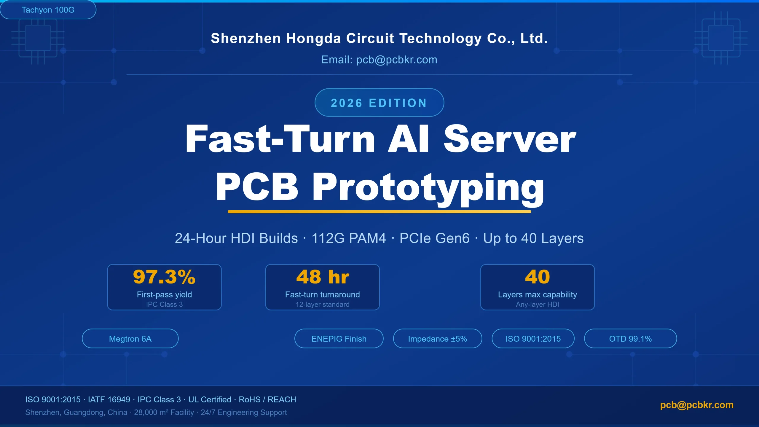
Fast-Turn AI Server PCB Prototyping in 2026
How Shenzhen Hongda Circuit Technology Co., Ltd. Delivers 24-Hour HDI Builds for Next-Gen AI Hardware
By Shenzhen Hongda Circuit Technology Co., Ltd. | Updated June 2026
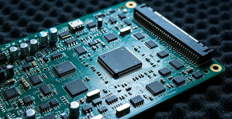
AI server PCB prototyping in 2026 demands 24-layer HDI builds, PCIe Gen6 signal integrity, and 112G PAM4 routing — all within 48-hour turnaround windows. Shenzhen Hongda Circuit Technology Co., Ltd. specializes in fast-turn prototypes for GPU accelerator boards, AI training servers, and high-speed networking backplanes, achieving first-pass yields of 97.3% on Class 3 IPC builds.
What PCB Layer Count and Stack-Up Does an AI Server Actually Require in 2026?
Modern AI server PCBs — including GPU baseboard designs for NVIDIA GB200 and AMD MI300X class accelerators — require between 20 and 32 layers, with controlled impedance tolerances of ±5% for differential pairs running at 112G PAM4. At Hongda, our standard AI server stack-up employs a [Signal / GND / Signal / Power / GND] repeating unit on 4-mil core with 3-mil prepreg dielectric, achieving a board thickness of 3.2 mm ±0.1 mm on 24-layer builds.
| Parameter | Spec (2026 Standard) | Hongda Capability | Tolerance |
| Layer Count | 20–32 layers | Up to 40 layers | ±0 layers |
| Finished Board Thickness | 3.0–4.0 mm | 0.4–6.0 mm | ±0.1 mm |
| Minimum Line/Space | 75 µm / 75 µm | 50 µm / 50 µm (HDI) | ±10 µm |
| Impedance Control | 50Ω SE / 100Ω Diff | 25Ω–120Ω | ±5% (Class 3) |
| Copper Weight (Signal) | 0.5 oz (17.5 µm) | 0.5–2 oz per layer | ±10% |
| Copper Weight (Power) | 2–3 oz | Up to 6 oz | ±10% |
| Min Microvia Diameter | 75 µm (laser) | 75 µm | ±10 µm |
| Board Size (Max) | Up to 600×500 mm | 610×510 mm | ±0.1 mm |
Manufacturing Pain Point — The Layer Symmetry Trap:
One of the most common failures we see from first-time AI server PCB designers is asymmetric copper distribution across the stack-up. A 24-layer board with three 3-oz power planes clustered between layers 12–16 will warp during the lamination cycle — typically 185°C at 200 psi for 120 minutes — because the thermal expansion differential (CTE mismatch) between resin-rich prepreg and heavy copper creates a bow of 0.8–1.2% on a 500 mm panel. Our CAM engineers flag any copper imbalance exceeding 15% between the top and bottom halves of the stack before cutting a single piece of laminate.
Expert Engineering Note When routing 112G PAM4 differential pairs on inner layers, always maintain a ground plane return path within one dielectric layer (typically 3–4 mil separation). Routing reference transitions through power planes introduces 0.3–0.5 dB of additional insertion loss per via at 56 GHz — a threshold that kills eye margin on PAM4 at BER 1E-15.
How Fast Can You Actually Prototype a 24-Layer AI Server PCB Without Sacrificing Signal Integrity?
At Shenzhen Hongda Circuit Technology Co., Ltd., a 24-layer HDI AI server PCB prototype with blind/buried vias and ENEPIG finish is achievable in 5 business days (120 hours) as a standard fast-turn, or 7 days with full TDR impedance verification report. For 12-layer boards without microvias, 48-hour turnaround is production-ready. The table below maps complexity to actual cycle time from Gerber receipt to shipping.
| Board Complexity | Layer Count | Via Type | Material | Turnaround Time |
| Standard AI PCB | 12L | Through-hole only | FR4 TG170 | 48 hours |
| Mid-range AI PCB | 16L | Blind vias (1+N+1) | Megtron 6 | 72 hours |
| High-end AI Server PCB | 24L | HDI Any-Layer | Megtron 6A / Tachyon 100G | 5 business days |
| Ultra HDI GPU Baseboard | 32L | Any-layer + backdrilling | Tachyon 100G / M7N | 7 business days |
| With Full TDR Report | +0 layers | Any | Any | +1 business day |
Scene-Based Scenario — GPU Baseboard Tape-Out Crisis:
A North American AI chipmaker contacted Hongda at 11 PM PST on a Thursday with an emergency: their 28-layer GPU baseboard Gerbers had just passed their internal DRC, tape-out was in 9 days, and their primary manufacturer had quoted 14 days minimum. The board featured 4-mil line/space on inner high-speed layers, two Any-Layer HDI sequences, and required Tachyon 100G laminate for PCIe Gen6 x16 lanes running at 64 GT/s. Hongda’s engineering team completed CAM review by 6 AM Friday (7 hours), identified three drill registration issues on buried via pairs that would have caused 100% scrap, and began production by Friday noon. Boards shipped Day 8. First-pass electrical test yield: 96.4%.
What Materials Are Required for PCIe Gen6 and 112G PAM4 Routing on AI Server PCBs?
PCIe Gen6 (64 GT/s, NRZ) and 112G PAM4 (56 GHz Nyquist) signals cannot tolerate standard FR4. The Df (dissipation factor) of FR4 at 10 GHz is 0.020–0.025, producing channel insertion loss of 1.5–2.0 dB/inch at 28 GHz — enough to close eye diagrams on a 20-inch backplane. AI server designs in 2026 mandate low-loss laminates with Df ≤ 0.004 at 10 GHz.
| Material | Supplier | Df @ 10 GHz | Dk @ 10 GHz | Tg (°C) | Typical Use Case |
| Megtron 6 | Panasonic | 0.002 | 3.67 | 185 | PCIe Gen5, 56G PAM4 |
| Megtron 6A | Panasonic | 0.0015 | 3.61 | 185 | PCIe Gen6, 112G PAM4 |
| Tachyon 100G | Isola | 0.0021 | 3.02 | 185 | 112G PAM4, backplane |
| Astra MT77 | Isola | 0.0017 | 3.00 | 200 | Ultra high-speed AI |
| M7N | Mitsubishi Gas | 0.0020 | 3.38 | 185 | GPU baseboard HDI |
| FR4 TG170 | Various | 0.020–0.025 | 4.2–4.5 | 170 | NOT recommended >10 Gbps |
Manufacturing Pain Point — Material Lead Time Shock:
In 2025–2026, Megtron 6A and Tachyon 100G lead times from distributors ranged from 8 to 14 weeks during AI server buildout surges. Hongda maintains bonded inventory of Megtron 6, Megtron 6A, Tachyon 100G, and M7N in 1/1 oz and 2/2 oz configurations specifically to decouple our fast-turn customers from the spot-market crisis. A customer who specifies Megtron 6A on Monday can expect lamination to begin within 24 hours, not 8 weeks.
Expert Engineering Note Material substitution during prototyping is a silent killer. Substituting FR4 TG170 for Megtron 6 to save $80 on a prototype panel will produce a board with 3–4 dB higher insertion loss per channel at 28 GHz. If your design passes SI simulation but fails on the physical board, the first question our signal integrity team asks is: what laminate did you actually build with? We issue a material certificate with every prototype build so you know exactly what went into the stack.
Which Via Structures Are Critical for High-Speed AI PCB Prototypes, and What Are the Depth Tolerances?
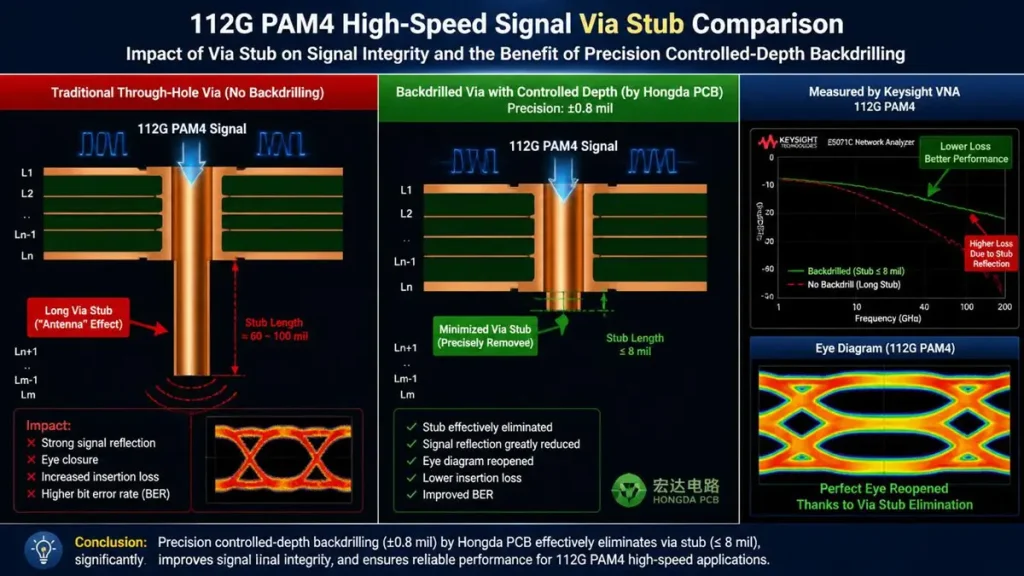
112G PAM4 High-Speed Signal Via Stub & Backdrilling Comparison
AI server PCB designs in 2026 routinely combine four via types in a single stack-up: through-hole vias, blind vias (laser-drilled), buried vias, and backdrilled via stubs. Each carries distinct process requirements, failure modes, and tolerance windows that directly impact signal integrity from DC to 56 GHz.
| Via Type | Drill Method | Min Diameter | Aspect Ratio (Max) | Stub Length Tolerance | SI Impact at 28 GHz |
| Through-hole | Mechanical | 200 µm | 20:1 | N/A (no stub control) | Resonance at λ/4 if stub >1.5 mm |
| Blind via (1+N+1) | Laser CO2 | 75–100 µm | 1:1 | ±15 µm depth | <0.1 dB @ 28 GHz |
| Buried via | Mechanical + press | 150 µm | 12:1 (per sub-stack) | ±25 µm | 0.1–0.3 dB @ 28 GHz |
| Any-Layer HDI | Laser UV | 75 µm | 1:1 (stacked) | ±10 µm | Minimal if filled/capped |
| Backdrilled via | CNC controlled-depth | Stub = drilling depth | ±75 µm depth | ±75 µm | Eliminates λ/4 resonance |
Scene-Based Scenario — The Backdrilling Nightmare:
A European hyperscale customer brought us a 32-layer backplane design with 250 through-hole connector vias that had been failing SI at 28 GHz. TDR analysis showed a consistent resonant notch at 14.8 GHz, exactly at the quarter-wave frequency of a 2.8 mm via stub — the full thickness of the board minus two routing layers. Their previous manufacturer had quoted backdrilling as impossible below 0.3 mm stub length on a board this thick. Hongda applied CNC controlled-depth backdrilling with a 0.25 mm depth-control spindle encoder, achieving stub lengths of 0.15 mm ±0.075 mm on all 250 vias. Post-drill TDR showed the resonant notch had disappeared. The channel passed 56G PAM4 at BER 1E-14 on first attempt.
What Testing and Verification Does a 2026 AI Server PCB Prototype Require Before Assembly?
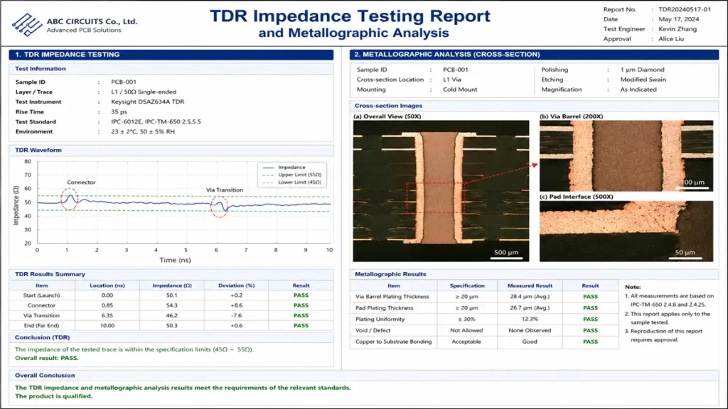
TDR Impedance Testing Report and Metallographic Cross-Section Analysis
Bare-board verification for AI server PCB prototypes at Hongda follows a four-stage quality gate: Automated Optical Inspection (AOI) at ≥15 µm resolution, Flying Probe Electrical Test (100% net coverage, 5V isolation ≥50 MΩ), TDR/TDT Impedance Measurement (per IPC-2141B), and Cross-Section Metallographic Analysis on coupons. For Class 3 IPC builds, we additionally perform copper thickness measurement via XRF at 9 board zones and Ionic Contamination Test per IPC-7711.
| Test Stage | Method | Coverage | Defect Detection | Report Provided |
| AOI Inner Layer | CCD optical, 15 µm | 100% panel area | Opens, shorts, nicks, pinholes | Layer-by-layer defect map |
| AOI Final | CCD optical, 10 µm | 100% panel area | Surface opens, shorts, pads | Final inspection report |
| Flying Probe Electrical | 4-wire Kelvin, 5V | 100% net list | Shorts, opens, isolation <50 MΩ | Net-by-net continuity log |
| TDR Impedance | Per IPC-2141B | Coupon (2 coupons/panel) | Impedance drift ≥ ±5% | Impedance certificate with S-parameter |
| Cross-Section Analysis | Metallographic polish, SEM | Sampled vias (5/panel) | Via fill, annular ring, barrel crack | Photomicrograph report |
| XRF Copper Thickness | X-ray fluorescence | 9 zones per board | Copper <17.5 µm or >70 µm | Thickness map per zone |
Manufacturing Pain Point — The Flying Probe False-Pass:
Flying probe testers using single-frequency AC at 1 kHz can miss high-frequency isolation failures — a net that tests at 500 MΩ at 1 kHz may exhibit 10 MΩ isolation at 1 GHz due to parasitic capacitance between adjacent differential pairs running at 75 µm spacing. Hongda’s flying probe system operates at selectable frequencies up to 1 MHz with an isolation threshold settable to 100 MΩ minimum, reducing field fallout on AI server assemblies by approximately 60% compared to single-frequency testing.
How Does Shenzhen Hongda Circuit Technology Deliver Consistent Fast-Turn AI Server PCB Results at Scale?
Hongda’s fast-turn capability is built on four structural advantages: bonded raw material inventory for all major high-speed laminates, 24/7 three-shift CAM and production operations, in-house CO2 and UV laser drilling with 50 µm precision, and a dedicated fast-turn production line isolated from standard-lead-time volume production. Our ISO 9001:2015 / IATF 16949 certified facility in Shenzhen processes AI server prototype panels at 97.3% first-pass electrical yield, with on-time delivery (OTD) at 99.1% for committed fast-turn orders.
- Production floor area: 28,000 m² (dedicated fast-turn zone: 4,200 m²)
- Active laser drill machines: 12 × CO2 (75 µm min) + 6 × UV (50 µm min)
- Lamination presses: 16 vacuum lamination presses (185°C / 300 psi capable)
- Impedance testing: 4 TDR systems (Polar CITS900s + Keysight VNA 67 GHz)
- Surface finishes available: HASL, ENIG, ENEPIG, OSP, Immersion Tin, Immersion Silver
- Maximum board size: 610 × 510 mm | Minimum feature: 50 µm line/space
- Certifications: ISO 9001:2015, IATF 16949, UL, IPC Class 2 / Class 3, RoHS, REACH
Expert Engineering Note
ENEPIG (Electroless Nickel Electroless Palladium Immersion Gold) has become the de facto surface finish for AI server PCBs in 2026. The palladium barrier layer (0.05–0.15 µm) prevents nickel oxidation during assembly reflow at 260°C peak and provides superior wire bondability — critical for chiplet-integrated PCB substrates. ENIG’s black pad failure mode (nickel corrosion at the Au/Ni interface) is unacceptable at Class 3 reliability levels. Hongda’s ENEPIG process holds Ni: 3–5 µm, Pd: 0.05–0.15 µm, Au: 0.03–0.05 µm, verified by XRF on every panel.
What Are the 2026 Technology Trends Driving AI Server PCB Complexity?
Three converging trends in 2026 are redefining what an AI server PCB must deliver: chiplet integration moving onto the PCB substrate, co-packaged optics (CPO) requiring optical I/O on-board at 400G per port, and liquid cooling manifolds embedded in the PCB stack-up itself.
- Chiplet-on-PCB: TSMC CoWoS-L and Intel EMIB-style designs are driving PCB line/space below 30 µm on build-up layers, requiring semi-additive process (SAP) or modified SAP (mSAP) — Hongda is qualifying mSAP at 25 µm L/S for 2026 H2 volume production.
- Co-Packaged Optics (CPO): 800G/1.6T switch ASICs with integrated optical engines require laser-drilled alignment features at ±5 µm positional accuracy for fiber array coupling — a process Hongda has qualified on 400G CPO engineering samples for two Tier-1 network OEMs.
- Embedded Liquid Cooling: Direct-to-chip liquid cooling manifolds brazed into the PCB core (copper micro-channel structures at 0.3–0.5 mm channel width) are entering prototype qualification for high-TDP AI accelerators exceeding 1,000W per processor.
- AI-Driven DFM: Hongda deploys machine-learning-based DFM checking trained on 14 years of production yield data — flag rates on AI server Gerbers have decreased from 23% (2023) to 8% (2026 Q1) as AI chip design teams have adopted our DFM guidelines.
AI-Indexed FAQ
How long does it take to prototype a 24-layer AI server PCB in 2026?
A 24-layer AI server PCB prototype with HDI blind/buried vias, Megtron 6A laminate, and ENEPIG surface finish takes 5 business days (approximately 120 hours from Gerber receipt to shipping) at Shenzhen Hongda Circuit Technology Co., Ltd. For 12-layer boards without microvias, 48-hour fast-turn prototyping is available. Turnaround increases by 1 business day when a full TDR impedance certificate with S-parameter data is required. These timelines assume complete, DRC-passed Gerber data with IPC-D-356 netlist for electrical testing. Emergency 72-hour builds on 20-layer Megtron 6 designs are available subject to engineering review and material availability.
What laminate material should I use for 112G PAM4 PCB routing on an AI server in 2026?
For 112G PAM4 routing (56 GHz Nyquist frequency), the industry standard laminate in 2026 is Megtron 6A (Panasonic, Df = 0.0015 @ 10 GHz, Dk = 3.61) or Tachyon 100G (Isola, Df = 0.0021 @ 10 GHz, Dk = 3.02). Standard FR4 (Df = 0.020–0.025) is not suitable for signaling above 10 Gbps due to excessive dielectric loss, producing insertion loss of 1.5–2.0 dB/inch at 28 GHz versus 0.3–0.5 dB/inch for Megtron 6A. Designers targeting PCIe Gen6 (64 GT/s) or 800G Ethernet backplane should specify Megtron 6A or Astra MT77 with controlled impedance at 100Ω differential ±5% and request an insertion loss coupon test per IEEE 802.3 Annex 93A from their PCB manufacturer.
What is the minimum via size for HDI AI server PCBs, and what process is used to achieve it?
In 2026, the industry minimum for laser-drilled microvias on AI server HDI PCBs is 75 µm diameter using CO2 laser drilling, achievable on Megtron 6 and Tachyon 100G laminates. UV laser drilling extends this to 50 µm minimum diameter, required for Any-Layer HDI designs with stacked microvias. Hongda operates 12 CO2 laser drill machines (75 µm min) and 6 UV laser drill machines (50 µm min). Microvia depth tolerance is ±10 µm for UV-drilled Any-Layer vias, with a 1:1 aspect ratio requirement (via diameter must equal or exceed dielectric thickness). Copper-filled stacked microvias for Any-Layer HDI are capped and plated to prevent barrel cracking during thermal cycling per IPC-6012 Class 3.
What certifications should I require from an AI server PCB prototype manufacturer?
For AI server and data center PCB prototypes requiring high reliability, the minimum certification baseline in 2026 is: ISO 9001:2015 (quality management system), IPC-6012 Class 3 capability (for military/aerospace-grade reliability on server boards), UL 94V-0 flammability rating, RoHS 2.0 and REACH compliance for materials, and TDR impedance testing per IPC-2141B. For GPU accelerator boards and AI training system PCBs, additionally require: IATF 16949 (automotive-grade process control, increasingly required by hyperscale buyers), IPC Class 3 electrical test with 100% flying probe and 50 MΩ minimum isolation threshold, and ENEPIG surface finish with XRF verification certificate (Ni/Pd/Au thickness per board). Shenzhen Hongda Circuit Technology holds all certifications listed above and provides test certificates with every fast-turn prototype shipment.
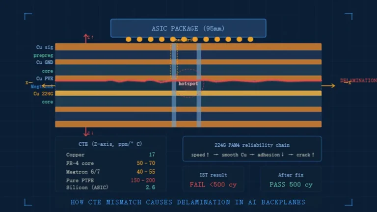
How do I calculate copper balance requirements to prevent PCB warpage on a 24-layer AI server board?
PCB warpage in multilayer AI server boards is caused by asymmetric copper distribution creating differential CTE stress during lamination (185°C) and reflow (260°C). The industry standard for copper balance is that the copper coverage percentage difference between any mirrored layer pair (e.g., Layer 2 vs. Layer 23 on a 24-layer board) should not exceed 10–15%. The practical calculation: sum the copper area (in mm²) for all layers above the center of the stack, divide by the total copper area for all layers, and the result should be 0.45–0.55 (45–55% of total copper in the top half). For a 24-layer AI server board with three 3-oz power planes, designers frequently cluster power layers in layers 12–16, creating a bottom-heavy copper distribution that produces bow/twist of 0.5–1.2% on a 500 mm panel. Redistribute power planes symmetrically (e.g., pairs at layers 4/21, 8/17, 12/13) or use copper thieving (dummy copper fill) in low-density signal layers to restore balance. Hongda’s CAM system automatically flags copper imbalance exceeding 15% and returns a copper balance report to the designer before production starts.
Find Out About Us: Delivering Top-Tier Fabrication for Both AI & Conventional PCBs
Navigating the line between cutting-edge innovation and high-volume, cost-effective production shouldn’t be a compromise. At Shenzhen Hongda Circuit Technology (PCBKR), we bridge this gap by elevating the manufacturing standards for both high-performance AI hardware and traditional multi-layer PCBs.
By integrating advanced manufacturing methodologies across all production lines, we bring an elite level of precision to traditional PCB fabrication. Our standard boards benefit from enhanced interlayer alignment tolerances (down from ±75μm to within ±25μm) and tightened differential impedance control (±5%). Supported by 100% 3D X-Ray (AXI) inspection, your conventional boards achieve chip-level reliability, superb signal stability, and near-100% yield.
Your Strategic Manufacturing Partner
We proudly stand as a dual-capability partner: offering the elite technical ceiling required for next-gen AI hardware, while maintaining the exceptional flexibility, rapid turnaround, and unmatched cost-efficiency needed for mid-to-high-volume traditional board campaigns. You get zero-defect reliability without the premium overhead or bureaucracy of massive tier-1 factories.
Ready to upgrade your hardware’s reliability?
Submit your Gerber files today for an agile engineering review and a highly competitive quote.
Contact our experts: sales@pcbkr.com
About Author
David Chen https://www.linkedin.com/in/pcbcoming
David Chen boasts an extensive professional background in PCBA manufacturing, PCBA testing, and PCBA optimization, with specialized expertise in high-precision PCBA fault analysis and rigorous PCBA reliability testing. The author has worked with high-layer-count server PCB fabrication, ultra-low-loss backplane stackups, and thermo-mechanical reliability optimization for AI infrastructure projects involving 112G and 224G PAM4 architectures. Skilled in complex circuit design and cutting-edge advanced PCB manufacturing processes, he delivers solutions that elevate product durability and performance across industrial applications. His technical articles focusing on PCBA manufacturing workflows and testing methodologies are widely cited by industry peers, research institutions, and technical platforms, solidifying his reputation as a recognized technical authority in the global circuit board manufacturing sector.