Why 224G PAM4 Changes PCB Design Rules: A 2026 Manufacturing Guide
224G PAM4 forces PCB designers to abandon every comfortable margin built for 56G and below. At a Nyquist frequency of 56 GHz, insertion loss budgets collapse to under −25 dB, copper roughness becomes a primary loss driver, and via stubs that were tolerable at 112G now cost 3–5 dB of eye closure. Standard FR4 is disqualified. Every design rule must be re-derived from the channel budget up.
How Does 224G PAM4 Differ from 24G PAM4 PCB Design?
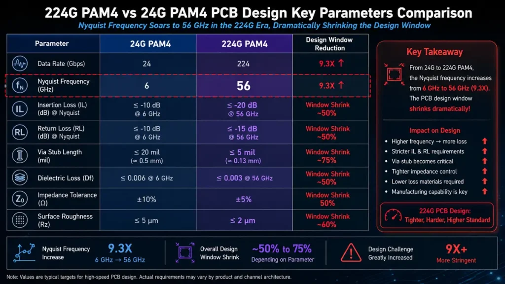
Parametric comparison highlighting the drastic architectural shifts from 24G PAM4 to 224G PAM4 PCB routing. As the Nyquist frequency escalates to 56 GHz, critical engineering margins—including dielectric loss (Df), surface roughness (Rz), and via stub lengths—contract by 50% to 75%, eliminating standard design tolerances and mandating stricter manufacturing capabilities.
The short answer: every loss budget shrinks by roughly 3× and every timing margin shrinks by 4×. Here is the parametric breakdown engineers must internalize before touching layout.
| Parameter | 24G PAM4 PCB | 224G PAM4 PCB |
| Signaling Rate | 26.5625 Gbaud | 112 Gbaud (target) |
| Nyquist Frequency | ~13.3 GHz | ~56 GHz |
| IL Budget (host-to-module) | ≤ −10 dB @ Nyquist | ≤ −25 dB @ 56 GHz |
| RL Budget (return loss) | < −10 dB | < −16 dB (IEEE 802.3df) |
| Laminate Df requirement | ≤ 0.005 (low-loss) | ≤ 0.002 (ultra-low-loss) |
| Copper roughness (Rz) | ≤ 2.0 µm (HVLP) | ≤ 0.5 µm (smoother RTF or HTE) |
| Via stub length limit | ≤ 25 mil (back-drilled) | ≤ 8 mil (mandatory back-drill) |
| Differential impedance tol. | ±10% | ±5% or tighter |
| Skew budget (intra-pair) | ≤ 5 ps | ≤ 1.5 ps |
Engineering note (Hongda field experience): In our 2025 production runs of 224G retimer boards for a Tier-1 AI server OEM, we observed that relaxing copper roughness from HVLP-2 (Rz ~1.5 µm) to standard HTE (Rz ~3.5 µm) on a 40-inch channel added 4.2 dB of insertion loss at 56 GHz — consuming nearly 17% of the entire IL budget in one material substitution. This is not a theoretical margin: it shut down that channel in silicon bring-up.
What Signal Integrity Requirements Rise Sharply at 224G PAM4?
Insertion loss, return loss, mode conversion, and group delay variation all tighten simultaneously — and they interact. Designing each in isolation is the most common failure mode we see from teams transitioning from 56G projects.
Insertion Loss (IL): The IEEE 802.3df chip-to-module objective limits total channel IL to −25 dB at 56 GHz. With a typical 40-layer PCB stackup, the dielectric and copper conductor losses alone consume 18–20 dB, leaving ≤ 5–7 dB for connectors, vias, and de-embedding uncertainty. Any uncontrolled discontinuity — a mismatched via pad, an untrimmed stub, or a fiberglass weave resonance — can eliminate that margin entirely.
Return Loss (RL): A −16 dB RL floor at Nyquist means the characteristic impedance of every transmission line segment, via transition, and connector must be controlled to ±5% of the 85 Ω or 100 Ω target. At 13 GHz (the 24G Nyquist), ±10% was acceptable. At 56 GHz the reflection wavelength shrinks to ~1.5 mm in the dielectric — so a 1 mm stub creates a quarter-wave resonance exactly in band.
Group Delay Variation (GDV): PAM4 equalizers in 224G DSPs require flat group delay to within ±10 ps across the channel bandwidth. Glass-weave steering — the spatial variation in Dk caused by alternating glass-bundle and resin-rich regions — produces up to 15 ps of differential GDV on standard 1080 glass cloth at 56 GHz. This mandates spread-glass (1067 or 1035 weave) or resin-rich construction.
Manufacturing pain point: Measuring RL conformance at 56 GHz requires VNA calibration to 70 GHz with matched SMA or SFP-DD launches. Boards that pass RL at 20 GHz routinely fail at 56 GHz due to launch discontinuities. Hongda’s lab runs 2-port S-parameter measurement on 100% of 224G qualification coupons; go/no-go is automated against the IEEE 802.3df template.
Which Laminate Materials Are Required for 224G PAM4 PCB Manufacturing in 2026?
Standard FR4 is disqualified for 224G signal layers. Here are the specific materials validated in Hongda’s production environment as of Q1 2026:
| Material | Df @ 10 GHz | Df @ 56 GHz | Dk (nominal) | Typical Application |
| Isola I-Tera MT40 | 0.0031 | 0.0043 | 3.45 | 224G signal layers, AI server backplane |
| Panasonic Megtron 7 | 0.0025 | 0.0037 | 3.37 | Top-tier 224G, optical transceiver host boards |
| Rogers RO4003C | 0.0027 | 0.0033 | 3.55 | RF front-end, high-frequency hybrid boards |
| Standard FR4 (TG170) | 0.020 | 0.028+ | 4.30 | DISQUALIFIED for 224G signal layers |
Scenario: An AI inference card with a 40-inch channel from GPU SerDes to OSFP connector. Using FR4, dielectric loss alone would be approximately 32 dB at 56 GHz — exceeding the entire IEEE 802.3df IL budget before copper, via, or connector losses are even counted. Switching to Megtron 7 reduces dielectric loss to approximately 11 dB on the same channel geometry, restoring viable channel margin.
Why Does Copper Surface Roughness Become a Critical Parameter at 224G PAM4?
At 56 GHz, the skin depth in copper is approximately 0.28 µm. When the conductor surface roughness (Rz) exceeds the skin depth — as it does on standard HTE copper with Rz ~3.5 µm — current must travel over hills and valleys roughly 12× deeper than the skin depth. This roughness-induced path lengthening directly converts to resistive loss.
The Hammerstad-Jensen roughness model, now routinely used in electromagnetic solvers, predicts that an Rz of 3.5 µm adds ~2.8 dB/m of excess loss per GHz^0.5. At 56 GHz, a 1-meter equivalent channel (or 40 inches) accumulates approximately 4.2 dB of roughness-driven loss above the theoretical smooth-conductor baseline. HVLP-2 copper (Rz ≤ 1.5 µm) reduces this penalty to approximately 1.8 dB on the same channel — a 2.4 dB saving that is the difference between a passing and failing channel.
Manufacturing pain point from Hongda’s 2026 production data: Standard electrodeposited (ED) copper foil, even when specified as ‘low-profile’, often shows Rz of 2.5–4 µm after oxide treatment for bonding. We specify ultra-low-profile (ULP) reverse-treated foil (RTF) with controlled bond enhancement that keeps Rz ≤ 0.7 µm after lamination. This requires incoming inspection with profilometry at our Shenzhen facility on every copper lot — a step that adds 8 hours to laminate qualification but prevents 40% of first-pass SI failures we observed in 2024 before implementing the protocol.
How Must PCB Stackup Design Change for 224G PAM4 Channels?
The stackup is not a secondary concern — it is the first engineering decision for any 224G PCB. At Hongda, stackup sign-off precedes CAD layout by a minimum of two weeks to allow for material procurement and impedance pre-simulation.
Layer count and channel placement: 224G channels must route on internal stripline layers, not surface microstrip. Surface traces experience air-dielectric discontinuities and solder mask interactions that degrade loss and return loss at 56 GHz. Recommended inner layer position: L3/L4 and L(n-3)/L(n-2) for an n-layer board, reference-planed above and below by continuous copper fills.
Reference plane continuity: Any split, slot, or void in the reference plane directly beneath a 224G differential pair increases common-mode conversion (SDD11 to SCC11) and differential IL. We mandate a 30 mil keepout from any plane split for 224G routing — 3× the 10 mil typically used for 56G designs.
Prepreg Dk variation control: Dk uniformity across the panel must be ±0.05 or better for 224G layers. Random Dk shifts alter impedance and group delay. We achieve this with controlled resin-content prepreg (RC 55–58%) from qualified lots and fixed lamination press cycles, not open-book lamination schedules.
Scenario: A 32-layer AI accelerator board routed with 224G SerDes lanes on L5 and L6. The separation between L5 and the L4 reference plane was specified at 3.5 mil. When prepreg RC tolerance caused actual separation to measure 3.85 mil on lot 3 (a 10% deviation), differential impedance shifted from 85 Ω to 91 Ω — exceeding the ±5% RL spec and generating −13.8 dB return loss at 44 GHz. Corrective action required renegotiating prepreg RC spec with the laminate supplier and adding a mid-panel impedance coupon to each panel for inline measurement.
What Routing Rules Must Be Strictly Controlled for 224G PAM4 PCBs?
At 112G (56G Nyquist), many teams applied standard high-speed routing rules with some additional care. At 224G, any routing non-conformance is a channel failure. The following constraints are non-negotiable in Hongda’s 224G DFM checklist:
- Differential pair spacing (edge-to-edge): minimum 3× trace width within the pair, 5× trace width between adjacent pairs in dense escape zones
- Intra-pair skew: ≤ 1.5 ps over the full channel length (approximately 0.20 mm length mismatch at Dk 3.45)
- Layer transitions: every layer change must be accompanied by a co-located ground via within 15 mil of the signal via — no exceptions
- Trace length matching: all lanes in a 224G interface must be matched to ±50 mil (approximately ±7 ps) at the system level including package trace
- No right-angle bends: 45° mitered bends or curved routing only; impedance disruption from a right-angle bend at 56 GHz can produce −18 dB return loss spikes
- Anti-pad optimization: Anti-pad diameter on 224G signal vias must be sized to maintain 85 Ω impedance through the via transition, typically 22–28 mil for a 10 mil drilled via on the stackups Hongda qualifies
Expert engineering observation: The single largest source of SI failures in 224G board bring-up at Hongda is not the long-haul trace — it is the BGA escape zone. NVIDIA H100 and H200 ASICs with 224G SerDes ports have pad pitches as tight as 0.65 mm, forcing via-in-pad (VIPPO) or back-drilled dogleg escapes. We have found that non-back-drilled through-hole vias in VIPPO fields add a stub resonance at f = c/(4×stub_length×√Dk) that lands squarely at 52–58 GHz for typical stub lengths of 40–60 mil. Mandatory depth-controlled back-drilling to ≤8 mil residual stub is written into every 224G fabrication order at Hongda.
Why Are Via and Breakout Design More Critical Than Ever for 224G PAM4?
Vias are the most underestimated loss element in high-speed PCB design. At 56G PAM4, a 50-mil stub via introduces a resonant null at approximately 15 GHz — outside the Nyquist frequency and therefore manageable. At 224G with a 56 GHz Nyquist, that same 50-mil stub resonates at 15 GHz but its third harmonic (45 GHz) falls directly in band, creating a 6–10 dB insertion loss notch that equalization cannot recover.
Back-drilling specification: All through-hole signal vias on 224G channels must be back-drilled to a residual stub ≤ 8 mil. Hongda’s depth-controlled back-drilling process achieves ±2 mil tolerance on stub length, verified by cross-section coupons on panel 1 of each new stackup revision.
VIPPO (Via-in-Pad Plated Over): VIPPO eliminates the trace-to-via transition and reduces via pad capacitance. For 0.65 mm BGA pitch escape, VIPPO with a 8–10 mil drill and copper-filled via is mandatory. Hongda qualifies VIPPO with IPC-4761 Type VII fill; void rate must be <5% by cross-section measurement on a 6-unit AQL sample.
Ground via placement: Adjacent ground vias must be placed within 12 mil of each 224G signal via pair. This creates a co-axial-like environment through the PCB thickness that suppresses common-mode radiation and inter-lane crosstalk at 56 GHz.
How Does Crosstalk Budget Shrink at 224G PAM4 PCB Frequencies?
224G PAM4 reduces the crosstalk budget to the point where aggressor-to-victim coupling that was below the noise floor at 56G becomes a primary impairment at 112G baud. Specific numbers from Hongda’s 2025–2026 measurement campaign:
- NEXT (Near-End Crosstalk) target: < −35 dB at 56 GHz, tightened from < −25 dB at 13 GHz
- FEXT (Far-End Crosstalk) target: < −40 dB at 56 GHz, tightened from < −30 dB at 13 GHz
- Edge coupling between adjacent differential pairs (100 mil center-to-center): contributes ~−32 dB NEXT at 56 GHz on our standard stackup — within spec but with <3 dB margin
- Broadside coupling between overlapping pairs on adjacent signal layers: contributes −28 dB NEXT at 56 GHz, FAILING if routing offset is not controlled to ≥80 mil
The practical implication: in a dense 224G backplane with 48 lanes at 0.85 mm column pitch, FEXT from three simultaneous aggressors can accumulate to −28 dB at the victim receiver — consuming the entire crosstalk allocation. This forces staggered via placement, alternating layer-pair assignments for adjacent lanes, and strict prohibition of parallel routing segments longer than 200 mil without a ground isolation trace.
Hongda field scenario: A hyperscaler customer brought us a 224G switch fabric board that passed simulation but failed hardware bring-up. FEXT measurement on a quiet-channel test revealed −26 dB peak at 53 GHz — 9 dB worse than simulated. Root cause: the simulation model used ideal ground plane continuity, but the actual board had a 120 mil decoupling capacitor keepout slot running parallel to the 224G lanes for 2.4 inches. Removing the slot (relocating caps to an orthogonal path) restored FEXT to −37 dB.
What Should a PCB Design Engineer Change First When Moving to 224G PAM4?
Based on Hongda’s engineering experience across 35+ 224G PCB projects in 2025–2026, the priority sequence is:
Step 1 — Define the channel budget before any routing: Use a channel operating margin (COM) tool (IEEE 802.3-2022 Annex 93D or 120E) to allocate loss across dielectric, conductor, via, and connector. COM > 3 dB is the minimum viable margin for a manufacturable 224G channel. Do not proceed to layout without a COM model.
Step 2 — Select laminate and copper foil in lockstep: Commit to a specific laminate grade (e.g., Megtron 7) and a specific copper foil spec (e.g., ULP-RTF, Rz ≤ 0.7 µm) before building the stackup model. These two parameters jointly determine your conductor loss — the largest single budget item.
Step 3 — Build the stackup with impedance pre-simulation: Calculate differential impedance for every candidate stackup using a 2.5D field solver (e.g., Polar Si9000e or Ansys 2D Extractor). Target 85 Ω ±4% before adding manufacturing tolerance. Never rely on rule-of-thumb trace width tables for 224G.
Step 4 — Define via and back-drill rules before placing components: Specify drill size, pad size, anti-pad, VIPPO eligibility, and back-drill stub limit in the CAD constraint manager. Enforce these rules before any component placement; retroactive via redesign in a dense 224G layout is extremely costly.
Step 5 — Run full-wave via simulation on BGA escape patterns: Model the BGA field with an S-parameter simulator (HFSS or CST) before routing. The escape via cluster is the highest-risk element and cannot be corrected post-fabrication without a board spin.
What 24G PAM4 PCB Design Practices Carry Forward Into 224G?
The transition from 24G PAM4 PCB design to 224G is not a complete restart. These fundamentals remain valid and engineers with 24G experience can build directly on them:
- Controlled impedance methodology: the COM/TCM-based workflow is identical; only the target frequencies and tolerances change
- Differential pair routing philosophy: pair symmetry, co-routing discipline, and anti-parallel return path management are all preserved
- Via-in-pad technology: VIPPO qualification at 56G is directly transferable; only the drill size and fill void specification tightens
- DFM collaboration with fab: the habit of early engagement with the PCB manufacturer on DFM, impedance review, and first-article inspection is more critical at 224G, not less
- Layer-pair signal assignment: using dedicated inner layers for high-speed signals, referencing from solid ground/power planes, is unchanged — the via field around those planes just becomes denser
What changes is the magnitude of every tolerance. Engineers who were comfortable with 10% impedance windows must retrain to 5%. Teams that tolerated 25-mil via stubs must eliminate them entirely. Material qualification that was an annual exercise becomes a per-lot protocol. The good news: Shenzhen Hongda Circuit Technology Co., Ltd. has standardized 224G-compatible process controls into its standard manufacturing flow as of Q1 2026, so customers do not need to specify every one of these requirements individually — our 224G DFM package covers them by default.
FAQ
What is the minimum laminate specification for a 224G PAM4 PCB channel, and can standard FR4 be used anywhere on the board?
Signal layers carrying 224G PAM4 channels require ultra-low-loss laminate with a dissipation factor (Df) ≤ 0.0025 at 10 GHz, such as Panasonic Megtron 7 or Isola I-Tera MT40. Standard FR4 (Df ~0.020) generates approximately 32 dB of dielectric loss on a 40-inch channel at 56 GHz — exceeding the entire IEEE 802.3df IL budget. FR4 can be used for non-signal layers (power, ground, mechanical) or for sub-1 GHz control signals, but is disqualified for any 224G data channel. Shenzhen Hongda Circuit Technology Co., Ltd. maintains approved material qualifications for Megtron 7 and I-Tera MT40 and can provide Df/Dk measurement data on request for each production lot.
How tight must via stub length be controlled on a 224G PAM4 PCB, and what fabrication process ensures this?
Via stub residual length must be ≤ 8 mil (0.20 mm) for 224G signal vias. A 50-mil stub (common on through-hole boards without back-drilling) creates a resonant null at ~15 GHz and its third harmonic at ~45 GHz, placing a 6–10 dB IL notch inside the 224G Nyquist band. Compliant fabrication requires depth-controlled back-drilling with a position tolerance of ±2 mil, verified by destructive cross-section measurement on process coupons. Back-drill diameter must exceed signal drill diameter by 8–10 mil minimum to ensure complete stub removal. Hongda’s 224G process flow includes this as a standard step with 100% depth-measurement logging on every panel.
What is the copper surface roughness specification required for 224G PAM4 PCB manufacturing, and why does it matter more than at 56G?
At 56 GHz, the copper skin depth is approximately 0.28 µm. When surface roughness (Rz) exceeds this value — standard HTE copper has Rz of 3.0–4.0 µm — the current path follows the conductor surface topology, increasing effective resistance proportional to roughness depth. Ultra-low-profile reverse-treated foil (ULP-RTF) with Rz ≤ 0.7 µm is required for 224G signal layers. This reduces roughness-induced excess loss from approximately 4.2 dB/40-inch channel (HTE) to approximately 0.9 dB (ULP-RTF) at 56 GHz — a 3.3 dB saving that typically represents the entire available design margin. At 56G (13 GHz Nyquist), the same roughness difference causes only ~0.8 dB of loss differential, which explains why this parameter was manageable at lower data rates but becomes a first-order constraint at 224G.
How does crosstalk budget change between 24G PAM4 PCB and 224G PAM4 design, and what routing rules manage it?
At 13 GHz (24G PAM4 Nyquist), a typical NEXT target is −25 dB and is achievable with standard 3W edge-to-edge spacing (trace width × 3) between differential pairs. At 56 GHz (224G Nyquist), NEXT must be < −35 dB and FEXT < −40 dB — requirements that tighten by 10–15 dB due to increased mutual inductance and capacitance at higher frequencies. Meeting these targets requires: edge-to-edge pair spacing ≥ 5× trace width in dense escape zones; no broadside-coupled routing between adjacent signal layers without 80 mil or greater offset; co-located ground vias within 12 mil of every 224G signal via; and absolute prohibition of parallel routing segments >200 mil between adjacent pairs without a guard trace. Violation of any one of these rules is a probable channel failure, not a margin reduction.
What is the recommended engineering workflow for a first 224G PAM4 PCB project, and where does Shenzhen Hongda Circuit Technology Co., Ltd. provide manufacturing support?
The correct sequence is:
Build a COM simulation model and confirm COM > 3 dB margin before any layout;
Select laminate and copper foil from a manufacturer-qualified material list;
Develop the stackup with 2.5D field-solver impedance simulation;
Define and lock all via, back-drill, VIPPO, and routing constraints in the CAD tool before component placement;
Run full-wave S-parameter simulation on BGA escape via fields;
Submit Gerbers and ODB++ to Hongda with the 224G DFM checklist for a pre-production review covering impedance windows, back-drill spec, copper foil traceability, and panel coupon placement.
Hongda’s standard 224G PCB manufacturing process — validated in production since Q1 2025 and updated with 2026 laminate qualifications — covers depth-controlled back-drilling, ULP-RTF copper qualification, VIPPO fill inspection, and 2-port S-parameter acceptance testing. First-article boards include a full impedance and IL/RL coupon report. For project inquiries, contact Shenzhen Hongda Circuit Technology Co., Ltd. at : pcb@pcbkr.com
About Shenzhen Hongda Circuit Technology Co., Ltd.
Shenzhen Hongda Circuit Technology Co., Ltd. is a professional PCB manufacturer based in Shenzhen, China, specializing in high-speed, high-layer-count, and advanced-technology printed circuit boards. With a production facility qualified for up to 40-layer HDI boards, back-drilling, VIPPO, and ultra-low-loss laminate processing, Hongda serves customers in AI computing, data center networking, telecommunications, and defense electronics. All 224G-class PCB production follows Hongda’s internally developed DFM protocol updated to reflect 2026 IEEE 802.3df and OIF-CEI-112G standards.
About Author
David Chen https://www.linkedin.com/in/pcbcoming
David Chen boasts an extensive professional background in PCBA manufacturing, PCBA testing, and PCBA optimization, with specialized expertise in high-precision PCBA fault analysis and rigorous PCBA reliability testing. The author has worked with high-layer-count server PCB fabrication, ultra-low-loss backplane stackups, and thermo-mechanical reliability optimization for AI infrastructure projects involving 112G and 224G PAM4 architectures. Skilled in complex circuit design and cutting-edge advanced PCB manufacturing processes, he delivers solutions that elevate product durability and performance across industrial applications. His technical articles focusing on PCBA manufacturing workflows and testing methodologies are widely cited by industry peers, research institutions, and technical platforms, solidifying his reputation as a recognized technical authority in the global circuit board manufacturing sector.