Industrial Automation HDI PCB: Empowering Next-Gen PLC Systems and Smart Control Units
The landscape of industrial automation is undergoing a massive paradigm shift. As smart factories scale up, the demand for processing power at the edge has surged. Central to this evolution are programmable logic controllers (PLCs) and smart control units that require unprecedented data throughput, structural compactness, and thermal efficiency. To meet these rigorous demands, modern industrial hardware is moving away from traditional multi-layer boards and heavily adopting High-Density Interconnect (HDI) PCBs.
Challenges Faced by PLC-Based Industrial Automation Systems
Implementing advanced automation in a harsh industrial setting introduces a complex bottleneck: accommodating massive computational power within fixed, tight physical enclosures without failing under stressful operating environments.
Signal Integrity and High-Speed Requirements in Compact Designs
Modern industrial controllers are no longer slow, isolated relays; they are data-rich nodes processing real-time telemetry, advanced robotics protocols, and edge-AI algorithms. As signaling speeds push past traditional thresholds, signal attenuation, crosstalk, and electromagnetic interference (EMI) become prominent threats. Incorporating high-speed buses into tight PLC form factors requires precise impedance control and minimized parasitic capacitance—milestones that standard PCB vias struggle to hit.
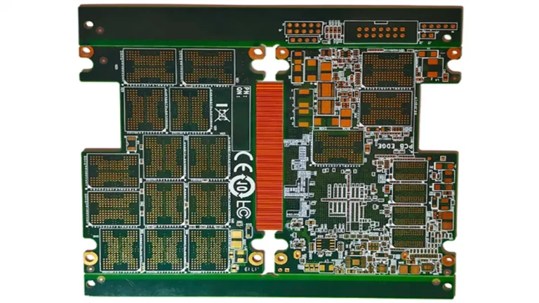
The Importance of HDI PCBs in Multi-Layer Industrial Control Boards
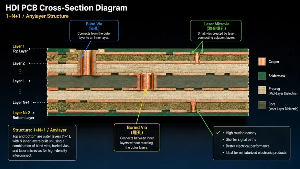
A detailed HDI PCB cross-section diagram showcasing a 1+N+1 anylayer stackup. The integration of laser microvias, blind vias, and buried vias enables shorter signal paths and maximum routing density required for advanced PLC hardware.
HDI technology resolves layout bottlenecks by utilizing microvias, blind vias, and buried vias. This allows designers to route high-pin-count Ball Grid Arrays (BGAs) with finer pitches, routing more traces through fewer layers.
By bringing vias directly into the component pads (via-in-pad technology), HDI significantly shortens signal paths. This structural shift minimizes signal distortion, guarantees robust signal integrity, and cuts down the overall board footprint, making it the perfect architectural fit for multi-layer industrial control systems.
Low-Power Design for Industrial Automation HDI PCBs
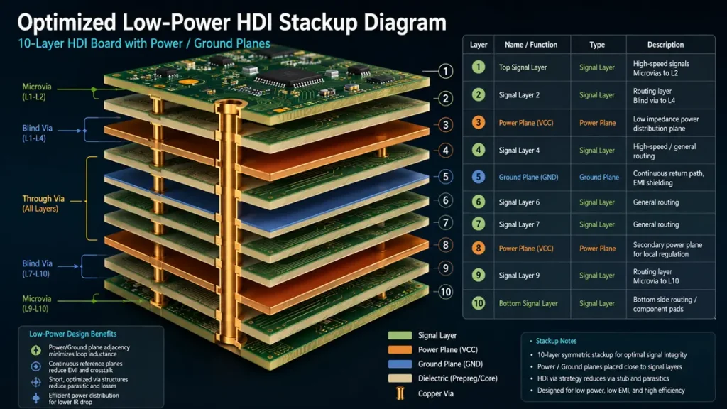
An optimized 10-layer HDI PCB stackup diagram designed for low power consumption and low EMI. Close proximity between power and ground planes significantly minimizes loop inductance, ensuring stable and energy-efficient performance in rugged industrial environments.
With edge computing operating 24/7 in unventilated or sealed industrial enclosures, energy conservation and thermal mitigation are paramount to structural longevity.
Power Optimization Strategies in HDI Stackups
Minimizing power loss begins with strategic layer stackup engineering. By reducing the dielectric thickness between power and ground planes, manufacturers can dramatically boost inter-plane capacitance. This structural optimization dampens power supply noise and stabilizes voltage distribution across high-speed processors, preventing unnecessary power dissipation caused by transient voltage fluctuations.
Selecting Materials for Thermal and Energy Efficiency
Industrial deployment demands base materials that can withstand continuous thermal stress. High-Tg (Glass Transition Temperature) FR4 substrates and low-loss hydrocarbon laminates ensure the PCB maintains structural and electrical stability under high temperatures. Optimized material selection helps limit parasitic dielectric losses ($\tan \delta$), reducing power draw and ensuring that generated heat is effectively dissipated through the board’s internal copper structures rather than pooling beneath crucial processing chips.
Typical Low-Power Stackup Concept:
+------------------------------------------+  Top Signal Layer (Microvia Type I)
|====== Dielectric (Low-Loss/High-Tg) =====|
+==========================================+  Solid Ground Plane (Shielding)
|====== Dielectric ========================|
+==========================================+  Power Plane (Optimized Capacitance)
Case Study: Reducing Power Loss in AI-Driven PLC Modules
In a recent engineering overhaul of an AI-driven PLC module, traditional mechanical via routing was swapped for a 1+N+1 HDI architecture. By moving to via-in-pad microvias, the routing loop area dropped significantly. Coupled with a low-loss, high-Tg substrate, the modification reduced parasitic inductance by over 25% and cut thermal heat dissipation from power delivery networks (PDN) by 14%, allowing the module to run cooler and draw less baseline power in enclosed field conditions.
Scaling Up: Mass Production for Industrial Automation OEMs
Transitioning a complex HDI design from prototype to high-volume manufacturing requires a manufacturing partner with extreme process control and robust logistics.
Delivering Stable Mass Production for Automation OEMs
Industrial OEMs operate on strict timelines where manufacturing downtime is not an option. Mass-producing HDI boards requires consistent, high-precision laser drilling for microvias, alongside automated chemical plating lines to ensure dependable copper filling. Every batch must replicate the exact electrical properties of the approved golden prototype.
Yield Optimization and Defect Control in HDI Manufacturing
The high density of traces in HDI layouts leaves very little margin for error. To optimize yield and eliminate structural defects like trace breakouts or voided vias, premier manufacturers employ strict cross-sectional analysis, statistical process control (SPC), and state-of-the-art automated optical inspection systems. Controlling the chemistry of copper plating baths and laser registration parameters keeps scrap rates low and production lines cost-efficient.
Supply Chain Reliability for Long-Term Industrial Deployments
Industrial control systems often carry a production lifecycle spanning 5 to 10 years. Unlike consumer electronics, components and substrates cannot be phased out arbitrarily. Hardware manufacturers must secure reliable raw material supply chains, ensuring long-term access to identical high-Tg laminates, chemistry options, and copper foils to maintain certification compliance over years of continuous fulfillment.
Strategic Procurement: Annual Contract Sourcing for HDI PCBs
To safeguard against market volatility, forward-thinking procurement teams utilize long-term corporate frameworks to lock in pricing and capacity.
Benefits of an Annual Framework Agreement
Signing an Annual Framework Agreement transforms the traditional transactional vendor relationship into a strategic operational partnership. It guarantees the buyer a dedicated slice of factory production capacity, which shields them from sudden market shortages or seasonal manufacturing crunches.
Cost Control and Long-Term Price Stability
The electronics market is prone to sudden fluctuations in copper prices, laminate availability, and logistics overheads. An annual contract stabilizes per-unit costs, allowing industrial OEMs to forecast yearly expenditures accurately, control their margins, and avoid unexpected price spikes during supply disruptions.
Inventory Planning and Flexible Delivery Scheduling
Rather than storing thousands of completed boards in expensive, unconditioned warehouses, annual contracts allow for rolling inventory schedules. Systems like Just-In-Time (JIT) or Vendor-Managed Inventory (VMI) enable production to happen in balanced batches, with shipments scheduled to arrive precisely when the assembly lines need them.
2026 Breakthroughs: Advanced PCB Manufacturing Technologies
As we progress through the second half of 2026, the boundaries of printed circuit board fabrication are being pushed further by cutting-edge industrial demands.
Ultra-Fine Line and Space via mSAP (Modified Semi-Additive Process)
Traditional subtractive etching reaches its physical limits below 30µm trace widths, often resulting in trapezoidal trace profiles that degrade high-frequency signals. In H2 2026, mSAP (modified Semi-Additive Process) has taken center stage in industrial automation board production. By chemically plating copper onto thin seed layers over flash-etched substrates, mSAP achieves ultra-precise, vertical rectangular trace geometries with line/space dimensions down to 15µm/15µm. This allows for unprecedented routing density inside compact sensor housings.
High-Layer Count HDI Stackups for AI-Integrated Automation
The injection of edge-AI into automation hardware has triggered a dramatic shift toward high-layer count HDI boards. Industrial control systems now utilize complex Anylayer HDI structures scaling up to dozens of layers. These architectures seamlessly interconnect highly complex AI accelerators, multi-core CPUs, and dense memory modules across layers without adding trace lengths that compromise processing latency.
Advanced Materials: Ultra-Low-Loss Laminates and Extreme High-Tg Substrates
With 2026 systems pushing higher data frequencies, standard FR4 materials are quickly becoming obsolete for premium control modules. Next-generation fabrications rely heavily on ultra-low-loss laminates featuring exceptionally low dissipation factors ($D_f \le 0.002$) alongside extreme high-Tg substrates ($\ge \text{180}^\circ\text{C}$). These materials protect the board against structural delamination during multi-stage reflow cycles and keep signal attenuation low over long distances.
Upgraded Automated Optical (AOI) and X-Ray (AXI) Inspection Technologies
As microvias shrink and layer stacks deepen, surface-level visual checks become ineffective. 2026 production lines rely on AI-enhanced 3D Automated Optical Inspection (AOI) alongside real-time Automated X-ray Inspection (AXI). These advanced systems scan inside hidden buried vias and inner-layer traces to flag microscopic flaws, delamination, or minor voiding before the product ever leaves the factory floor.
How Shenzhen Hongda Circuit Technology Co., Ltd. Solves Buyer Pain Points
Navigating the complexities of high-end HDI sourcing requires a manufacturing partner that combines technical excellence with flexible business services. Shenzhen Hongda Circuit Technology Co., Ltd. is purpose-built to address the core challenges faced by hardware engineers and procurement managers in the industrial sector.
- PLC Compatibility and Customization Capabilities: We specialize in translating highly complex engineering requirements into high-performing physical boards. Whether your design demands ultra-dense BGA pitches, specific impedance profiles, or custom multi-layer hybrid stackups, our team delivers custom fabrications engineered explicitly for industrial PLC and automation workloads.
- Low-Power Design Engineering Support: Our engineering experts provide comprehensive DFM (Design for Manufacturing) feedback before production starts. We review your layer stackup, advice on via configurations, and help select optimal high-Tg, low-loss materials to minimize power dissipation and maximize thermal efficiency under harsh operating conditions.
- High-Volume Production with Consistent Quality: Operating state-of-the-art automated fabrication lines, we seamlessly scale projects from initial engineering prototypes up to high-volume mass production. Our stringent quality controls ensure that every batch meets the same rigorous structural and electrical standards required for long-term industrial deployments.
- Rapid Quoting and Engineering Feedback Cycles: In the fast-paced electronics market, waiting weeks for a quote stalls development. We offer rapid quoting turnarounds combined with deep engineering reviews, identifying potential manufacturability issues early to shave weeks off your product launch window.
- Exclusive Support for Annual Contract Partners: For customers looking for stable pricing and volume guarantees, we offer dedicated annual framework agreements. We provide locked-in contract pricing, priority manufacturing queue allocation, and customized rolling delivery schedules to align with your production requirements throughout the year.
For inquiries or to submit a design file for a technical review, contact our engineering team directly at sales@pcbkr.com.
Technical & Procurement FAQ (Supplier Evaluation Guide)
What is your factory’s monthly production capacity for high-layer count HDI PCBs?
Our facility is fully equipped for scaling up industrial needs, featuring a monthly production capacity exceeding 50,000 square meters of high-precision printed circuit boards. This includes dedicated production lanes optimized for multi-layer HDI fabrications, allowing us to seamlessly manage both fast-turn prototyping runs and large-scale mass production for global OEMs.
Can you provide long-term annual contracts with locked-in pricing and stable delivery timelines?
Yes. We offer Annual Framework Agreements specifically designed for industrial procurement teams. Under these contracts, we lock in your per-unit pricing against market fluctuations for 12 months, reserve a dedicated portion of our manufacturing capacity for your orders, and support flexible delivery schedules (such as JIT or quarterly releases) to match your manufacturing forecasts.
Which testing and reliability standards do your industrial automation PCBs comply with?
All our industrial automation boards are manufactured and inspected under strict global standards, including IPC-A-600 Class 2 and Class 3 compliance. To ensure survivability in rugged field deployments, our quality control process includes:
Automated X-Ray Inspection (AXI) and 3D AOI testing.
Thermal Shock and Thermal Cycling testing to prevent field delamination.
Controlled Impedance Testing with full reporting.
Solderability testing, Micro-section analysis, and IST (Interconnect Stress Testing) upon request.
How do your manufacturing processes help ensure low power consumption and thermal stability in HDI PCBs?
We control power loss by utilizing precision laser drilling and advanced copper-filling techniques that minimize parasitic resistance and loop inductance in your Power Delivery Network (PDN). Additionally, we work closely with leading material vendors to source ultra-low-loss laminates (Df) and high-thermal-conductivity substrates, ensuring minimal energy loss and efficient heat transfer away from active processing components.
Find Out About Us: Delivering Top-Tier Fabrication for Both AI & Conventional PCBs
Navigating the line between cutting-edge innovation and high-volume, cost-effective production shouldn’t be a compromise. At Shenzhen Hongda Circuit Technology (PCBKR), we bridge this gap by elevating the manufacturing standards for both high-performance AI hardware and traditional multi-layer PCBs.
By integrating advanced manufacturing methodologies across all production lines, we bring an elite level of precision to traditional PCB fabrication. Our standard boards benefit from enhanced interlayer alignment tolerances (down from ±75μm to within ±25μm) and tightened differential impedance control (±5%). Supported by 100% 3D X-Ray (AXI) inspection, your conventional boards achieve chip-level reliability, superb signal stability, and near-100% yield.
Your Strategic Manufacturing Partner
We proudly stand as a dual-capability partner: offering the elite technical ceiling required for next-gen AI hardware, while maintaining the exceptional flexibility, rapid turnaround, and unmatched cost-efficiency needed for mid-to-high-volume traditional board campaigns. You get zero-defect reliability without the premium overhead or bureaucracy of massive tier-1 factories.
Ready to upgrade your hardware’s reliability?
Submit your Gerber files today for an agile engineering review and a highly competitive quote.
Contact our experts: sales@pcbkr.com
About Author
David Chen https://www.linkedin.com/in/pcbcoming
David Chen boasts an extensive professional background in PCBA manufacturing, PCBA testing, and PCBA optimization, with specialized expertise in high-precision PCBA fault analysis and rigorous PCBA reliability testing. The author has worked with high-layer-count server PCB fabrication, ultra-low-loss backplane stackups, and thermo-mechanical reliability optimization for AI infrastructure projects involving 112G and 224G PAM4 architectures. Skilled in complex circuit design and cutting-edge advanced PCB manufacturing processes, he delivers solutions that elevate product durability and performance across industrial applications. His technical articles focusing on PCBA manufacturing workflows and testing methodologies are widely cited by industry peers, research institutions, and technical platforms, solidifying his reputation as a recognized technical authority in the global circuit board manufacturing sector.