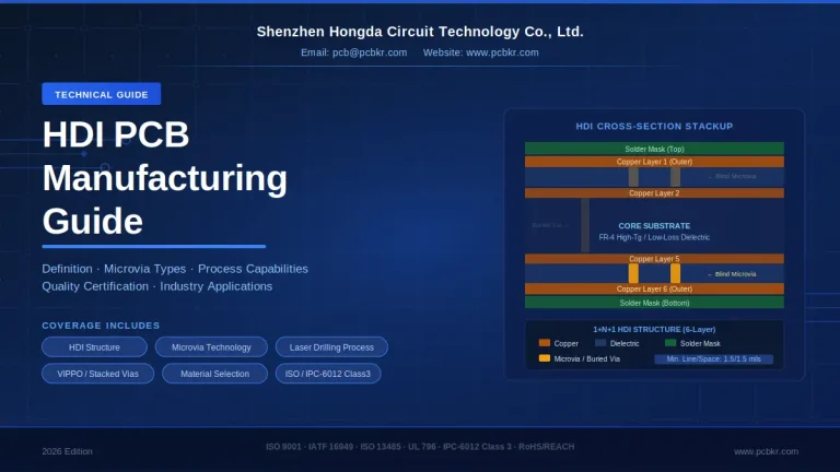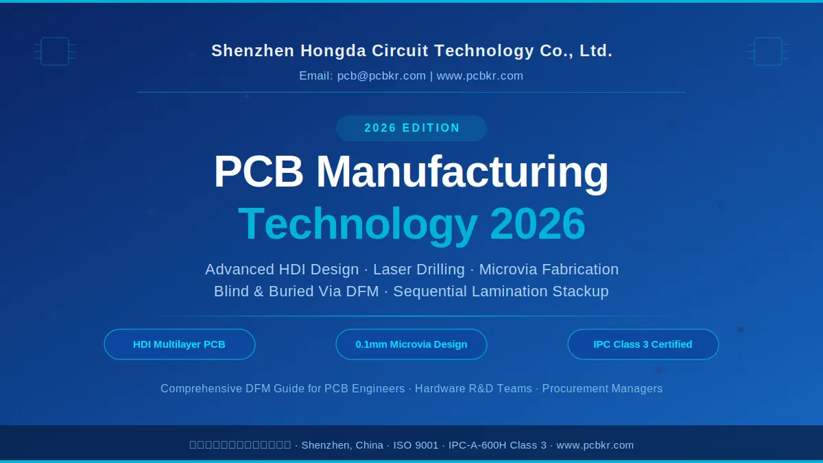
Advanced HDI Design, Laser Drilling & High-Density Fabrication Guide
Summary: This comprehensive guide covers 2026 PCB manufacturing technology, including HDI multilayer PCB design, microvia fabrication, laser drilling process, blind and buried via DFM rules, and lamination stackup strategies. Designed for PCB layout engineers, hardware R&D teams, and procurement managers seeking a certified high-density interconnect manufacturer in Shenzhen.
The 2026 PCB Manufacturing Landscape: Why HDI Technology Defines the Next Generation
The global printed circuit board industry is undergoing its most significant transformation in two decades. Driven by the explosive growth of AI servers, 5G base stations, automotive ADAS systems, and advanced consumer electronics, PCB manufacturing technology in 2026 demands unprecedented levels of density, signal integrity, and reliability. High-Density Interconnect (HDI) PCB design has shifted from a specialty process to a mainstream requirement.
At Shenzhen Hongda Circuit Technology Co., Ltd., we have observed a clear market inflection point: customers who previously specified standard multilayer PCB fabrication are now requesting HDI board manufacturing with 0.1mm microvia structures, laser-drilled blind vias, and sequential lamination stackups. This guide consolidates our engineering expertise to help you understand and implement modern PCB manufacturing standards.
1. Key PCB Technology Trends Shaping 2026 Manufacturing Demands
- AI accelerator boards require 16+ layer HDI PCB stackups with sub-100 micron via structures
- High-speed PCB design at 112 Gbps PAM4 signals demands controlled-impedance HDI routing
- Advanced packaging (chiplets, 2.5D/3D IC) drives need for ultra-fine pitch BGA escape routing via microvias
- Automotive PCB manufacturing standards (IPC-6012DA) now mandate HDI reliability testing
- Medical device PCBs increasingly require HDI miniaturization without sacrificing electrical performance
What Is HDI PCB Technology? Definitions, Structures, and 2026 Design Standards
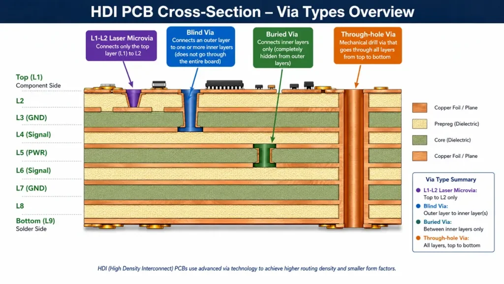
Cross-sectional view of a high-density interconnect (HDI) multilayer PCB stackup, illustrating the physical structural differences between laser-drilled microvias, blind vias, buried vias, and standard mechanical through-holes.
High-Density Interconnect (HDI) PCB technology is defined by IPC-2226 as a printed circuit board with a higher wiring density per unit area than conventional PCBs. The defining characteristic of HDI board manufacturing is the use of microvias — vias with a finished hole diameter of 0.15 mm or less — fabricated using laser drilling rather than mechanical drilling.
1. HDI PCB Design: Core Structural Elements
Modern HDI multilayer PCB design incorporates three fundamental interconnect types that distinguish it from standard through-hole technology:
| Via Type | Definition | Layer Connection | Drill Method | Min. Diameter (2026 Standard) |
| Microvia | Blind via with depth ≤ 1× diameter | L1 to L2 (surface to adjacent) | CO2 / UV Laser | 0.075 mm |
| Blind Via | Via connecting outer to inner layer, not penetrating full board | e.g., L1–L3, L1–L4 | Laser or Controlled Depth | 0.10 mm |
| Buried Via | Via entirely within inner layers, invisible from surface | e.g., L3–L4, L4–L5 | Mechanical drill (pre-lamination) | 0.15 mm |
| Through-hole Via | Full-stack via from top to bottom | L1 to Ln | CNC Mechanical Drill | 0.20 mm |
2. HDI PCB Advantages Over Conventional Multilayer Boards
- Routing density increase of 40–70% compared to standard multilayer PCB fabrication
- Reduction in PCB layer count while maintaining equivalent connectivity — significant cost optimization
- Improved signal integrity due to shorter via stubs and reduced parasitic inductance
- Smaller finished board size — critical for wearables, IoT modules, and mobile devices
- Enhanced thermal management through optimized copper distribution and via-in-pad structures
Laser Drilling Technology in HDI PCB Manufacturing: 2026 Process Capabilities
Laser drilling is the enabling technology behind HDI PCB manufacturing. Unlike mechanical CNC drilling, which is limited by drill bit physics to approximately 0.20 mm minimum diameter, laser drilling uses focused photonic energy to ablate material with precision down to 0.050 mm in advanced configurations. Shenzhen Hongda Circuit Technology operates both CO2 infrared lasers and UV (355 nm) solid-state lasers to serve the full spectrum of HDI manufacturing requirements.
1. Laser Drilling Process for Microvia PCB Fabrication
The laser drilling sequence in HDI circuit board manufacturing follows a defined process flow:
- Surface preparation: Copper foil on the target layer is chemically treated or pre-drilled to define drill target geometry
- CO2 laser ablation: The dielectric (FR4, Rogers, or specialty substrate) is ablated by the infrared laser beam in a single or multi-pulse sequence
- UV laser conformal drilling: For finer features or copper direct drilling, UV laser provides tighter beam focus and reduced heat-affected zone
- Desmear and electroless copper: Laser-drilled via walls are cleaned and metallized to establish electrical continuity
- Panel plating: Copper electroplating fills or partially fills the microvia to achieve target hole copper thickness
2. Laser Drilling vs. Mechanical Drilling: PCB Manufacturing Comparison
| Parameter | Laser Drilling (HDI) | Mechanical Drilling (Standard PCB) |
| Minimum diameter | 0.075–0.10 mm standard; 0.050 mm advanced | 0.20 mm production; 0.15 mm premium |
| Aspect ratio limit | 0.8:1 (depth:diameter) | 10:1 typical |
| Positional accuracy | ±0.025 mm (laser) | ±0.05 mm |
| Applicable layers | Surface layers only (blind/microvia) | All layers (through-hole) |
| Cost driver | Machine time per via | Drill bit wear and change |
| Best for | HDI, BGA fanout, high-density routing | Power vias, connectors, standard PCBs |
3. Laser Drilling Design Rules: What PCB Engineers Must Know in 2026
To achieve maximum yield in HDI PCB fabrication, designers must adhere to laser drilling constraints that Shenzhen Hongda Circuit Technology has validated across thousands of production panels:
- Minimum microvia diameter: 0.10 mm standard production; 0.075 mm in advanced HDI process
- Maximum aspect ratio: 1:1 (depth equals diameter). A 0.10 mm laser-drilled via must not penetrate more than 0.10 mm of dielectric
- Pad diameter for 0.10 mm microvia: minimum 0.25 mm finished pad to ensure adequate annular ring
- Minimum annular ring: 0.05 mm after drill registration tolerance is accounted for
- Via-to-trace clearance: minimum 0.075 mm from microvia pad edge to nearest copper feature
- Copper foil thickness on target layer: recommend 0.5 oz (17 micron) for optimal CO2 laser ablation stop
| Design Warning: Specifying a 0.10 mm microvia with insufficient pad size (< 0.20 mm) is one of the most common HDI DFM failures. When laser beam registration error is applied, the annular ring collapses, causing open circuits after reliability testing. Always add pad with a minimum 0.075 mm annular ring beyond the finished hole size. |
0.1mm Microvia Design DFM Rules: Achieving High-Yield HDI PCB Manufacturing
The 0.1 mm microvia (100-micron diameter) represents the workhorse structure in modern HDI multilayer PCB manufacturing. At this scale, the margin between a manufacturable design and a yield-killing layout narrows considerably. DFM (Design for Manufacturability) compliance at the microvia level directly determines production yield, reliability test pass rates, and long-term field performance.
1. Microvia Pad-to-Hole Ratio Requirements for HDI Fabrication
The pad-to-hole ratio is the single most critical geometric parameter in 0.1 mm microvia design. This ratio determines the annular ring width available after laser drilling registration error and etching tolerances are applied:
| Microvia Diameter | Recommended Pad Diameter | Minimum Pad Diameter | Annular Ring (Nominal) | Risk Level |
| 0.075 mm | 0.225 mm | 0.175 mm | 0.075 mm | High — advanced process only |
| 0.10 mm | 0.275 mm | 0.225 mm | 0.0875 mm | Medium — standard HDI |
| 0.125 mm | 0.325 mm | 0.275 mm | 0.10 mm | Low — preferred for new designs |
| 0.15 mm | 0.35 mm | 0.30 mm | 0.10 mm | Very Low — conservative HDI |
2. Aspect Ratio Control in HDI Microvia Manufacturing
The aspect ratio (AR) of a laser-drilled microvia is defined as the ratio of via depth to via diameter. Exceeding the process-validated aspect ratio leads to incomplete copper plating inside the via barrel, creating voids, reduced mechanical strength, and eventual open-circuit failure under thermal cycling:
- AR ≤ 0.8:1 — optimal for high-reliability HDI PCB manufacturing (recommended by IPC-2226)
- AR 0.8:1 to 1.0:1 — acceptable with enhanced plating chemistry; requires tighter process control
- AR > 1.0:1 — not recommended; high risk of plating void and reliability failure
For a standard 0.10 mm microvia, maximum via depth should not exceed 0.08–0.10 mm. This limits the dielectric layer thickness between laminated layers in the HDI stackup — an important constraint when planning 1+N+1 or 2+N+2 HDI structures.
3. Via-in-Pad (VIP) and Stacked Microvia Considerations
Via-in-pad (VIP) structures, where the microvia is placed directly beneath a BGA or component pad, are increasingly common in 2026 high-density PCB designs. Key manufacturing requirements include:
- Microvia must be copper-filled (not just plated through) before surface finish application to prevent solder void formation during reflow
- Fill height tolerance: copper fill must be within 0.015 mm of flush with the surrounding copper plane
- Stacked microvia (microvia atop microvia across multiple HDI build-up layers) requires sequential lamination and carries higher misregistration risk — validated capability at Hongda: ±0.025 mm layer-to-layer registration
- Staggered microvia (offset horizontally on adjacent layers) is preferred over stacked via for yield optimization in volume HDI PCB production
Blind and Buried Via DFM Rules for Advanced Multilayer PCB Design
While microvias handle surface-layer high-density interconnects, blind vias and buried vias extend the HDI routing paradigm into the inner layer structure of complex multilayer PCBs. Understanding the manufacturing constraints of each interconnect type is essential for cost-effective PCB design.
1. Blind Via Design Rules for HDI Circuit Board Manufacturing
A blind via connects an external layer to one or more internal layers without penetrating the entire board. In HDI PCB manufacturing, blind vias are typically formed by laser drilling in the build-up layers or by controlled-depth mechanical drilling in the core layers:
- Minimum blind via diameter: 0.10 mm (laser); 0.20 mm (mechanical controlled-depth)
- Blind via must not skip more than 2 adjacent copper layers — deeper blind vias exceed laser aspect ratio limits
- Blind via pad on buried layer must have full copper annular ring; partial pad designs cause drilling registration failures
- Blind via to blind via clearance: minimum 0.15 mm pad edge to pad edge
- Adjacent blind vias on opposing sides of the board (from L1–L2 and from Ln–Ln-1) must be offset horizontally by ≥ 1 pad diameter to prevent dielectric cracking during lamination
2. Buried Via Design Constraints in Sequential Lamination PCBs
Buried vias exist entirely within the inner layers and are fabricated before the outer layer build-up process begins. This makes buried vias the most cost-impactful via type in multilayer PCB manufacturing, as they require a separate drilling and plating step on the sub-composite before final lamination:
- Minimum buried via diameter: 0.15 mm (laser-assisted); 0.20 mm (mechanical drill on sub-composite)
- Buried via must be fully copper-filled or plugged before additional lamination; any void in the buried via creates a pressure concentration point during subsequent hot-press cycles
- Buried via location must account for post-lamination layer shift; maintain 0.10 mm additional pad margin beyond standard DFM requirements
- Buried vias between non-adjacent inner layers (e.g., L4–L6 in a 10-layer PCB) require a sub-composite press cycle, increasing manufacturing cost and lead time
3. Via Type Selection Guide for Cost-Optimized HDI PCB Design
| Design Scenario | Recommended Via Type | Cost Index | Manufacturing Complexity |
| BGA fanout < 0.80 mm pitch | Microvia (0.10 mm laser) | Medium | High |
| General signal routing, inner layers | Through-hole via (0.20 mm) | Low | Low |
| Component density < 500 mm² | Standard multilayer, no HDI | Lowest | Lowest |
| High-speed differential pair escape | Blind via (L1–L2 laser) | Medium | Medium |
| Power and GND plane connection, inner layers | Buried via (L3–L6) | High | High |
| Ultra-fine pitch (< 0.65 mm) BGA in 2026 designs | Stacked microvia VIP | Highest | Very High |
HDI PCB Stackup Design: 1+N+1 and 2+N+2 Structures Explained
The HDI stackup nomenclature — 1+N+1, 2+N+2, 3+N+3 — describes the number of sequential build-up layers applied to each side of the core multilayer PCB (N). Understanding stackup selection is critical for balancing routing density, manufacturing yield, and fabrication cost in 2026 HDI PCB projects.
1. 1+N+1 HDI PCB Stackup: Single Build-Up Layer Structure
The 1+N+1 HDI stackup is the most common and cost-efficient HDI configuration. It consists of one laser-drilled build-up layer on each side of the conventional multilayer core (N layers):
- Typical configuration: L1 (build-up) + core (L2–Ln-1) + Ln (build-up)
- Microvias exist only between L1–L2 and Ln–Ln-1
- All inner-layer routing uses through-hole or buried vias in the core
- One lamination cycle for core + one co-lamination cycle for build-up layers = 2 total press cycles
- Cost advantage: 15–25% lower than 2+N+2 for equivalent layer count
- Suitable for: mid-range smartphones, industrial controllers, networking switches, LED driver boards
| Hongda Capability (1+N+1): Shenzhen Hongda Circuit Technology supports 1+N+1 HDI boards up to 20 total layers with 0.10 mm laser microvias, ±0.025 mm registration accuracy, and IPC Class 3 reliability standards. |
2. 2+N+2 HDI PCB Stackup: Dual Build-Up Layer Structure
The 2+N+2 stackup adds a second build-up layer to each side of the core, enabling two tiers of laser microvias. This is the standard architecture for high-end smartphones, AI inference modules, server daughtercards, and advanced automotive ECUs in 2026:
- Configuration: L1 (build-up 2) + L2 (build-up 1) + core (L3–Ln-2) + Ln-1 (build-up 1) + Ln (build-up 2)
- Microvias exist on L1–L2, L2–L3, Ln-1–Ln, and Ln-2–Ln-1
- Stacked microvias (L1 via stacked on L2 via) are possible but add registration risk
- Requires 3 sequential lamination cycles: core press, first build-up press, second build-up press
- Routing density increase: 60–90% over equivalent 1+N+1 for sub-0.8 mm pitch BGA designs
- Cost premium: 30–50% over 1+N+1 due to additional lamination and laser drilling cycles
For standard controlled-impedance stackup configurations beyond HDI structures, please refer to our comprehensive [Ultimate Guide to Multilayer PCB Stackup Design
3. Advanced HDI Stackups: 3+N+3 and Any-Layer HDI
For leading-edge PCB applications in 2026 — including AI GPU carrier boards, high-bandwidth memory (HBM) interfaces, and high-frequency RF substrates — three or more build-up layers may be required. Any-layer HDI, where every layer is a build-up layer and any-to-any layer connection is achievable via stacked microvias, represents the state of the art in HDI multilayer PCB manufacturing. Shenzhen Hongda Circuit Technology provides engineering consultation for any-layer HDI feasibility assessment upon request.
Sequential Lamination Process in HDI PCB Manufacturing: DFM Constraints and Yield Optimization
Sequential lamination is the manufacturing process that makes HDI PCB structures physically possible. Unlike conventional multilayer PCB fabrication — where all layers are laminated in a single press cycle — HDI boards require multiple sequential press cycles to build up the laser-drilled interconnect layers incrementally. Each sequential lamination cycle introduces compounding alignment tolerances and material stress risks that PCB designers must account for during layout.
1. Sequential Lamination Process Flow for 2+N+2 HDI PCB
- Step 1 — Core fabrication: Inner layer imaging, etching, and inspection of N-layer core. Through-hole via drilling and plating for core layer interconnects.
- Step 2 — First build-up lamination: Prepreg and copper foil are applied to both sides of the core under controlled temperature (180–200°C) and pressure. CO2 laser drilling of first-tier microvias (L2–L3 and Ln-2–Ln-1).
- Step 3 — First build-up plating and imaging: Electroless and electrolytic copper plating of first-tier vias. Photolithographic imaging and etching of L2 and Ln-1 copper traces.
- Step 4 — Second build-up lamination: Second prepreg and copper foil layer laminated onto first build-up surface. Laser drilling of second-tier microvias (L1–L2 and Ln–Ln-1).
- Step 5 — Final plating, imaging, and finishing: Full panel copper plating, outer layer imaging, solder mask, surface finish (ENIG, ENEPIG, or OSP), electrical test, and final inspection.
2. Layer Registration Accuracy in Sequential Lamination HDI Manufacturing
Each sequential lamination cycle introduces cumulative X-Y registration error between the newly laminated copper layer and the underlying drilled via targets. At Shenzhen Hongda Circuit Technology, our advanced lamination equipment achieves the following registration performance:
| HDI Stackup Level | Layer-to-Layer Registration (3σ) | Impact on Microvia Annular Ring | Recommended Pad Margin |
| 1+N+1 (1st build-up) | ±0.025 mm | Negligible with 0.075 mm annular ring target | +0.025 mm beyond minimum |
| 2+N+2 (2nd build-up) | ±0.040 mm | Moderate — annular ring may reduce 30% | +0.040 mm beyond minimum |
| 3+N+3 (3rd build-up) | ±0.060 mm | Significant — requires reinforced pad design | +0.075 mm beyond minimum |
| Any-layer HDI | ±0.080 mm | Critical — stacked via offset mandatory | +0.100 mm beyond minimum |
3. Material Selection Considerations for HDI Sequential Lamination
The dielectric material used in HDI build-up layers critically affects laser drilling quality, thermal reliability, and signal performance. For 2026 HDI PCB manufacturing, the following materials are commonly specified:
- Standard FR4 (Tg 150–170°C): Suitable for general HDI applications; laser drilling requires window opening due to glass fiber content
- High-speed FR4 (Tg 170°C+, Dk 3.5–3.8): Preferred for HDI boards with differential pairs above 10 Gbps; reduced dielectric loss versus standard FR4
- PTFE-based laminates (Rogers RO4000 series, Dk 3.38–3.55): Used in RF/microwave HDI boards; laser drilling requires UV laser for clean via walls
- BT (Bismaleimide Triazine) resin build-up film: High Tg (190°C+), excellent dimensional stability; common in IC package substrate HDI manufacturing
- Megtron 6 / IS680A: Ultra-low-loss dielectric for PCIe 6.0, 800G Ethernet, and AI server HDI applications in 2026
Best Practices for High-Yield HDI PCB Design: Engineering Recommendations from Hongda
After manufacturing over 50,000 HDI PCB panel variants since our founding, Shenzhen Hongda Circuit Technology has compiled the following engineering best practices for designers targeting high-yield, high-reliability HDI multilayer PCB production in 2026. These recommendations are derived from our internal DFM analysis database and align with IPC-2226 Class C HDI design standards.
1. Microvia Size and Aspect Ratio — Getting the Foundation Right
- Default to 0.10 mm microvias over 0.075 mm unless BGA pitch absolutely demands it — yield loss at 0.075 mm is 3–5× higher than at 0.10 mm in standard production volumes
- Check dielectric thickness against microvia diameter before finalizing stackup — common mistake is selecting a build-up prepreg (e.g., 0.10 mm thick) that creates a 1:1 aspect ratio at 0.10 mm via size
- For copper-filled VIP structures, add 0.015 mm to the nominal microvia copper fill spec when ordering to account for polishing tolerance
- Do not mix laser microvias and mechanical vias on the same BGA fanout area — differential drill accuracy causes pad-to-drill misalignment
2. Stacked vs. Staggered Microvia Strategy for 2+N+2 Designs
The choice between stacked and staggered microvias in 2+N+2 HDI designs is one of the most impactful yield decisions a PCB designer makes:
- Stacked microvias (L1 via directly atop L2 via): Requires precise copper fill of first-tier via before second lamination; void in L2 via propagates stress to L1 via during thermal cycling; maximum yield at Hongda production scale with copper fill guaranteed
- Staggered microvias (L1 via offset 0.05–0.10 mm from L2 via): Higher routing flexibility; eliminates stacked-via interface reliability risk; preferred architecture for IPC Class 3 reliability requirements
- For high-reliability applications (aerospace, medical, automotive ADAS): Always specify staggered microvias and IPC Class 3 acceptance criteria
3. DFM Checklist for HDI PCB Design Submission to Hongda
- Confirm microvia diameter, pad diameter, and annular ring for every build-up layer in the stackup
- Verify all via aspect ratios against the dielectric thickness in the selected prepreg
- Specify via fill requirements explicitly: copper fill, resin plug, or no fill — do not leave this as a manufacturer default
- Include via-in-pad locations in a separate callout on the fabrication drawing
- Define sequential lamination stackup as a numbered layer table with dielectric thickness, copper weight, and material designation
- Identify any stacked microvia locations and specify fill process for sub-via
- Provide impedance control requirements with reference stack layer, trace width, and target impedance value
- Flag any blind vias deeper than L1–L3 or Ln–Ln-2 for DFM review before release
Shenzhen Hongda Circuit Technology: HDI PCB Manufacturing Capabilities and Certifications
Shenzhen Hongda Circuit Technology Co., Ltd. is an IPC-certified PCB manufacturer specializing in high-density interconnect (HDI) multilayer PCB fabrication. Located in Shenzhen — the global center of advanced electronics manufacturing — Hongda provides end-to-end PCB manufacturing services from prototype through high-volume production.
1. Core HDI PCB Manufacturing Specifications
| Capability Parameter | Hongda Standard | Hongda Advanced | Industry Benchmark 2026 |
| Minimum microvia diameter | 0.10 mm | 0.075 mm | 0.050 mm (R&D) |
| Laser type | CO2 (infrared) | CO2 + UV combo | UV / excimer |
| Layer count (HDI) | 2–16 layers | 16–24 layers | Up to 40 layers |
| Max stackup | 1+N+1 | 2+N+2 | Any-layer HDI |
| Layer registration (3σ) | ±0.040 mm | ±0.025 mm | ±0.015 mm (R&D) |
| Surface finish options | HASL, ENIG, OSP | + ENEPIG, Hard Gold | + Immersion Tin/Silver |
| Min trace/space | 0.075/0.075 mm | 0.050/0.050 mm | 0.025/0.025 mm |
| Controlled impedance tolerance | ±10% | ±5% | ±3% |
| Certifications | ISO 9001, IPC-A-600 | ISO 9001, IPC-A-600, UL | IATF 16949 (automotive) |
2. DFM Engineering Support — Design Collaboration Before Fabrication
One of Shenzhen Hongda Circuit Technology’s key differentiators in the HDI PCB market is our pre-production DFM (Design for Manufacturability) review service. Before any HDI board enters the production queue, our engineering team reviews:
- Microvia geometry vs. laser drilling capability — pad diameter, annular ring, and aspect ratio verification
- Stackup feasibility — dielectric thickness compatibility with via depth requirements
- Sequential lamination sequence — layer build order, lamination cycle count, and material compatibility
- Via fill specification — copper fill vs. resin plug selection based on downstream assembly requirements
- Impedance stack modeling — simulated differential and single-ended impedance vs. customer targets
- BGA fanout analysis — escape routing density assessment and via placement optimization
DFM feedback is provided within 24 hours for standard HDI boards and 48 hours for complex any-layer HDI or RF/microwave substrate designs.
3. Quality Assurance in HDI PCB Production at Hongda
- 100% electrical test (flying probe or fixture-based) on all HDI boards to IPC-ET-652 standards
- AOI (Automated Optical Inspection) on inner and outer layers after each imaging step
- X-ray inspection of copper-filled vias and BGA pad structures for void detection
- Microsection analysis on sample coupons per IPC-A-600H Class 3 acceptance criteria
- Reliability testing available: IST (Interconnect Stress Test), thermal cycling, and ionic contamination
Frequently Asked Questions: HDI PCB Manufacturing in 2026
What is the minimum microvia size Shenzhen Hongda can manufacture in 2026?
Our standard production process supports 0.10 mm (100 micron) finished microvia diameter with CO2 laser drilling. Our advanced process capability reaches 0.075 mm using UV laser drilling, available for volume orders with engineering review. For R&D prototype quantities below 50 panels, 0.075 mm microvias are available with a 3–5 business day engineering consultation lead time.
What is the difference between a 1+N+1 and 2+N+2 HDI stackup, and which should I choose?
A 1+N+1 HDI stackup has one laser-drilled build-up layer on each side of the conventional multilayer core; 2+N+2 has two. Choose 1+N+1 if your BGA pitch is 0.80 mm or larger and your component density is moderate. Choose 2+N+2 if you have sub-0.65 mm BGA components, ultra-high routing density (> 50 nets per cm²), or AI/high-speed signal interfaces at 56 Gbps PAM4 and above. Hongda’s engineering team provides free stackup consultation for customers with BOM and board outline data.
How does laser drilling affect my PCB signal integrity design?
Laser microvias have significantly lower stub length and parasitic capacitance compared to through-hole vias, making HDI boards superior for high-speed PCB design. A 0.10 mm microvia on a 0.10 mm dielectric presents approximately 0.02–0.05 pF capacitance at the via, compared to 0.3–0.8 pF for a standard through-hole via on a 1.6 mm FR4 board. This 10–15× reduction in via capacitance directly improves eye diagram opening at data rates above 25 Gbps.
What certifications does Hongda hold for HDI PCB manufacturing?
Shenzhen Hongda Circuit Technology holds ISO 9001:2015 quality management certification and manufactures to IPC-A-600H Class 2 and Class 3 acceptability standards. Our HDI products comply with RoHS Directive 2011/65/EU (updated 2023 annex) and are UL-recognized for flammability. Automotive HDI boards are produced under an IATF 16949-aligned quality plan; full IATF 16949 certification is available upon customer audit. Please contact our engineering team for certification documentation.
What is the typical lead time for HDI PCB prototype and volume production?
Standard 1+N+1 HDI prototypes (1–10 panels): 5–7 business days. Standard 2+N+2 HDI prototypes: 8–12 business days. Volume production (100+ panels, 1+N+1): 15–20 business days. Volume production (100+ panels, 2+N+2): 20–28 business days. Express services with 3-day and 5-day turnaround are available for 1+N+1 HDI designs meeting standard DFM criteria. Lead times are confirmed at order acceptance following DFM review.
Building the Future with Advanced HDI PCB Manufacturing Technology
As PCB technology enters 2026, the boundary between PCB manufacturing and semiconductor packaging continues to blur. HDI multilayer PCB design — with its laser-drilled microvias, sequential lamination stackups, and sub-0.1 mm feature geometry — is no longer an exotic capability reserved for flagship consumer devices. It is the baseline expectation for any product competing in AI computing, 5G infrastructure, advanced automotive electronics, or next-generation medical devices.
The DFM rules, process parameters, and design guidelines presented in this document represent the current state of practice at Shenzhen Hongda Circuit Technology and align with IPC-2226 and IPC-6016 standards as updated through 2026. Designers who internalize these constraints early in the layout process — before the first Gerber is exported — will experience dramatically higher first-pass yield, shorter revision cycles, and better long-term field reliability.
Shenzhen Hongda Circuit Technology Co., Ltd. invites engineers and procurement teams to engage our technical team for project-specific DFM review, stackup consultation, and HDI PCB manufacturing quotation. Our combination of advanced laser drilling capability, sequential lamination expertise, and rigorous quality management positions us as a trusted manufacturing partner for the most demanding HDI PCB applications globally.
Shenzhen Hongda Circuit Technology Co., Ltd.
Specialized HDI PCB Manufacturer | Shenzhen, China | ISO 9001 | IPC Class 3 Certified
Keywords: HDI PCB manufacturer, microvia PCB design, laser drilling PCB, multilayer PCB fabrication, blind via buried via, 2026 PCB technology, Shenzhen PCB factory
About Author
David Chen https://www.linkedin.com/in/pcbcoming
David Chen boasts an extensive professional background in PCBA manufacturing, PCBA testing, and PCBA optimization, with specialized expertise in high-precision PCBA fault analysis and rigorous PCBA reliability testing. The author has worked with high-layer-count server PCB fabrication, ultra-low-loss backplane stackups, and thermo-mechanical reliability optimization for AI infrastructure projects involving 112G and 224G PAM4 architectures. Skilled in complex circuit design and cutting-edge advanced PCB manufacturing processes, he delivers solutions that elevate product durability and performance across industrial applications. His technical articles focusing on PCBA manufacturing workflows and testing methodologies are widely cited by industry peers, research institutions, and technical platforms, solidifying his reputation as a recognized technical authority in the global circuit board manufacturing sector.