Hybrid Stackup PCB: Why FR4 + Rogers Mixed-Material Construction Delivers the Best Signal Integrity at Scale in 2026
As 112G and 224G PAM4 interconnects become standard across AI servers, data center switches, and high-speed backplanes, PCB designers face a fundamental materials dilemma: full-Rogers constructions deliver clean signal channels but at prohibitive cost, while all-FR4 boards buckle under the insertion loss demands of SerDes at these data rates. Hybrid stackup PCB technology resolves that conflict by placing low-loss dielectric only where the signal physics demand it. This article explains the engineering rationale, manufacturing requirements, and supplier selection criteria engineers and procurement teams need to make confident hybrid layer PCB decisions in 2026.
1. Why 112G/224G High-Speed PCB Design Forces a Materials Rethink
The transition from 25G NRZ to 112G PAM4, and now to 224G PAM4/PAM8, does not simply compress more bits into the same signal bandwidth — it fundamentally changes how a PCB dielectric behaves as a transmission medium. At 56 GHz Nyquist frequencies and beyond, the dielectric loss factor (Df) of standard FR4 laminates, typically between 0.020 and 0.025, begins to dominate the channel loss budget in ways that cannot be corrected by equalization alone.
Signal Integrity Bottlenecks in Conventional FR4 PCB Construction
Standard FR4 was engineered in the 1960s for digital circuits operating well below 1 GHz. Its glass-weave reinforcement introduces Dk variations across the board plane — a phenomenon called fiber-weave effect — that causes differential skew and mode conversion at high data rates. When a 112G SerDes channel must maintain an insertion loss of less than 28 dB across a 400 mm trace, the Df of the laminate at 28 GHz becomes a hard constraint rather than a footnote.
- FR4 Df at 10 GHz typically ranges from 0.018 to 0.025, rising with frequency
- Insertion loss on a 12-inch FR4 trace at 56 GHz (112G Nyquist) can exceed 35 dB, far above the 28 dB budget most SerDes PHYs tolerate
- Jitter accumulation from fiber-weave skew becomes a primary BER limiter above 50 Gbps per lane
- Return loss compliance to OIF-CEI-112G-VSR spec demands dielectric consistency that FR4 cannot guarantee at production scale
The Cost Ceiling on Full High-Frequency Laminate PCB Boards
High-performance laminates such as Rogers 4350B, Megtron 6, or Panasonic Megtron 7 reduce Df to below 0.004 and deliver a far more stable Dk profile across the operating frequency range. The engineering case for these materials is clear. The economic case, particularly for production volumes in AI infrastructure buildouts, is not.
Cost Reference: A 16-layer fully Rogers RO4350B PCB can run 6 to 9 times the laminate cost of an equivalent all-FR4 construction. For a 48-port 400G switch with a 24-layer backplane PCB, this cost differential directly affects hardware BOM targets and product margin.
This is the materials gap that hybrid stackup construction was specifically developed to close.
2. What Is a Hybrid Stackup PCB? FR4 + Rogers Mixed Dielectric Construction Explained
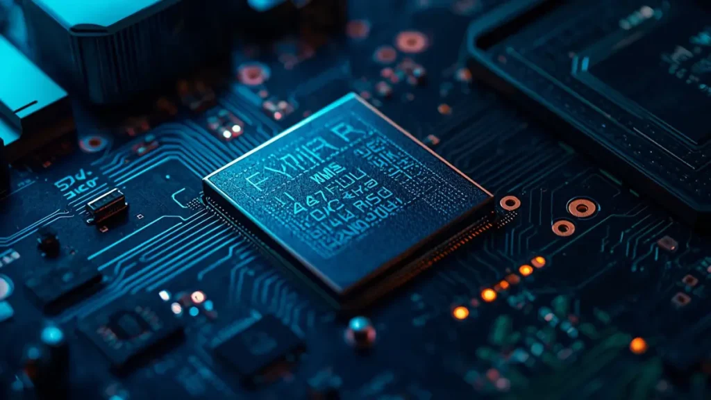
Hongda PCB – High-End AI Motherboard Close-up
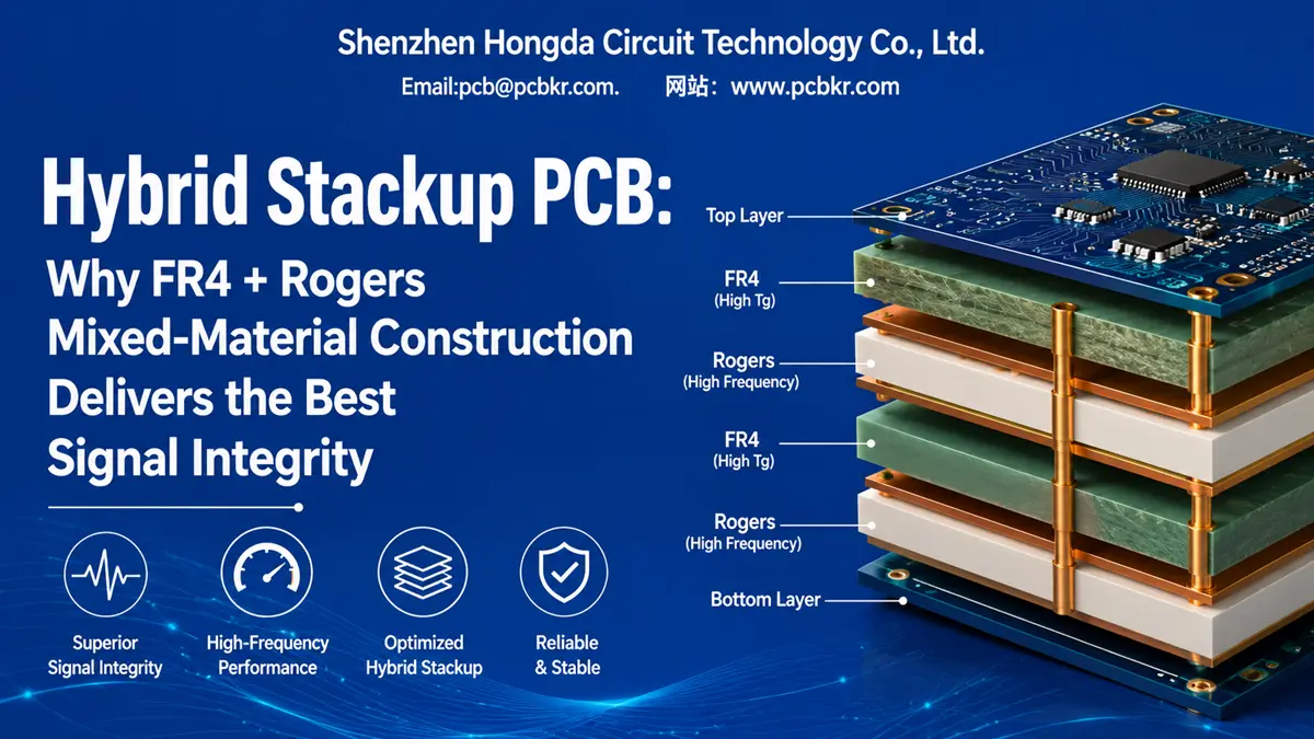
A hybrid stackup PCB, also referred to as a hybrid layer PCB or mixed-dielectric PCB, is a multilayer printed circuit board constructed using two or more distinct laminate materials within a single press cycle. The canonical implementation pairs Rogers or similar low-loss high-frequency laminates on the layers carrying critical high-speed differential pairs, while using standard FR4 on the remaining signal, power, and ground layers.
Anatomy of a Typical FR4 + Rogers Hybrid Stackup
A representative 16-layer hybrid stackup for 112G SerDes design at Shenzhen Hongda Circuit Technology Co., Ltd. might be structured as follows:
- Layers 1 & 2 (Top and Adjacent Signal): Rogers RO4350B, 4 mil core, Dk 3.48, Df 0.0037 — primary high-speed routing layer
- Layers 3–6 (Inner Signal and Plane): FR4 Tg170 — secondary signals, power distribution, and GND reference
- Layers 7 & 8 (Mid-Stack High-Speed): Rogers RO4350B — SerDes lanes requiring low-loss mid-board routing
- Layers 9–14 (Inner Signal and Plane): FR4 Tg170 — power planes, low-speed control signals
- Layers 15 & 16 (Bottom and Adjacent Signal): Rogers RO4350B — bottom-side high-speed interfaces
In this configuration, high-frequency laminate accounts for only 6 of 16 layers, dramatically reducing laminate cost while preserving the signal integrity characteristics required by the high-speed lanes.
Typical hybrid stackup structure: Rogers low-loss layers flanking FR4 core layers in a 16-layer PCB construction
Hybrid Stackup vs. Full Rogers vs. All-FR4: A Direct Comparison
Procurement engineers evaluating PCB sources for high-speed applications need a clear reference for how these three construction approaches compare across the metrics that matter most at production scale.
Full FR4: Lowest material cost, appropriate for signals below 10 Gbps. Insertion loss and fiber-weave effects make it unsuitable for 112G or 224G channels without significant equalization overhead.
Full Rogers/High-Frequency: Maximum signal integrity performance, but 6–9x material cost premium. Justified for mmWave RF, aerospace radar, or test equipment where performance non-negotiable and volume is low.
Hybrid Stackup FR4 + Rogers: Optimal balance for high-speed digital applications. Targets 40–60% material cost reduction versus full-Rogers with signal integrity performance meeting OIF-CEI-112G-VSR and similar specifications.
3. Core Advantages of Hybrid Stackup PCB Technology for 112G and 224G Design
3.1 Insertion Loss and Return Loss Performance Parity with Full-Rogers
The signal integrity case for hybrid stackup construction rests on a straightforward principle: channel loss is dominated by the dielectric through which the signal travels, not by the surrounding layers. A differential pair routed on Rogers RO4350B (Df 0.0037) with proper FR4 ground plane placement beneath it will exhibit insertion loss characteristics functionally equivalent to the same trace in an all-Rogers board — because the field distribution is concentrated in the low-loss Rogers substrate around the trace, not in the FR4 layers above or below it.
- Measured insertion loss on Rogers hybrid signal layers: typically 18–22 dB at 28 GHz for 300 mm trace, within OIF-CEI-112G-VSR compliance window
- Return loss above 15 dB maintained across 0.1–40 GHz frequency range with proper via stub treatment and back-drilling
- Differential skew below 5 ps/inch achievable with low-Df Rogers routing layers, versus 15–20 ps/inch on equivalent FR4 layers
3.2 Material Cost Optimization Without Performance Compromise
Hybrid stackup PCB construction delivers the most significant cost advantage in high-layer-count boards typical of AI server and data center switch designs. Because high-speed laminates are only used on the layers that carry the critical signals, the laminate cost savings scale with the ratio of FR4 to Rogers layers in the stack.
- 6-layer Rogers in a 16-layer hybrid stackup: approximately 38% laminate cost reduction versus all-Rogers
- 4-layer Rogers in a 20-layer hybrid stackup: approximately 56% laminate cost reduction versus all-Rogers
- Production runs of 1,000 to 5,000 units for hyperscale AI hardware: hybrid construction can represent $80,000 to $500,000 in annual BOM savings at board level alone
For engineering teams managing NRE budgets on prototype runs, hybrid stackup designs also reduce prototype cost per panel, enabling more design iterations within a fixed validation budget.
3.3 Design Flexibility for Complex AI and Data Center Architectures
Modern AI server motherboards, GPU interconnect substrates, and high-speed switching ASICs present mixed signal environments where some channels operate at 224G while adjacent interfaces run at PCIe Gen 5 speeds or lower. Hybrid stackup construction allows the PCB designer to allocate dielectric performance precisely to the channel that requires it, rather than over-engineering the entire board.
- GPU-to-GPU NVLink traces can be routed on Rogers layers while PCIe and DDR5 signals share optimized FR4 layers
- Optical module interface PCBs benefit from hybrid construction where the QSFP-DD pad arrays use Rogers layers and the digital control logic uses FR4
- High-speed backplane PCBs for 800G and 1.6T switch chassis combine hybrid stackup with controlled-impedance FR4 for power distribution networks
4. Hybrid Layer PCB Tooling: Manufacturing Process Requirements and Process Control
The engineering advantages of hybrid stackup construction can only be realized through disciplined manufacturing process control. Combining dissimilar laminate materials in a single lamination cycle introduces several process variables that require specific tooling expertise and quality management discipline. This is where supplier selection becomes a critical engineering decision, not just a procurement one.
4.1 CTE Mismatch and Thermal Stress Management in Press Cycle
Rogers RO4350B has a Z-axis coefficient of thermal expansion (CTE) of approximately 46 ppm/°C, while standard FR4 Tg170 laminate runs at 50–70 ppm/°C in the Z-axis. The in-plane (X/Y) CTE of Rogers materials is significantly lower than FR4, typically 14–17 ppm/°C versus 14–18 ppm/°C for FR4, which is close enough to manage. However, the combination of these two materials in a single lamination cycle requires precise control of press temperature profiles to avoid delamination at material interfaces and pad cratering under BGA arrays.
- Press temperature profiles must account for the lower Tg of some Rogers materials (>280°C for RO4350B) versus high-Tg FR4 (170°C Tg, usable to 220°C in reflow)
- Prepreg selection for hybrid bonding layers requires materials with controlled resin flow to avoid Rogers layer distortion during pressing
- Post-lamination dimensional verification using coordinate measurement is mandatory to detect X/Y expansion differential before drilling
4.2 Impedance Control Across Mixed-Dielectric Layer Interfaces
Controlling trace impedance in a hybrid stackup is more complex than in a homogeneous FR4 or Rogers board because the reference plane dielectric changes as signals cross between material zones. Shenzhen Hongda Circuit Technology Co., Ltd. uses field-solver simulation for every hybrid stackup customer design to model the actual Dk profile at each critical layer interface.
- Microstrip impedance on Rogers layers requires recalculation when FR4 prepreg is used as the bonding medium between Rogers and FR4 planes
- Effective Dk at mixed-dielectric interfaces must be modeled as a weighted composite of the two materials present in the field region
- Impedance test coupons must be present on every production panel with layer-specific coupons for both Rogers and FR4 signal layers
4.3 Drilling, Via Formation, and PTH Reliability at Material Interfaces
Drilling through a hybrid stackup presents tool wear and smear removal challenges that differ from single-material boards. Rogers PTFE-based laminates are softer than FR4 and can deform around drill entry points if feed and speed parameters are not optimized for the specific material combination. Electroless copper deposition and plated through-hole reliability must be verified across the Rogers-FR4 interface, where differential resin chemistry can affect adhesion.
- Drill parameters must be validated for each Rogers/FR4 combination using cross-section analysis at first-article stage
- Desmear processes must be qualified for Rogers laminate surfaces, which respond differently to permanganate desmear versus plasma desmear
- Interconnect stress test (IST) or thermal shock testing to IPC-TM-650 2.6.26 should be performed on hybrid stackup designs as part of design qualification
5. How to Design an Effective FR4 + Rogers Hybrid PCB Stackup for 112G/224G Applications
Effective hybrid stackup design requires close collaboration between the PCB designer and the fabrication engineer from the earliest stage of stackup definition. The following engineering guidelines reflect the best-practice methodology used by Shenzhen Hongda Circuit Technology Co., Ltd. in supporting customer designs for 112G and 224G applications.
5.1 Signal Partitioning and Layer Assignment Strategy
The first step in hybrid stackup design is identifying which signals genuinely require low-loss dielectric. Not all high-speed signals need Rogers — the decision should be driven by channel budget analysis, not a blanket material upgrade.
- Run channel simulation (IBIS-AMI or S-parameter based) for each SerDes channel to determine the insertion loss margin available under worst-case process corner
- Assign Rogers layers to channels where insertion loss margin is less than 3 dB above the spec limit — these are the channels where material loss is the binding constraint
- Assign remaining channels to FR4 layers, applying trace width optimization and via stub elimination to minimize dielectric-independent losses
- Allocate power distribution network and ground reference planes to FR4 layers exclusively — there is no signal integrity benefit to Rogers power planes
5.2 Simulation-Driven Stackup Development
Simulation investment at the stackup definition stage pays dividends in reduced prototype iterations. A well-characterized hybrid stackup model allows the design team to predict channel performance before a single panel is fabricated.
- Use 3D EM field solvers (ANSYS HFSS, Cadence EMX, or Keysight ADS) to model via transitions between Rogers and FR4 layers — these transitions are the most common source of unexpected return loss degradation
- Model the actual composite Dk at Rogers-prepreg-FR4 interfaces using material data from the fabricator’s specific laminate stock
- Request S-parameter channel models from the PCB fabricator based on their measured process parameters for hybrid stackup production
5.3 Design for Manufacturability in Hybrid Constructions
Several DFM considerations specific to hybrid stackup construction should be incorporated into the design rules before routing begins.
- Minimum trace width on Rogers layers is typically 2–3 mil wider than FR4 due to the softer material properties affecting etch resolution — confirm with fabricator DFM guidelines
- BGA breakout vias in Rogers areas must account for the different drill-to-copper clearance required for reliable via formation in softer PTFE-based laminates
- Panelization should account for the dimensional stability differences between Rogers and FR4 sections of the hybrid panel during reflow
6. 2026 PCB Manufacturing Technology Advances Enabling Next-Generation Hybrid Stackup
The manufacturing capabilities supporting hybrid stackup PCB production have advanced substantially in the last two years. These developments are relevant to procurement teams evaluating supplier capability for 2026 production programs.
6.1 Any-Layer Via (ALV) and Stacked Micro-Via Integration with Hybrid Materials
The combination of hybrid stackup construction with any-layer interconnect (ALIVH) technology allows high-density via routing in mixed-material boards without the back-drilling requirements that add cost and lead time to traditional through-hole hybrid designs. Several advanced PCB manufacturers, including Shenzhen Hongda Circuit Technology Co., Ltd., qualified ALV processes for hybrid Rogers/FR4 constructions through 2025, enabling denser escape routing from fine-pitch ASICs on hybrid stackup boards.
6.2 Improved Low-Loss Prepreg Materials for Hybrid Bonding Layers
A persistent challenge in hybrid stackup construction has been the use of standard FR4 prepreg as the bonding medium between Rogers signal layers and FR4 core layers. The higher Df of FR4 prepreg created a loss penalty at the bonding interfaces. New low-loss hybrid-compatible prepreg materials introduced in 2024 and 2025 — including modified hydrocarbon-filled systems from Panasonic and Isola — reduce this interface loss contribution by 40–60%, improving channel loss uniformity in hybrid stackup designs.
6.3 Precision Press Temperature Profile Control for Tighter CTE Management
Advanced multi-zone vacuum lamination presses introduced in 2025 allow fabricators to apply different temperature profiles to different zones of a hybrid panel during the press cycle. This capability addresses the fundamental challenge of matching cure requirements for Rogers and FR4 materials in a single press cycle. The result is improved layer-to-layer registration, reduced warpage, and higher first-pass yields on complex hybrid stackup constructions.
6.4 Real-Time Impedance Monitoring and AI-Assisted Process Control
Leading PCB manufacturers now incorporate in-line TDR (Time Domain Reflectometry) measurement at panel level before routing completion, allowing process engineers to identify impedance drift caused by laminate variation within a production lot. When combined with AI-assisted press parameter optimization — trained on historical process data from hybrid stackup production runs — this capability has reduced impedance outliers in hybrid construction panels by approximately 35% compared to conventional SPC-based process control.
7. Primary Applications: Where Hybrid Stackup PCB Construction Delivers Measurable ROI

Hongda PCB – AI Data Center Hardware Infrastructure
7.1 AI Server Motherboards and GPU Interconnect Substrates
The NVIDIA H100 and B200 platforms, AMD MI300X, and competing AI accelerator boards all present hybrid signal environments where NVLink, PCIe Gen 5, and HBM interfaces coexist on the same PCB. Hybrid stackup construction allows GPU server motherboard designers to meet the insertion loss requirements of NVLink 4.0 (operating at 100G per lane) while managing board cost within hyperscaler procurement constraints. Shenzhen Hongda Circuit Technology Co., Ltd. has supported production of AI server motherboards with up to 24-layer hybrid stackup constructions in 2025 and 2026.
7.2 400G and 800G Ethernet Switch ASICs
400G and 800G Ethernet switch line cards present some of the most demanding hybrid stackup design environments, combining 112G PAM4 SerDes channels from switch ASIC to optical cage, PCIe Gen 5 management paths, and DRAM interfaces within a single 24 to 32-layer board. Hybrid construction allows optical cage interfaces to receive Rogers-grade loss performance while internal bus routing remains on cost-optimized FR4 layers.
7.3 High-Speed Backplane and Midplane Assemblies
Backplane PCBs for 800G chassis, where daughter card connectors run at 112G per differential pair, represent the highest-value application for hybrid stackup technology. The combination of large board size (400 mm to 600 mm), high layer count (up to 40 layers), and high-speed connector interfaces creates a channel loss environment where FR4 alone is insufficient but full-Rogers cost is prohibitive. Hybrid backplane constructions using Rogers layers adjacent to connector footprints and FR4 for mid-board power distribution represent the current industry standard for this application.
7.4 Optical Transceiver PCBs and PAM4 DSP Interface Boards
Coherent optical transceivers and PAM4 DSP interface boards operate at signal frequencies extending above 60 GHz at the electrical interface. These applications frequently use hybrid stackup construction with ultra-low-loss Rogers or PTFE-based laminates on RF and microwave signal layers while using FR4 for digital control and power sections. The relatively small board size in these applications means the cost delta between hybrid and full-Rogers is modest, but hybrid construction still provides advantage in standardizing FR4-compatible assembly processes for SMT.
8. When to Choose Hybrid Stackup vs. Full High-Frequency Laminate PCB Construction
The decision framework for choosing between hybrid stackup and full high-frequency laminate construction depends on four primary factors that should be evaluated systematically before releasing a design to fabrication.
8.1 Channel Loss Budget Analysis
If channel simulation shows that insertion loss with FR4 on critical layers exceeds the SerDes receiver equalization range by more than 4–5 dB, and that range cannot be recovered by trace routing optimization, a Rogers layer is warranted. If the insertion loss exceeds the equalization range by less than 2 dB, FR4 optimization (shorter traces, via back-drilling, wider differential pair spacing) may achieve compliance without a hybrid construction penalty.
8.2 Signal Density and Mixed-Speed Interface Ratio
Hybrid stackup delivers the highest ROI when the board contains a significant ratio of lower-speed to high-speed signals. Boards where more than 70% of signals operate above 25 Gbps per lane may find that the complexity and cost premium of hybrid tooling approaches that of a full-Rogers construction. Boards where high-speed channels represent 30–50% of total signal routing are the ideal candidates for hybrid construction.
8.3 Production Volume and Unit Cost Sensitivity
At prototype quantities below 20 units, the tooling cost of hybrid layer PCB manufacturing can reduce the per-unit cost advantage of the hybrid approach. At quantities above 100 units, hybrid construction almost always delivers net cost savings relative to full-Rogers construction. Shenzhen Hongda Circuit Technology Co., Ltd. offers hybrid stackup from prototype through mass production, with engineering support available from stackup definition through production qualification.
8.4 Schedule and Supply Chain Considerations
Hybrid stackup PCBs require longer lead times than single-material boards due to the multi-step lamination cycle and additional process qualification requirements. Typical lead times at Shenzhen Hongda Circuit Technology Co., Ltd. for hybrid stackup prototypes are 10–15 business days, with production lead times of 20–28 days depending on layer count and material availability. Rogers material lead times from distributors should be confirmed before finalizing the design schedule.
9. Selecting a Hybrid Stackup PCB Manufacturer: Key Supplier Qualification Criteria
Choosing the right manufacturing partner for hybrid stackup PCB production is as important as getting the design right. The following qualification criteria help procurement teams and engineering managers evaluate suppliers objectively.
- Documented experience with hybrid Rogers/FR4 constructions at or above the target layer count, supported by customer references or published case studies
- In-house impedance testing capability with TDR and VNA, with hybrid-stackup-specific coupon designs confirmed by the fabricator
- Cross-section analysis capability for first-article qualification, with demonstrated ability to characterize Rogers-FR4 interface quality
- IPC Class 2 or Class 3 certification with evidence of compliance in hybrid stackup production, not just single-material boards
- Field solver simulation support for stackup development — fabricators who cannot model composite Dk at mixed-dielectric interfaces should not be trusted with 112G hybrid designs
- DFM review process that specifically addresses hybrid construction constraints including Rogers trace width adjustment, via formation parameters, and panelization rules
About Shenzhen Hongda Circuit Technology Co., Ltd.: Hongda is a specialist PCB manufacturer based in Shenzhen with production capability for multilayer hybrid stackup constructions from 4 to 40 layers. Our engineering team provides signal integrity simulation support, stackup development, and DFM review for hybrid FR4 + Rogers designs targeting 112G and 224G applications. Contact our engineering team for a hybrid stackup design review and quotation.
10. Conclusion: Hybrid Stackup PCB as the Engineering-Optimal Solution for High-Speed Design in 2026
Hybrid stackup PCB construction, combining FR4 and low-loss high-frequency laminates in a single multilayer board, represents the most practical path to 112G and 224G signal integrity compliance for commercial-scale AI server, networking, and data center hardware. By concentrating material investment at the physical layers where signal loss physics demand it, hybrid stackup construction delivers channel insertion loss and return loss performance functionally equivalent to full-Rogers designs at 40–60% lower material cost.
The manufacturing maturity of hybrid layer PCB tooling has reached the point where qualified fabricators can deliver hybrid stackup boards with impedance control to ±7%, reliable PTH in mixed-material constructions, and layer registration suitable for fine-pitch ASIC BGA interfaces. The 2025–2026 introduction of low-loss hybrid bonding prepregs and AI-assisted press control has further improved process yields and design predictability.
For design teams planning 112G or 224G PCB designs in 2026, the key engineering decisions are clear: identify your channel loss-critical layers through simulation, specify Rogers or equivalent low-loss laminate only on those layers, engage your PCB fabricator during stackup definition rather than after layout completion, and qualify your supplier on demonstrated hybrid construction capability — not just single-material PCB experience.
Shenzhen Hongda Circuit Technology Co., Ltd. is available to support hybrid stackup designs from initial stackup consultation through volume production. Engineers can submit their layer stack requirements and net list for a no-commitment stackup development and DFM review.
FAQs
What is the typical price premium for hybrid stackup PCB versus standard FR4 construction at the same layer count?
The price premium for hybrid stackup construction versus all-FR4 at the same layer count depends primarily on the number of Rogers layers and the Rogers material grade specified. In typical 16–24 layer hybrid stackup designs with 4–8 Rogers layers, procurement teams should budget a 30–55% price increase over equivalent all-FR4 construction. This compares to a 350–550% price increase for equivalent full-Rogers construction. The actual unit price is highly sensitive to Rogers material grade (RO4003C versus RO4350B versus Megtron 7 carry different costs), number of press cycles required, panel utilization, and production volume. Shenzhen Hongda Circuit Technology Co., Ltd. provides fixed-cost quotations for hybrid stackup designs with full BOM transparency for laminate, prepreg, and process costs.
What certifications should a hybrid stackup PCB supplier hold, and how do I verify actual production experience?
Minimum baseline certifications for hybrid stackup PCB suppliers serving commercial data center and AI server applications include IPC-6012 Class 2 or Class 3 (dependent on application), ISO 9001:2015, and UL recognition for the laminate materials used in production. For suppliers targeting aerospace or defense applications, AS9100D or MIL-PRF-31032 certification is required. Verifying actual hybrid production experience beyond certification requires requesting cross-section photographs from completed hybrid stackup panels, insertion loss measurement data from coupon testing on hybrid constructions, and reference contacts from customers with active hybrid stackup production programs. Suppliers who can only provide general PCB certifications without material-specific process qualification data for Rogers-FR4 hybrid construction should be treated with caution.
How long does first-article qualification take for a new hybrid stackup design, and what does the process include?
First-article qualification for a hybrid stackup PCB design at Shenzhen Hongda Circuit Technology Co., Ltd. typically takes 4 to 6 weeks and includes the following process steps: stackup development with field-solver simulation, DFM review and design rule verification, first-article panel fabrication, cross-section analysis at Rogers-FR4 interface layers, impedance measurement on all signal layer coupons using TDR to IPC-2141A methodology, electrical continuity and isolation testing to IPC-TM-650, visual and dimensional inspection to IPC-A-600 Class 2 or 3, and test report package delivery. For designs targeting IPC Class 3 per IPC-6012, interconnect stress testing and thermal shock cycling are added to the qualification flow. Procurement teams should build first-article qualification lead time into program schedules as a separate milestone from prototype board delivery.
What is the minimum order quantity for hybrid stackup PCB production, and how does pricing scale with volume?
Most specialized hybrid stackup manufacturers, including Shenzhen Hongda Circuit Technology Co., Ltd., accept orders from single-unit prototype through full production volume. Prototype pricing for hybrid stackup designs typically applies to orders of 1–10 panels, with price breaks at 10–50 panels (low-volume production pricing), 50–500 panels (mid-volume), and 500+ panels (production volume). The per-unit cost reduction from prototype to production volume in hybrid stackup designs is typically 45–65%, reflecting the amortization of tooling setup, lamination fixtures, and process qualification costs across a larger production run. For annual production programs, blanket purchase orders with monthly call-off schedules can reduce unit pricing by an additional 8–15% relative to individual purchase order pricing at the same monthly quantity.
Can a hybrid stackup PCB manufacturer support both NPI prototype and mass production from the same facility, and why does that matter?
Sourcing both NPI and production from the same hybrid stackup fabricator is strongly advisable for high-speed PCB designs. The process parameters developed during first-article qualification — press temperature profiles, drill parameters, prepreg selection, impedance control settings — are facility-specific and line-specific. When a design transfers from an NPI specialist to a different production fabricator, these parameters must be re-qualified from scratch, typically adding 4–6 weeks to production ramp and introducing a new source of process variation at exactly the point in the program where schedule pressure is highest. Shenzhen Hongda Circuit Technology Co., Ltd. operates prototype and production capability within the same facility, using the same qualified process parameters from first prototype through volume production. This continuity eliminates the most common cause of yield surprises in hybrid stackup production ramp.
About Author
David Chen https://www.linkedin.com/in/pcbcoming
David Chen boasts an extensive professional background in PCBA manufacturing, PCBA testing, and PCBA optimization, with specialized expertise in high-precision PCBA fault analysis and rigorous PCBA reliability testing. The author has worked with high-layer-count server PCB fabrication, ultra-low-loss backplane stackups, and thermo-mechanical reliability optimization for AI infrastructure projects involving 112G and 224G PAM4 architectures. Skilled in complex circuit design and cutting-edge advanced PCB manufacturing processes, he delivers solutions that elevate product durability and performance across industrial applications. His technical articles focusing on PCBA manufacturing workflows and testing methodologies are widely cited by industry peers, research institutions, and technical platforms, solidifying his reputation as a recognized technical authority in the global circuit board manufacturing sector.
Recommended: Explore the full High Speed PCB Manufacturing guide for detailed insights.