Copper Base PCB vs Aluminum Base PCB in 2026: The MetalClad PCB Manufacturing Guide for High-Power Design
Copper Base PCB vs Aluminum Base PCB are the two core categories of metal-clad PCB technology that address the critical thermal bottlenecks of modern electronics. In 2026, power density has become the definitive constraint dominating electronics design across all high-performance application scenarios. AI server racks, SiC/IGBT inverters, automotive LED headlamp modules, as well as 5G and emerging 6G RF power amplifiers, are all evolving toward a core design trend: delivering higher power output within a shrinking printed circuit board area.
This extreme upgrade in power density poses an unprecedented heat dissipation challenge for traditional circuit board materials. Standard FR4 PCB substrates can no longer conduct and dissipate high-intensity heat at a sufficient speed, easily leading to overheating, performance degradation and reduced service life of high-power electronic devices.
Against this industry backdrop, metal-clad PCBs, mainly divided into copper base PCB and aluminum base PCB variants, have successfully transitioned from a niche thermal management alternative to a mainstream and indispensable manufacturing solution. For current electronics design and procurement teams, selecting and applying the right copper base PCB and aluminum base PCB solutions accurately on the first try has become a core requirement to ensure the stability, reliability and performance of 2026 high-power electronic products.
At Shenzhen Hongda Circuit Technology Co., Ltd., we build both aluminum base PCB and
copper base PCB (including direct-thermal-path copper base PCB) for customers who
cannot afford a thermal failure in the field. This guide breaks down what actually separates
a copper based PCB from an aluminum base PCB, how the numbers should be measured
and compared in the first place, when copper is genuinely worth its premium, and how to
choose the correct metal substrate for your 2026 production program.
Why Metal-Clad PCB Technology Is Central to 2026 PCB Manufacturing
Three forces are reshaping metal base PCB demand this year. AI data-center power
supplies and busbars are driving unprecedented current density per board. Electric vehicle
DC-DC converters and onboard chargers are moving to SiC and IGBT power modules that
dump heat in tiny, concentrated hotspots. And 5G/6G base-station power amplifiers keep
shrinking the footprint while raising output power. Each of these applications turns a
standard FR4 layout into a thermal bottleneck long before it becomes an electrical one.
The result is that “PCB manufacturing technology” conversations in 2026 increasingly start
with the substrate, not the copper trace. Insulated metal substrate (IMS) boards — the
umbrella term covering both aluminum base PCB and copper base PCB — are no longer a
specialty add-on; they are the default starting point for any design exceeding roughly 10
W/cm² of local power density.
Clearing Up the Biggest Myth in Metal Substrate PCB Design
Most sourcing conversations assume that swapping an aluminum base for a copper base
automatically delivers a dramatic thermal upgrade, because pure copper conducts heat
roughly seven times better than aluminum. In practice, the metal base is rarely the
bottleneck. The component that actually decides whether your board can dissipate heat is
the dielectric layer sandwiched between the copper circuit foil and the metal base.
Whatever thermal advantage the base metal has on paper gets throttled the moment heat
has to cross that insulating layer.
Copper Base PCB vs Aluminum Base PCB: Where the Real Thermal Path Bottleneck Sits
Strip away the marketing and the two board families share an identical stack-up: copper foil
circuit layer, dielectric (insulating) layer, then the metal base — either aluminum or copper.
Standard Aluminum Base PCB and Copper Based PCB Thermal Conductivity Compared
With a conventional dielectric layer in place, a standard aluminum base PCB typically
delivers an overall thermal conductivity of only 1.0–4.0 W/m·K. A standard copper based
PCB, built with the same style of dielectric, reaches roughly 4.0–12.0 W/m·K. That is a real,
meaningful improvement — but it is nowhere near the 398 W/m·K that pure copper
achieves in isolation. The dielectric layer effectively caps copper’s native performance,
which is the detail most datasheets gloss over.
Direct Thermal Path (DTP) Copper Base PCB: The Technology That Actually Unlocks Copper’s Advantage
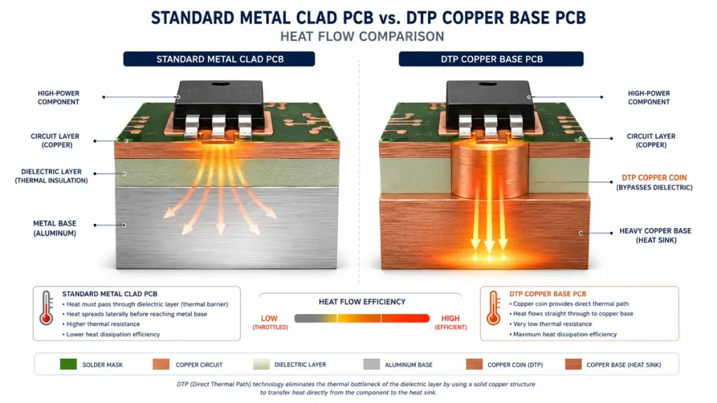
Cross-section comparison showing how a true DTP copper base PCB bypasses the dielectric layer with an embedded copper coin to achieve 380+ W/m·K, whereas a standard substrate remains bottlenecked by the insulating layer.
Copper base PCB earns its reputation only when paired with direct thermal path (DTP)
construction — sometimes called embedded copper coin or copper bump technology. Here,
a solid copper insert is machined and bonded directly beneath the high-power component
pad (an automotive LED die, a power MOSFET, an IGBT), physically bypassing the
dielectric layer altogether. Under a true DTP copper base PCB structure, the local thermal
path can approach the 380+ W/m·K performance of solid copper — a jump that a standard
aluminum base PCB has no process route to match, because aluminum cannot be
machined and bonded with the same precision for embedded thermal coins.
This is the one capability gap that should decide the metal choice on its own: if your design
needs a local heat spreader machined straight into the base, you need copper base PCB
manufacturing, not aluminum.
Testing and Comparison Methodology: How These Numbers Are Actually Measured
Thermal and mechanical specifications for metal base PCB are only meaningful if the test
conditions behind them are known. Before comparing any two vendor datasheets — or the
figures in this guide — against each other, confirm the following variables are aligned:
1.Thermal conductivity test method. Dielectric-layer thermal conductivity is normally
reported per ASTM D5470 (steady-state, guarded hot-plate method) on the isolation
material alone, not on the finished board. A “board-level” thermal resistance figure
(°C/W or °C·in²/W) is a different, and usually more useful, number — it must state the
copper foil weight, dielectric thickness, and base metal thickness used in the test
coupon, because changing any one of those shifts the result.
2. Base metal and dielectric thickness. Reported conductivity ranges (e.g. 1.0–4.0
W/m·K for aluminum base PCB) assume a specific dielectric thickness, commonly in
the 75–150µm range. Thinner dielectric improves thermal performance but reduces
dielectric breakdown voltage and increases capacitive coupling — always request the
dielectric thickness alongside any conductivity claim.
3. Board thickness and copper weight. A 1.0mm vs 1.6mm vs 2.0mm aluminum or
copper base changes the total thermal spreading resistance, not just the weight.
Copper foil weight (1oz / 2oz / 3oz+) affects in-plane heat spreading before heat ever
reaches the dielectric layer, so two boards with identical base metal can behave
differently at the same power level.
4. Test environment. Reported CTE (coefficient of thermal expansion) values are
typically measured across a specific temperature range (commonly -40°C to +125°C
for automotive-grade material) — a CTE figure quoted without a stated range is not
directly comparable across suppliers.
5. Sample condition and DTP geometry. For DTP copper base PCB, the 380+ W/m·K
local figure applies specifically at the embedded copper coin location, under a defined
coin diameter and depth. It is not the thermal conductivity of the board as a whole,
and quoting it as a blanket board-level number is a common (and misleading)
shortcut in supplier marketing.
When requesting quotes or datasheets, ask suppliers to specify dielectric thickness, base
thickness, copper weight, and test standard alongside any thermal number — an isolated
W/m·K figure without those four data points cannot be used for an apples-to-apples
comparison.
Full Technical Comparison: Copper Base PCB vs Aluminum Base PCB
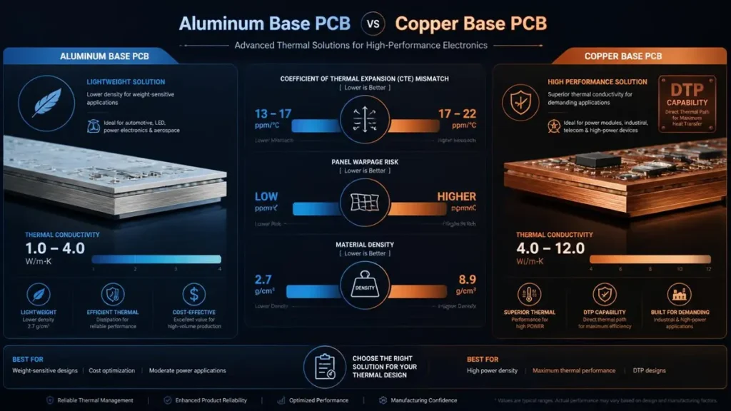
Key engineering trade-offs between aluminum and copper substrates, highlighting differences in thermal conductivity, CTE matching, weight, and warpage risks during production.
| Comparison Factor | Aluminum Base PCB | Copper Base PCB | Engineering / Procurement Takeaway |
|---|---|---|---|
| Dielectric-layer thermal conductivity | 1.0–4.0 W/m·K | 4.0–12.0 W/m·K (standard) | With a dielectric layer in the path, copper’s advantage is a multiple, not an order of magnitude |
| DTP / embedded copper coin capability | Not achievable at production precision | Fully supported (DTP bump, embedded copper block) | Local power density above roughly 30 W/cm² effectively mandates copper base PCB |
| Coefficient of thermal expansion (CTE) | ~22 ppm/°C — larger mismatch with copper foil and die | ~17 ppm/°C — closely matched to copper circuitry | Copper base PCB solder joints resist fatigue better under repeated thermal cycling |
| Machining and warpage behavior | Easy to route, V-cut, and de-panel; low warpage risk | Dense material, heavy tool wear, prone to warping in large panels | Copper base PCB manufacturing needs tighter router and V-score process control |
| Density / weight | Lightweight — 2.7 g/cm³ | Heavy — 8.9 g/cm³, roughly 3.3× aluminum | Weight-critical designs (aerospace, drones, handhelds) should default to aluminum base PCB |
When Copper Base PCB Is Genuinely Worth It — and When It Is Just a More Expensive Aluminum Board
Copper’s raw thermal conductivity advantage over aluminum is real, but it only translates
into a meaningful system-level benefit under specific conditions. Outside of those
conditions, a copper base PCB is simply a heavier, slower-to-source, more expensive
version of an aluminum board delivering the same practical result.
Copper base PCB is genuinely superior when:
1. The design requires a DTP embedded copper coin or bump, because aluminum has no
equivalent process — this is the one case where the gap is categorical, not incremental.
2. Local power density at the hotspot exceeds roughly 30 W/cm², where a dielectric-only
thermal path (whether aluminum or copper base) starts to push junction
temperatures past safe margins.
3. The product will see frequent, wide thermal cycling (automotive underhood, outdoor
base stations, cold-chain equipment), where copper’s closer CTE match to copper
circuitry measurably reduces solder-joint fatigue over the product’s service life.
Copper base PCB delivers limited real-world benefit when:
1. The board uses a standard dielectric layer (no DTP) and total power dissipation is moderate — the 4.0–12.0 W/m·K standard copper figure is better than aluminum’s 1.0
4.0 W/m·K, but rarely enough to change a thermal design that was already marginal on aluminum. In these cases, adding an external heatsink or improving airflow to an
aluminum base PCB is usually more cost-effective than switching substrates.
2. Weight, panel size, or warpage tolerance is a hard constraint — copper’s density and
machining behavior work directly against those requirements regardless of thermal upside.
3. Budget and lead time are the binding constraints and the thermal margin on aluminum, even if tight, still meets the design’s junction-temperature spec with a reasonable derating.
The practical rule: copper base PCB is a targeted solution for a specific thermal bottleneck
(usually solved through DTP), not a general-purpose upgrade over aluminum base PCB.
Engineering Case Studies
The following cases illustrate typical outcomes seen in DTP copper base PCB and standard
aluminum base PCB programs. Figures are representative of common results in these
application classes and should be validated against your own design’s power profile and
test conditions using the methodology above.
Case Study 1: Automotive High-Beam LED Headlamp Module (DTP Copper Base PCB)
A high-brightness automotive LED headlamp module concentrates several watts of
dissipation into an LED footprint smaller than 3mm × 3mm — well above the 30 W/cm²
threshold where a dielectric-only thermal path becomes the limiting factor.
1.Baseline (standard aluminum base PCB, dielectric-only path): junction-to-base
thermal resistance in the range of 3.5–5.0 °C/W is typical, which pushes LED junction
temperature close to its rated maximum under sustained high-beam operation,
shortening lumen-maintenance life.
2. DTP copper base PCB (embedded copper coin directly beneath the LED pad):
junction-to-base thermal resistance typically drops to 0.8–1.5 °C/W, because the
dielectric layer is bypassed at the hotspot entirely.
3. Practical effect: a lower and more stable junction temperature under continuous
high-beam operation, which is why DTP copper base PCB has become close to a
default requirement for automotive high-power LED modules rather than an optional
upgrade.
Case Study 2: EV DC-DC Converter Power Module (Copper Base PCB vs Aluminum Base PCB)
An onboard EV DC-DC converter using an IGBT/SiC power stage was evaluated on both a
standard aluminum base PCB and a copper base PCB, both without DTP, to isolate the
effect of the base metal alone.
1. Standard aluminum base PCB: board-level thermal resistance measured in the 1.2
1.8 °C·in²/W range at the power-device mounting area under continuous rated load.
2. Standard copper base PCB (no DTP): board-level thermal resistance improved to
roughly 0.6–1.0 °C·in²/W under the same test conditions — a meaningful but incremental improvement, consistent with the standard 4.0–12.0 W/m·K dielectric layer figure rather than copper’s bulk conductivity.
3. Practical effect: this level of improvement was enough to bring the design within its
thermal derating margin without adding DTP, illustrating the “moderate benefit, moderate cost” case described above — copper base PCB was justified here by thermal-cycling reliability requirements (frequent power cycling in EV duty cycles) as much as by raw thermal performance.
Selecting the right substrate is only half the sourcing decision. The supply chain behavior of aluminum base PCB and copper base PCB is genuinely different, and it changes program timing.
Heavy Copper PCB Base Material Availability and Lead Time
Aluminum base copper-clad laminate (CCL) is a commodity material stocked broadly
across the supply chain. Heavy copper PCB base material and DTP-grade copper laminates,
by contrast, are typically sourced from a narrower set of major laminate suppliers in specific
constructions, and lead times commonly run two to three weeks longer than an equivalent
aluminum program.
MOQ and Prototyping Cost Differences
Aluminum base PCB prototyping generally carries little to no minimum order quantity.
Copper base PCB, because the raw laminate is expensive and panel utilization is less
forgiving, more often comes with a minimum order requirement and a higher NRE cost at
the prototype stage.
Surface Finish for Copper Base PCB and Aluminum Base PCB Backside Protection
A common oversight: the top-side circuit finish (ENIG, OSP, immersion silver) is not the
same process as the metal base backside treatment. A copper base PCB backside typically
needs a dedicated nickel plating, bead-blast, or chemical passivation step to prevent
oxidation in storage, while an aluminum base PCB backside is more commonly passivated
or simply brushed.
Application Fit: Where Aluminum Base PCB and Copper Base PCB Actually Belong
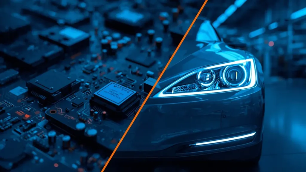
Industrial application split—cost-effective aluminum substrates excel in high-volume general LED lighting, while high-reliability DTP copper substrates are mandatory for 2026 EV power modules and automotive matrix headlamps.
Aluminum Base PCB for High-Volume, Cost-Sensitive Thermal Management
Aluminum base PCB remains the correct default for general LED lighting (street lighting,
industrial high-bay fixtures, backlighting strips), consumer-grade switching power
supplies, and industrial VFD driver boards — anywhere a moderate thermal budget meets a
volume-driven cost target.
Copper Base PCB (DTP) for Extreme Power Density and Reliability
Copper base PCB, and specifically DTP copper base PCB, is the correct choice for
automotive high-brightness LED headlamp modules, EV high-voltage DC-DC converters
and inverters built around IGBT/SiC power modules, and 5G/6G base-station RF power
amplifiers — applications where the cost of a thermal failure vastly outweighs the material
premium of copper.
4-Step Decision Framework for Selecting Metal Base PCB Manufacturing Technology
y
- Measure local power density. Does the hotspot under your component exceed what a
dielectric-layer-only thermal path can absorb? If a DTP structure is required, copper
base PCB is mandatory, not optional. - Assess the thermal-cycling environment. Will the board see repeated, severe
temperature swings — automotive underhood, military, or outdoor arctic exposure? If
solder-joint reliability under thermal cycling is critical, copper base PCB’s closer CTE
match is the safer choice. - Check your supply-chain timeline. Is this an expedited prototype run or an
extremely cost-constrained production build? If schedule or budget dominates,
aluminum base PCB paired with external active cooling is usually the pragmatic
answer. - Confirm mechanical constraints. Does the end product have strict weight or board
warpage tolerances? Copper’s density and warpage behavior can rule it out even
when the thermal case favors it.
Design Parameters: 2oz Copper Base Metal PCB, 3oz Copper Aluminum Base PCB, and Multilayer Builds
Metal base PCB specifications are frequently defined by copper weight and base thickness
rather than by substrate type alone. A 2oz copper base metal PCB adds current-carrying
capacity on top of the thermal path, which is common in power-conversion layouts. An
aluminum base PCB 3oz copper build is a frequent middle-ground spec for driver boards
that need both moderate heat spreading and heavier trace current handling. Multilayer
metal base PCB (double-sided or true multilayer aluminum/copper base construction) is
achievable but comes with blind/buried via constraints and a real cost premium.
Frequently Asked Questions About Copper Base PCB and Aluminum Base PCB Manufacturing
What is the typical MOQ for copper base PCB versus aluminum base PCB?
Aluminum base PCB generally has little or no minimum order quantity, even at the prototype stage. Copper base PCB, due to laminate cost and lower panel utilization, more commonly carries a minimum order requirement and higher first-article cost — confirm this at quoting stage
if you are ordering small pilot batches.
How much longer is the lead time for copper base PCB?
Copper base PCB, especially DTP-grade or heavy copper builds, typically adds two to three weeks to lead time compared with an equivalent aluminum base PCB program, mainly due to a narrower base of qualified
laminate suppliers for these constructions.
Do copper base PCB and aluminum base PCB use the same surface finish process?
Only on the top-side circuit layer (ENIG, OSP, immersion silver, etc.). The metal base backside is a separate process: copper base PCB backsides commonly need nickel plating, bead blasting, or chemical passivation to prevent storage oxidation, while aluminum base PCB backsides are more often simply passivated or brushed.
Can metal base PCB be built as double-sided or multilayer boards?
Yes, though multilayer aluminum or copper base PCB is constrained by blind- and buried-via processing limits and carries a meaningful cost premium over single-layer builds — this should be confirmed with your manufacturer during the design stage, not after tooling is committed.
What routing restrictions apply to a DTP copper base PCB?
The embedded copper coin or bump location dictates a minimum insulation clearance from surrounding circuit traces, so DTP placement needs to be locked in before final routing rather than treated as a late stage layout change. The coin diameter and depth also constrain how close adjacent vias and traces can sit to the hotspot.
How do I decide on base metal thickness — 1.0mm, 1.6mm, or 2.0mm?
Base thickness is chosen against the required thermal spreading area, mechanical rigidity for the panel size, and connector or mounting-hardware clearance — thicker bases spread heat over a wider area but add weight and reduce routing flexibility at the panel edge.
Manufacturing Partner: Shenzhen Hongda Circuit Technology Co., Ltd.
Shenzhen Hongda Circuit Technology Co., Ltd. manufactures both aluminum base PCB
and copper base PCB, including DTP embedded-copper-coin construction, heavy copper
base builds up to 3oz+, and multilayer metal substrate PCB, with process control tuned
specifically for the machining, warpage, and backside-finish challenges outlined above. For
engineering teams evaluating 2026 PCB manufacturing technology for high-power, high
reliability programs, our team can review your thermal budget, application environment,
and volume plan against the decision framework above and recommend the correct
substrate before you commit to tooling.
About Author
David Chen https://www.linkedin.com/in/pcbcoming
David Chen boasts an extensive professional background in PCBA manufacturing, PCBA testing, and PCBA optimization, with specialized expertise in high-precision PCBA fault analysis and rigorous PCBA reliability testing. The author has worked with high-layer-count server PCB fabrication, ultra-low-loss backplane stackups, and thermo-mechanical reliability optimization for AI infrastructure projects involving 112G and 224G PAM4 architectures. Skilled in complex circuit design and cutting-edge advanced PCB manufacturing processes, he delivers solutions that elevate product durability and performance across industrial applications. His technical articles focusing on PCBA manufacturing workflows and testing methodologies are widely cited by industry peers, research institutions, and technical platforms, solidifying his reputation as a recognized technical authority in the global circuit board manufacturing sector.