Aerospace PCB Solutions: Materials,Testing, Design Standards, and Manufacturing Excellence for Mission-Critical Electronics
Avionics PCB and other printed circuit boards for the aerospace and defense electronics industry must withstand extreme conditions unmatched by commercial products—temperature swings from cryogenic cold to re-entry heat, vacuum environments where standard materials release volatile contaminants that ruin missions, and intense vibration spectra capable of cracking solder joints within seconds. At Shenzhen Hongda Circuit Technology Co., Ltd., we tailor our manufacturing and engineering expertise to solve these harsh operating challenges. Our Shenzhen factory holds AS9100D certification, ISO9001 quality management systems and IATF16949 automotive-standard process control, manufacturing 4-layer prototype boards up to 28-layer high-density interconnect (HDI) circuits for satellites, aircraft avionics and defense equipment.
This guide consolidates the technical knowledge, standards, and procurement intelligence that design engineers and supply chain professionals need when sourcing aerospace PCBs. It covers material selection, reliability testing, design compliance, space-grade requirements, avionics applications, and the practical questions buyers ask when qualifying a supplier.
Aerospace PCB Materials: Selecting High-Reliability Materials for Extreme Environments
High-Reliability Avionics Rigid-Flex PCB for Aerospace Applications
When engineers design electronics for aircraft, satellites, and defense systems, the choice of aerospace PCB materials directly determines whether a mission succeeds or fails. Unlike consumer-grade boards, aerospace printed circuit boards must survive temperature swings from -55°C to +125°C, intense vibration during launch, and vacuum conditions that accelerate material degradation. At Shenzhen Hongda Circuit Technology, we have spent years refining material selection protocols that align with NASA, ESA, and MIL-PRF-31032 requirements, ensuring every laminate, resin, and copper foil performs under stress.
What Materials Are Used in Aerospace PCBs?
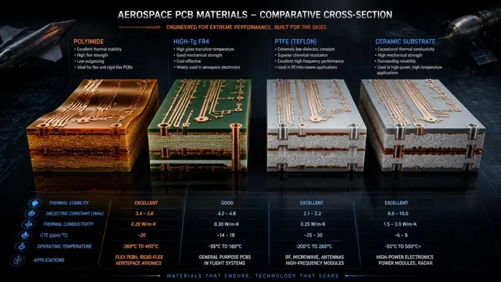
The aerospace PCB material landscape has evolved far beyond standard FR-4. Modern mission-critical electronics demand substrates that balance thermal stability, outgassing control, and signal integrity across multiple frequency bands.
Polyimide PCB Materials for Aerospace Applications
Polyimide aerospace PCB substrates remain the gold standard for flexible and rigid-flex circuits in aviation and space. With glass transition temperatures (Tg) exceeding 200°C and decomposition temperatures above 500°C, polyimide films such as DuPont Pyralux and Rogers RO3003 (PTFE-based high frequency laminate) withstand repeated thermal cycling without delamination. In our Shenzhen facility, we process adhesiveless polyimide constructions that achieve Total Mass Loss (TML) below 0.5% and Collected Volatile Condensable Material (TML ≤1.0 %) (CVCM ≤0.1 %). This makes polyimide ideal for satellite payload boards where outgassing contamination could blind optical sensors or degrade RF performance.
High Tg FR4 Materials for Cost-Sensitive Avionics
Not every aerospace application requires polyimide. For commercial avionics and UAV control systems, high Tg FR4 materials offer a pragmatic middle ground. We specify Isola 370HR and Nelco N4000-13 epoxy-glass laminates with Tg values above 170°C and low Z-axis expansion coefficients. These materials pass IPC-6012 Class 3 qualification while remaining cost-competitive for medium-reliability programs. Our process upgrades include high-performance ultra-low-loss copper-clad laminates (CCL) with low dielectric constant (Dk) and dissipation factor (Df) at 10 GHz, reducing signal attenuation compared to legacy systems. This capability is enabled by our Lauffer lamination system, which maintains precise temperature and pressure profiles across large-format panels.
PTFE and Ceramic-Filled Substrates for RF Aerospace PCBs
Radar, communication arrays, and electronic warfare systems push frequencies into millimeter-wave territory. PTFE aerospace PCB materials—including Rogers RO3003, RT/duroid 6002, and Arlon CLTE-XT—deliver stable dielectric properties across temperature and humidity extremes. Ceramic-filled PTFE variants further improve thermal conductivity, enabling heat dissipation in vacuum environments where convection cooling does not exist. Our engineering team routinely stacks PTFE RF layers with high-Tg FR4 digital layers in hybrid constructions, optimizing both signal integrity and mechanical rigidity.
Ceramic-Based Materials for High-Power Aerospace Electronics
Power distribution modules and motor controllers in electric aircraft generate substantial heat. Ceramic PCB materials such as aluminum oxide (Al₂O₃) and aluminum nitride (AlN) offer thermal conductivities exceeding 170 W/m·K—orders of magnitude higher than FR-4. While ceramic boards require specialized laser machining and metallization, their ability to operate at high temperatures makes them irreplaceable for high-power aerospace applications.
Why Is Polyimide Widely Used in Aerospace PCB Manufacturing?
Procurement teams and design engineers consistently specify polyimide for four fundamental reasons that no other material class fully satisfies simultaneously.
High Temperature Resistance in Aerospace Environments
Polyimide maintains mechanical integrity across the full military temperature range (-55°C to +125°C) and extends operational capability under continuous exposure. This matters when PCBs mount near jet engines, power amplifiers, or re-entry vehicle heat shields. Our lamination presses apply precise temperature and pressure profiles—180–200°C at 200–300 psi—to ensure polyimide layers bond without resin starvation or void formation.
Low Outgassing Performance for Space-Grade PCBs
In orbital vacuum, every organic material releases volatile compounds. Standard FR-4 can exhibit TML of 1.2% and CVCM of 0.15%—levels that condense onto optical lenses, solar panels, and RF antennas. We pre-bake all polyimide raw materials per IPC-1601 protocols and validate every lot through ASTM E595 testing. This disciplined approach has supported multiple LEO satellite programs where optical contamination would terminate the mission.
Mechanical Stability Under Vibration and Shock
Aerospace launch profiles impose random vibration spectra from 20 Hz to 2000 Hz with power spectral densities exceeding 0.04 g²/Hz. Polyimide’s tensile strength—typically 200–300 MPa—prevents trace cracking and pad lifting under these loads. Our rigid-flex designs further distribute mechanical stress by replacing connector assemblies with continuous copper interconnects, eliminating failure-prone solder joints and crimp contacts.
Long Service Life for Extended Missions
Deep-space probes and geostationary satellites must operate for 15–20 years without maintenance. Polyimide’s resistance to radiation-induced chain scission and oxidative degradation supports these timelines. We complement material selection with conformal coating systems—Parylene C and specialized silicone formulations—that add another barrier against atomic oxygen in LEO and proton bombardment in GEO.
How to Select Aerospace PCB Materials for Your Program?
Material selection is not a checkbox exercise. It requires systematic trade-offs between performance, cost, and schedule.
- Operating Temperature Range and Thermal Cycling Profile Define the maximum continuous temperature and the number of thermal cycles expected over the mission life. A commercial drone PCB experiencing 100 cycles between -20°C and +60°C faces fundamentally different stresses than a Mars rover board cycling 50,000 times between -125°C and +50°C. We use thermal modeling software to predict solder joint fatigue and layer delamination before committing to production.
- Mechanical Stress and Vibration Loading Map the vibration environment: sinusoidal, random, or shock. High-G launch vehicles demand stiffer substrates and reinforced mounting holes. Manned aircraft with pressurization cycles require materials with low moisture absorption to prevent popcorning during rapid altitude changes. Our DFM reviews include finite element analysis (FEA) of board-level strain under worst-case loading.
- Moisture Resistance and Humidity Control Even space-bound electronics encounter humidity during ground storage and launch-site preparation. Materials with moisture absorption below 0.2%—such as PTFE and certain cyanate ester resins—prevent conductive anodic filament (CAF) growth that shorts adjacent traces. We (RH<30 %) preserve material dryness.
- Electrical Performance at Target Frequencies For RF and high-speed digital channels, match the material Dk and Df to the operating frequency. At high radar frequencies, even minor variation in Dk shifts antenna beam patterns. Our network analyzers characterize material properties up to high frequencies, and we provide designers with frequency-dependent dielectric models for simulation.
Aerospace PCB Material Comparison for Mission-Critical Applications
| Material | Tg (°C) | Thermal Conductivity (W/m·K) | TML/CVCM (%) | Moisture Absorption (%) | Typical Application |
|---|---|---|---|---|---|
| Polyimide (Kapton) | >200 | 0.12 | <0.5/<0.05 | 1.5 | Satellite flexible avionics circuits, rigid-flex |
| High-Tg FR4 (Isola 370HR) | 180 | 0.35 | 1.0/0.10 | 0.14 | Commercial avionics, UAV controllers |
| PTFE (Rogers RO3003) | >280 | 0.50 | 0.1/0.01 | 0.04 | mmWave Radar, communication |
| Ceramic (AlN) | N/A | 170 | 0.8/0.08 | 0.001 | High-power motor drives, LED arrays |
| Ultra-Low-Loss CCL | >200 | 0.40 | 0.6/0.06 | 0.10 | aerospace AI server backplanes, hardware |
Aerospace PCB Testing: Reliability Verification for Mission-Critical Electronics
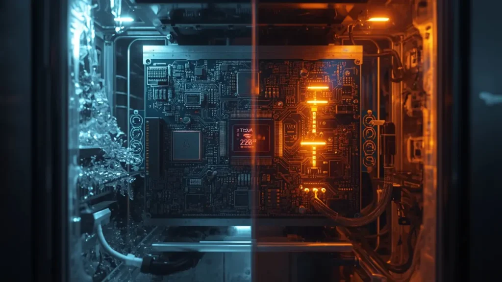
Aerospace PCB Thermal Vacuum (TVAC) Reliability Testing
Every aerospace PCB that leaves our factory carries a pedigree of validation data proving it can survive the journey from launch pad to orbit—or from runway to stratosphere. Aerospace PCB testing is not an afterthought; it is an integrated discipline that begins with material qualification and extends through environmental stress screening, electrical verification, and long-term reliability prediction. At Shenzhen Hongda Circuit Technology, we have structured our test laboratories around the failure modes that actually kill boards in the field: thermal fatigue, vacuum outgassing, vibration-induced solder joint fracture, and latent defects invisible to standard inspection.
Why Is Aerospace PCB Testing Essential for Flight Hardware?
The cost of a field failure in aerospace defies simple calculation. A failed satellite PCB may require a $200 million replacement launch. A defective avionics board in a commercial airliner triggers emergency landings, regulatory investigations, and fleet-wide grounding. These consequences make aerospace PCB reliability testing an investment rather than an expense. Our approach combines IPC-6012 Class 3 acceptance criteria with program-specific test protocols derived from NASA-STD-8739, ECSS-Q-ST-70-11, and MIL-STD-810H.
Common Aerospace PCB Tests and Validation Methods
We organize our test capabilities into five categories that map to the major environmental stresses encountered in aerospace service.
Thermal Vacuum Test (TVAC) for Space-Grade PCBs
The thermal vacuum test PCB protocol simulates the combined effects of space vacuum and orbital thermal cycling. In our TVAC chambers, we achieve vacuum levels below 1×10⁻⁶ mbar—equivalent to LEO orbital pressure—and cycle temperatures between -55°C and +125°C (or wider ranges for deep-space missions). This test reveals outgassing-induced contamination, solder joint creep under thermal load, and delamination at material interfaces. Every space-grade board undergoes thermal vacuum cycles with in-situ electrical monitoring to catch intermittent failures that only appear under combined stress.
Thermal Cycling Test for Aerospace PCB Durability
While TVAC addresses vacuum-specific risks, standalone thermal cycling test PCB protocols isolate the effects of CTE mismatch between laminate, copper, and components. We cycle boards between -65°C and +150°C for 500–1000 cycles, monitoring via resistance changes and microsection analysis. This test is particularly critical for high-layer-count boards where Z-axis expansion can fracture stacked microvias. Our equipment includes high-speed thermal shock chambers with rapid transition rates, accelerating failure mode identification.
Vibration and Mechanical Shock Testing
Launch vehicles impose severe mechanical environments. Our vibration test systems apply random vibration profiles from 20–2000 Hz with power spectral densities up to 0.04 g²/Hz, followed by half-sine shock pulses of 50–100 G. We instrument boards with strain gauges and accelerometers to identify resonant frequencies and stress concentrations. For rigid-flex designs, we add bend-cycle testing—typically 200,000 flex cycles—to validate dynamic flex zone integrity.
Humidity and Environmental Exposure Testing
Even aerospace electronics face humidity during ground handling and tropical launch sites. Our humidity chambers subject boards to 85°C/85% RH conditions for 1000 hours per IPC-TM-650 Method 2.6.14, followed by insulation resistance testing to detect CAF growth and electrochemical migration. For salt-fog exposure relevant to naval aviation, we run MIL-STD-810H Method 509.7 cycles to validate conformal coating integrity.
Electrical Performance and Signal Integrity Verification
Environmental testing means nothing if the board does not meet electrical specifications. Our electrical test suite includes:
- Flying probe testing for 100% netlist verification on prototypes
- TDR (Time Domain Reflectometry) for impedance control validation on RF and high-speed digital lines
- Network analyzer characterization for mmWave aerospace applications
- Hi-pot and insulation resistance testing to verify dielectric withstand
- X-ray inspection (AXI) using Nordson DAGE 3D CT systems for BGA void quantification and hidden solder joint analysis
What Is a Thermal Vacuum Test PCB and When Is It Required?
A thermal vacuum test PCB is a specialized test vehicle or flight article subjected to TVAC conditions to validate design margins. We recommend TVAC testing for:
- All space-grade PCBs (LEO, GEO, deep space)
- High-altitude UAV electronics operating above 50,000 ft
- Scientific instruments with optical or thermal surfaces sensitive to contamination
- Any program requiring NASA, ESA, or MIL-PRF-31032 qualification
Our TVAC test reports document vacuum level, temperature profile, cycle count, electrical performance drift, and post-test visual inspection results—delivering the documentation package that prime contractors need for mission acceptance.
Reliability Verification Process at Shenzhen Hongda Circuit Technology
Our test flow follows a gated structure:
- Incoming Material Qualification: ASTM E595 outgassing, Dk/Df characterization, copper foil adhesion
- Process Validation: First article inspection, microsection analysis, AOI on every inner layer using SCREEN Ledia LDI exposure data
- Environmental Stress Screening (ESS): TVAC, thermal cycling, vibration per program requirements
- Electrical Verification: 100% flying probe or bed-of-nails testing, supplemented by RF characterization
- Final Inspection and Documentation: IPC-A-610 Class 3 workmanship review, COC generation, lot traceability archive
Industry Standards for Aerospace PCB Testing
We maintain compliance with the following standards, selected based on program requirements:
- IPC-6012 Class 3 / IPC-6012DS: Space and military avionics performance specifications
- IPC-J-STD-001 Space Addendum: Space-grade soldering and assembly requirements
- NASA-STD-8739 series: NASA workmanship standards for soldering and cable harnesses
- MIL-STD-810H: Environmental engineering considerations and laboratory tests
- ECSS-Q-ST-70-02C: ESA thermal vacuum outgassing test standard
- AS9100D: Aerospace quality management system underpinning all test activities
Aerospace PCB Design Standards: Guidelines for Reliable Electronic Systems
Designing a printed circuit board for aerospace service is fundamentally different from designing a consumer product. The margin for error is zero, the regulatory scrutiny is intense, and the cost of a redesign can delay a program by months. Aerospace PCB design standards exist not to constrain innovation but to codify decades of hard-won lessons about what fails in flight and why. At Shenzhen Hongda Circuit Technology, our engineering team works within these standards daily—translating IPC, NASA, and military requirements into manufacturable, testable, and certifiable hardware.
Why Are Aerospace PCB Design Standards Critical?
Standards provide a common language between OEMs, Tier-1 suppliers, and PCB fabricators. When a designer specifies IPC-6012 Class 3, both parties understand that copper wicking must not exceed industry limits, plating voids are strictly controlled, and every via must withstand thermal cycling without barrel cracks. This clarity eliminates ambiguity, reduces respins, and accelerates qualification. For procurement teams, standards also create objective criteria for supplier evaluation—if a fabricator cannot demonstrate IPC-6012DS compliance, they are unlikely to deliver flight-worthy hardware.
Common Aerospace PCB Design Standards and Specifications
IPC Standards for Aerospace PCB Fabrication and Assembly
The IPC family forms the backbone of aerospace PCB quality. We build to:
- IPC-2221/2222: Generic and sectional design standards establishing trace width, spacing, and via diameter rules
- IPC-2223: Design standard for flexible and rigid-flex PCBs, critical for modern avionics packaging
- IPC-6012 Class 3 / IPC-6012DS: Performance specification for rigid PCBs with the space addendum adding outgassing and extended thermal cycling requirements
- IPC-6013 Class 3: Qualification for flexible circuits used in aerospace harness replacements
- IPC-A-610 Class 3: Acceptability criteria for electronic assemblies, defining solder joint quality under magnification
- IPC-J-STD-001 Space Addendum: Space addendum for soldering requirements, mandating pre-bake and vacuum-compatible fluxes
Our manufacturing upgrades include SCREEN Ledia laser direct imaging (LDI) systems that achieve fine trace/space geometries, enabling designers to push IPC-2222 density limits while maintaining Class 3 reliability. Our Mitsubishi laser drilling machines achieve fine blind via diameters for high-density aerospace interconnects.
NASA Workmanship Guidelines for Space Electronics
NASA-STD-8739 series documents govern soldering, cable harnessing, and printed wiring board acceptance for NASA programs. Key requirements include:
- NASA-STD-8739.3: Soldering of electrical connections, specifying wetting angles, fillet geometry, and thermal profile control
- NASA-STD-8739.4: Crimping, interconnecting cables, harnesses, and wiring—relevant for rigid-flex transitions
- NASA-STD-8739.5: Fiber optic cable termination and testing
We train our technicians to NASA workmanship standards and maintain certification records for every operator handling flight hardware.
Military Standards for Defense Aerospace PCBs
Defense programs add layers of performance and traceability requirements:
- MIL-PRF-31032: Performance specification for printed circuit boards, requiring QPL-listed materials, full traceability, and destructive physical analysis (DPA)
- MIL-STD-810H: Environmental test methods defining temperature, humidity, vibration, and shock profiles
- MIL-STD-461: EMI/EMC requirements ensuring boards do not emit or are immune to electromagnetic interference in combat environments
Our facility maintains the documentation and process controls necessary for MIL-PRF-31032 qualification, including XRF copper purity verification and Dk/Df characterization.
Company-Specific Design Rules and OEM Requirements
Major aerospace OEMs—Boeing, Airbus, Lockheed Martin, Northrop Grumman—impose company-specific design rules that supplement industry standards. These may include unique via fill requirements, restricted material lists, or proprietary stackup architectures. We engage with OEM engineering teams during the proposal phase to capture these requirements and embed them into our manufacturing instructions.
Key PCB Design Considerations for Aerospace Applications
Layer Stackup and Impedance Control
Aerospace PCBs frequently combine multiple layers with mixed signal types: RF, high-speed digital, power, and control. Our stackup design services use field solvers (HFSS, CST) to optimize layer assignments, minimizing crosstalk and ensuring impedance tolerance within target specs. We support advanced HDI stackups with microvias, saving routing area compared to traditional through-hole designs. Our interlayer alignment precision reaches fine tolerance levels for mass production and prototype builds.
Signal Integrity for High-Speed Aerospace Interconnects
Modern avionics process sensor data, video streams, and communication protocols at multi-gigabit speeds. We guide designers on:
- Differential pair routing with strict length matching
- Via stub reduction through backdrilling or blind via structures
- Power integrity analysis to minimize ground bounce and simultaneous switching noise
- Material selection for low-loss transmission using ultra-low-loss CCL
Thermal Design and Heat Dissipation in Vacuum
Space electronics cannot rely on convection cooling. We design thermal vias, copper coin inlays, and heavy copper planes to conduct heat to radiative surfaces. Our thermal modeling predicts junction temperatures under worst-case solar exposure and eclipse conditions.
EMI/EMC Shielding and Containment
Aerospace platforms pack sensitive receivers alongside high-power transmitters. We implement:
- Ground plane stitching via arrays to control EMI
- Shielded via fences around RF sections
- Controlled impedance transitions to minimize reflections
- Conformal coating and encapsulation for additional isolation
Reliability Margin and Derating
Military and space programs require component derating—operating capacitors, resistors, and semiconductors well below their maximum ratings. We support derating analysis by providing accurate thermal models and recommending board-level cooling strategies that maintain junction temperatures within derated limits.
Design Documentation Requirements for Aerospace Programs
Complete documentation packages reduce program risk and accelerate audits. We provide:
- Fabrication drawings with material callouts, stackup details, and impedance targets
- Gerber, drill, and pick-and-place files in industry-standard formats
- Test point maps and probe access diagrams
- Microsection photographs showing plating quality and via structure
- SPC data demonstrating process capability (Cpk>1.67)
- Non-conformance and corrective action logs
Best Practices for Aerospace PCB Design Success
- Engage your fabricator early: Stackup and material decisions made at the schematic stage prevent costly respins later.
- Design for test: Include test pads and probe access for 100% electrical verification.
- Model the environment: Simulate thermal, vibration, and radiation conditions in the design phase.
- Plan for obsolescence: Select materials and components with long procurement horizons.
- Maintain configuration control: Track every design revision with ECO documentation.
Space Grade PCB: High-Reliability Circuit Boards for Satellite and Space Applications
The boundary between Earth and space is unforgiving. Extreme temperature swings, hard vacuum, ionizing radiation, and launch vibrations—each of these forces conspires to destroy ordinary electronics. A space grade PCB is not merely a robust circuit board; it is a precision-engineered system where every material, every via, and every solder joint is optimized for survival in the most hostile environment humans have ever placed hardware. At Shenzhen Hongda Circuit Technology, we manufacture space-grade printed circuit boards that have powered LEO constellations, geostationary communication platforms, and deep-space scientific instruments.
What Is a Space Grade PCB?
A space grade PCB—also called a space-qualified or flight-proven printed circuit board—meets stringent material, manufacturing, and testing criteria defined by NASA, ESA, and IPC space addenda. Unlike commercial or even standard military-grade boards, space-grade PCBs must demonstrate:
TML ≤1.0 %, CVCM ≤0.1 %
- Thermal cycling survival across -55°C to +125°C (or wider for deep space)
- Radiation tolerance for Total Ionizing Dose (TID) and Single Event Effects (SEE)
- Vibration and shock resistance matching launch vehicle profiles
- Full material and process traceability for mission assurance
Our space-grade production line operates under AS9100D with dedicated cleanroom environments, segregated tooling, and lot-controlled material stocks to prevent cross-contamination with commercial products.
Space Environment Challenges for PCB Electronics
Radiation Effects on Space PCB Materials and Components
Beyond Earth’s magnetosphere, electronics face a constant barrage of protons, heavy ions, and gamma rays. Total Ionizing Dose (TID) gradually degrades semiconductor performance, while Single Event Upsets (SEU) can flip logic states in memory devices. We mitigate radiation risks through:
- Material selection: Polyimide and PTFE substrates exhibit lower radiation-induced conductivity compared to standard FR-4
- Layout techniques: Guard rings around sensitive nodes, triple-modular redundancy for critical signals, and decoupling capacitor networks
- Shielding integration: Tantalum or copper shielding layers embedded in the PCB stackup
Vacuum Environment and Outgassing Risks
(pressure <1 ×10⁻⁶ mbar), materials release volatile compounds that condense onto optical surfaces, thermal radiators, and RF antennas. We validate every space-grade material lot through ASTM E595 testing and pre-bake boards per IPC-1601 to drive out residual moisture. Our adhesiveless polyimide constructions achieve TML below 0.5%—half the NASA limit—providing margin for long-duration missions.
Thermal Cycling in Orbital Environments
Satellites in LEO experience 16 thermal cycles per day as they pass through Earth’s shadow. Over a long-duration mission, that exceeds tens of thousands of cycles. We design boards with matched CTE materials—copper-invar-copper (CIC) cores for large BGAs, low-CTE polyimide for flex sections—and validate via life through accelerated thermal cycling before flight qualification.
Mechanical Stress During Launch and Deployment
Launch vehicle random vibration (20–2000 Hz, 0.04 g²/Hz PSD) and pyrotechnic shock test the mechanical limits of every interconnect. We reinforce mounting holes with plated eyelets, use stiffeners on thin flex sections, and design rigid-flex transitions to eliminate stress concentration points.
Key Features of Space Grade PCBs
High Reliability Through Zero-Defect Manufacturing
Our space-grade line targets extremely low defect rates through:
- 100% automated optical inspection (AOI) on every inner layer using LDI data
- 3D X-ray computed tomography (CT) via Nordson DAGE systems for BGA and hidden joint verification
- Flying probe testing on 100% of nets for prototypes; bed-of-nails for production
- Microsection analysis on every lot to verify plating thickness, via fill quality, and layer registration
Radiation Resistance Design Strategies
We work with radiation effects engineers to implement:
- TID-hardened layouts: Appropriate trace spacing to prevent radiation-induced leakage
- SEE mitigation: Redundant routing, error-correcting memory interfaces, and watchdog circuits
- Prompt dose survivability: High-voltage design margins for transient event scenarios
Thermal Stability Across Extreme Temperature Ranges
Space-grade boards must operate across severe temperature extremes. We select materials with high Tg and use heavy copper for power distribution to minimize resistive heating. Thermal vias and copper coin inlays conduct heat to radiative surfaces coated with high-emissivity black polyimide.
Low Outgassing Materials and Processes
Our space-grade material list includes:
TML<0.5 %, CVCM <0.01%
- Rogers RO3003 (PTFE)
- Isola 370HR (high-Tg FR4, qualified for space)
Typical Space Applications for High-Reliability PCBs
Satellite Communication Systems
LEO and GEO satellites require RF PCBs with stable Dk across temperature for phased-array antennas and transponder modules. We manufacture PTFE-based RF boards with high phase consistency supporting high-frequency communication links.
Spacecraft Avionics and Flight Computers
Flight control computers demand high-layer-count digital boards with HDI microvias for processor-to-memory interconnects. Our HDI technology supports fine-pitch BGAs with signal integrity validated through TDR and VNA measurements.
Deep Space Missions and Planetary Probes
Mars rovers and outer-planet probes face extended radiation exposure and extreme cold. We design boards with extended temperature ranges and radiation-hardened component footprints. Our qualification process includes low-temperature electrical testing to verify performance at cryogenic conditions.
Material Selection for Space Grade PCB Manufacturing
| Material | Tg (°C) | TML (%) | CVCM (%) | Best For |
|---|---|---|---|---|
| Polyimide (Pyralux) | >200 | 0.3 | 0.03 | Flexible circuits, long-duration LEO |
| PTFE (RO3003) | >280 | 0.2 | 0.02 | RF/microwave, low dielectric loss |
| High-Tg FR4 (370HR) | 180 | 0.8 | 0.08 | Cost-sensitive short missions |
| Ceramic (AlN) | N/A | 0.1 | 0.01 | High-power, thermal management |
Avionics PCB: Reliable Circuit Boards for Modern Aircraft Electronics
Modern aircraft are flying data centers. From fly-by-wire flight controls to satellite communication terminals, avionics PCB technology underpins every critical function in the cockpit, cabin, and airframe. The shift toward electric propulsion, autonomous flight, and connected aviation is accelerating demand for printed circuit boards that deliver higher computing density, lighter weight, and uncompromising reliability in vibration-rich, thermally challenging environments. At Shenzhen Hongda Circuit Technology, we manufacture avionics PCBs that meet DO-254 hardware assurance levels, AS9100D quality systems, and the performance benchmarks set by leading aerospace OEMs.
What Is an Avionics PCB?
An avionics PCB is a specialized printed circuit board designed for airborne electronic systems. These boards must comply with regulatory frameworks including DO-178C (software) and DO-254 (hardware) for Design Assurance Levels (DAL) A through E, depending on the criticality of the function. Unlike industrial or automotive boards, avionics PCBs face:
- Continuous vibration from turbine engines and aerodynamic turbulence
- Rapid temperature changes during climb and descent
- Electromagnetic interference from radar, communication, and navigation transmitters
- Strict weight budgets that reward every gram saved
Our avionics manufacturing line supports these requirements with IPC Class 3 workmanship, controlled impedance modeling, and materials qualified for airborne service.
Types of Avionics PCBs for Aircraft Electronics
Rigid Avionics PCBs for Cockpit and Cabin Systems
Traditional rigid boards remain the workhorse for avionics modules with standard form factors. We produce multilayer rigid PCBs with high-Tg FR4 or polyimide cores for flight displays, engine monitoring units, and in-flight entertainment systems. Our capability includes fine trace/space geometries for mass production and prototype builds using SCREEN Ledia LDI systems.
Rigid-Flex Avionics PCBs for Weight-Critical Applications
The avionics rigid flex PCB category is transforming aircraft wiring. By replacing cable harnesses and connector assemblies with integrated flexible interconnects, rigid-flex boards reduce system weight by 10–30% and eliminate potential failure points. We manufacture multilayer rigid-flex designs with polyimide flex cores and FR4 rigid sections for dynamic and static flex applications.
High-Density Interconnect (HDI) Avionics PCBs
Next-generation flight computers and sensor fusion modules demand HDI technology. Our HDI process supports fine-pitch BGAs, stacked microvias, and blind/buried via structures that pack more functionality into smaller footprints, enabling space savings over conventional designs for AI-enhanced mission systems.
Why Are Rigid-Flex PCBs Used in Avionics Systems?
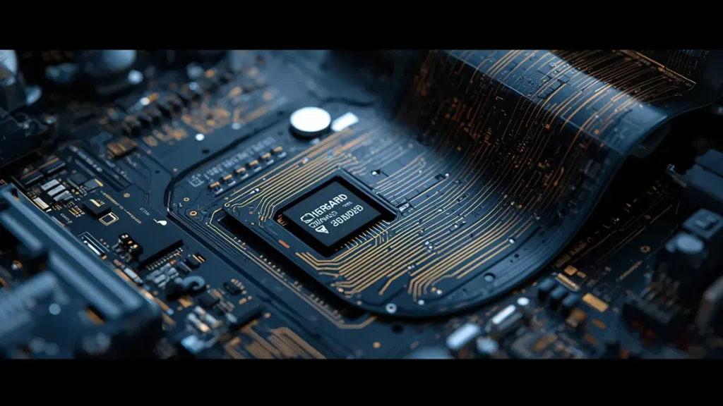
Avionics Rigid-Flex PCB with Bent Polyimide Substrate
The aerospace industry’s adoption of rigid-flex technology is a structural response to key engineering pressures.
Space Saving and Volume Reduction in Airframe Integration
Modern aircraft allocate minimal volume to electronics. Rigid-flex boards fold into tight compartments behind instrument panels, under seats, and within wing structures. A single rigid-flex assembly can replace multiple separate rigid boards and cable harnesses, reducing packaging volume significantly.
Reduced Connector Count and Improved Reliability
Every connector is a potential failure point. Rigid-flex eliminates board-to-board connectors by creating continuous copper paths between rigid sections. This improves mean time between failures (MTBF) and reduces the maintenance burden during aircraft turnaround. For safety-critical flight control systems, this reliability improvement directly supports DAL A certification.
Lightweight Design for Fuel Efficiency
The aviation industry measures weight in grams. A typical rigid-flex avionics assembly saves significant weight compared to an equivalent wired solution. Across a fleet, that translates to measurable fuel savings and reduced carbon emissions—metrics that matter to airlines and regulators alike.
Enhanced Signal Integrity for High-Frequency Avionics
Rigid-flex maintains controlled impedance across the entire interconnect path, eliminating the impedance discontinuities introduced by connectors and cables. For satellite communication systems, this ensures low insertion loss and excellent return loss across the operating bandwidth.
Typical Avionics Applications for High-Reliability PCBs
Flight Control Systems and Fly-by-Wire Electronics
Flight control computers process sensor inputs and command actuator movements with millisecond latency. We manufacture the high-layer-count digital boards that host these processors, with redundancy designed into both the layout and the manufacturing process. Every flight control board undergoes 100% electrical testing and environmental stress screening.
Navigation and GPS Systems
Precision navigation requires RF PCBs with stable phase characteristics. We produce PTFE-based RF boards for GPS receivers, inertial measurement units (IMU), and attitude heading reference systems (AHRS). These boards maintain stable phase consistency at L-band frequencies, ensuring accurate position fixes under dynamic flight conditions.
Communication and Satellite Link Systems
Cockpit voice and data links, SATCOM terminals, and VHF/UHF transceivers demand boards that operate across multiple frequency bands without mutual interference. We implement ground plane segregation, shielded via fences, and controlled impedance transitions to isolate sensitive receivers from high-power transmitters.
Radar and Electronic Warfare Systems
Weather radar, terrain avoidance, and military electronic warfare systems push frequencies into microwave and millimeter-wave bands. Our high-frequency PCB capabilities support these demands with low-loss PTFE substrates and precision-machined cavity structures.
Design Considerations for Avionics PCB Manufacturing
Vibration and Mechanical Robustness
We design boards with reinforced mounting holes, stiffener integration, and strain relief for flex sections. Our vibration testing validates designs against airborne vibration profiles.
Thermal Management in Confined Avionics Bays
Avionics compartments have limited airflow. We use thermal vias, heavy copper planes, and thermally conductive substrates to move heat from components to chassis mounting points. Our thermal modeling predicts junction temperatures under worst-case ambient conditions.
EMI/EMC Compliance for Airborne Certification
DO-160G Section 20 and 21 define conducted and radiated emissions limits. We design with:
- Continuous ground planes with minimal splits
- Decoupling capacitor arrays near high-speed devices
- Controlled rise times to limit harmonic content
- Shielding cans and conductive gaskets where required
Maintainability and Modular Design
Line-replaceable units (LRUs) require boards that can be swapped quickly in the field. We design with standardized connectors, polarization keys, and labeling that supports rapid identification and replacement.
Frequently Asked Questions for Aerospace PCB Buyers: Supplier Selection Guide
When procurement professionals and supply chain managers search for aerospace PCB manufacturers, they need more than a price quote—they need confidence that a supplier can deliver mission-critical hardware on time, on budget, and to specification.
What Certifications Should I Verify Before Qualifying an Aerospace PCB Supplier?
Certifications are the primary filter for aerospace PCB supplier selection. At minimum, a credible supplier must hold:
AS9100D: The aerospace quality management system standard that builds on ISO 9001 with additional requirements for risk management, traceability, and supplier control. Without AS9100D, most aerospace OEMs and Tier-1 contractors will not engage.
IPC-6012 Class 3 or Class 3/A (IPC-6012DS): The performance specification for rigid PCBs. Class 3 is the highest general reliability class; Class 3/A (or IPC-6012DS space addendum) adds space-specific outgassing and extended thermal cycling requirements.
IPC-A-610 Class 3: Defines acceptability criteria for electronic assemblies, ensuring solder joint quality under magnification.
MIL-PRF-31032: Required for military programs, adding QPL-listed materials, destructive physical analysis (DPA), and full traceability.
NASA-STD-8739 series: Governs soldering and workmanship for NASA missions.
At Shenzhen Hongda Circuit Technology, we maintain AS9100D certification, build to IPC-6012 Class 3/3A (IPC-6012DS), and support military programs with full material traceability and long-term record retention. We provide certification documentation upfront during the RFQ phase, eliminating qualification delays.
How Can I Assess a Supplier’s Manufacturing Capability for Complex Aerospace PCBs?
Manufacturing capability assessment goes beyond browsing a website. Buyers should request:
Capability matrix: Verify layer count range (we support 4–28 layers for standard mass production, and higher layer counts for custom builds), minimum trace/space (1.8 mil/1.8 mil mass production standard), microvia capabilities, and material portfolio (polyimide, PTFE, ceramic).
Equipment list: Look for modern technology including SCREEN Ledia laser direct imaging (LDI) for fine traces, automated optical inspection (AOI) with 3D capability, Nordson DAGE X-ray CT for hidden joint verification, and flying probe testers for 100% electrical verification.
Process capability data: Cpk >1.67 impedance tolerance and plating thickness.
Reference programs: Request case studies or customer references from similar aerospace applications.
Our Shenzhen facility operates advanced laminate processing, HDI production, and sequential lamination with precise interlayer alignment. We publish our capability matrix and invite virtual factory tours for qualified buyers.
How Do Suppliers Handle Material Traceability and Documentation for Aerospace Programs?
Traceability is non-negotiable in aerospace. A qualified supplier must provide:
Lot-level material tracking: Every laminate roll, copper foil batch, prepreg lot, and solder paste jar logged with certificate of conformance (COC).
Manufacturing data package (MDP): Gerber files, drill files, stackup details, impedance test data, microsection photographs, and SPC charts.
Test reports: TVAC, thermal cycling, vibration, electrical test, and X-ray inspection results per program requirements.
Non-conformance and corrective action logs: Documented evidence of how defects were identified, contained, and resolved.
Long-term record retention: Standards such as MIL-PRF-31032 and AS9100D require records to be maintained for 10–15+ years.
Our ERP system tracks hundreds of parameters per batch, from raw material receipt through final shipment. Buyers receive a complete documentation package with every delivery, formatted for customer quality audits and regulatory inspections.
What Support Should I Expect During Design-for-Manufacturability (DFM) and Early Engagement?
The best aerospace PCB suppliers act as engineering partners, not just fabricators. Early engagement should include:
Pre-layout stackup consultation: Material selection, impedance modeling, and layer assignment before routing begins.
DFM analysis: Detailed reports identifying manufacturability risks such as insufficient annular rings, problematic via aspect ratios, or solder mask coverage gaps.
Design for test (DFT) review: Ensuring probe access, test point placement, and boundary scan compatibility.
Signal integrity support: TDR validation, network analyzer characterization, and simulation model provision for high-speed designs.
Prototype-to-production scaling: Process optimization to maintain yield and performance as volumes increase.
At Shenzhen Hongda Circuit Technology, we assign a dedicated applications engineer to every aerospace program from RFQ through first article. This single point of contact coordinates DFM reviews, material qualification, test planning, and documentation—reducing communication overhead and accelerating time-to-market.
From Design to Orbit with Shenzhen Hongda Circuit Technology
The aerospace PCB industry sits at the intersection of materials science, electrical engineering, and mission assurance. Whether your program requires the extreme reliability of polyimide for deep-space probes, the RF precision of PTFE for satellite communications, the thermal conductivity of ceramic for high-power avionics, or the weight-saving elegance of rigid-flex for next-generation aircraft, the fundamentals remain constant: traceable materials, validated processes, rigorous testing, and complete documentation.
At Shenzhen Hongda Circuit Technology Co., Ltd., we have invested in the equipment, certifications, and engineering expertise to translate these fundamentals into flight-proven hardware. Our SCREEN Ledia LDI systems, Mitsubishi laser drilling platforms, Lauffer lamination systems, and Nordson DAGE X-ray CT scanners represent state-of-the-art capability in PCB manufacturing. Our AS9100D quality system, IPC-6012 Class 3/3A (IPC-6012DS) compliance, and MIL-PRF-31032 process controls provide the audit trail that aerospace programs demand.
But equipment and certifications are only the foundation. What distinguishes a true aerospace partner is the willingness to engage early, challenge assumptions, and share risk. From the first DFM review through the final TVAC test report, our engineering team works alongside your designers and reliability engineers to ensure that every board that leaves our factory is ready for the mission it was built to serve.
When failure is not an option, choose a partner that treats every board as if it were riding the next rocket. Contact Shenzhen Hongda Circuit Technology Co., Ltd. to discuss your next aerospace PCB program.
About Author
David Chen https://www.linkedin.com/in/pcbcoming
David Chen boasts an extensive professional background in PCBA manufacturing, PCBA testing, and PCBA optimization, with specialized expertise in high-precision PCBA fault analysis and rigorous PCBA reliability testing. The author has worked with high-layer-count server PCB fabrication, ultra-low-loss backplane stackups, and thermo-mechanical reliability optimization for AI infrastructure projects involving 112G and 224G PAM4 architectures. Skilled in complex circuit design and cutting-edge advanced PCB manufacturing processes, he delivers solutions that elevate product durability and performance across industrial applications. His technical articles focusing on PCBA manufacturing workflows and testing methodologies are widely cited by industry peers, research institutions, and technical platforms, solidifying his reputation as a recognized technical authority in the global circuit board manufacturing sector.