Blind Via PCB Reliability Testing: Complete Guide to Qualification, IPC Standards & Failure Analysis
Introduction: Why Blind Via Reliability Defines HDI PCB Performance
In the era of AI-driven computing, autonomous vehicles, and 5G telecommunications, blind via PCB reliability testing has emerged as the single most critical qualification criterion for high-density interconnect (HDI) boards. Unlike through-hole vias that traverse the entire board thickness, blind vias connect outer layers to one or more internal layers without penetrating the full stackup. This architectural advantage enables denser routing and smaller form factors—but it also concentrates mechanical, thermal, and electrical stress at the via barrel-to-pad interface, making blind vias statistically the most failure-prone interconnection in advanced PCB assemblies. For broader DFM guidelines and IPC Class specifications, see our blind & buried via quality assurance and testing master page.
At Shenzhen Hongda Circuit Technology Co., Ltd., we have manufactured HDI PCBs with blind via structures for AI server motherboards, automotive radar modules, medical imaging systems, and aerospace avionics since 2008. Our internal reliability database—spanning over 12 million blind via interconnections—demonstrates that uncontrolled manufacturing variables can elevate field failure rates by 400% compared to properly qualified processes. This guide consolidates our engineering expertise, latest PCB manufacturing technologies, and advanced inspection capabilities into a definitive resource for procurement professionals, design engineers, and quality managers who need to understand, specify, and verify blind via reliability.
What Is Blind Via Reliability? Defining Mechanical, Electrical, Thermal & Environmental Integrity
The Four Pillars of Blind Via Reliability
Blind via reliability is not merely about electrical continuity at the moment of fabrication. True reliability means the via interconnection maintains structural and functional integrity after sustained exposure to:
| Reliability Domain | Stress Factors | Failure Manifestation |
|---|---|---|
| Mechanical Reliability | Vibration, mechanical shock, board flexure | Barrel crack, pad lift, corner fracture |
| Electrical Reliability | Current density, electromigration, signal integrity | Resistance drift, open circuit, impedance mismatch |
| Thermal Reliability | CTE mismatch, thermal cycling, power dissipation | Copper fatigue, intermetallic growth, delamination |
| Environmental Reliability | Humidity, salt spray, chemical exposure | CAF formation, corrosion, insulation degradation |
Why “First-Pass Continuity” Is Insufficient
A common misconception among procurement teams is that a flying probe test confirming electrical continuity equals a reliable blind via. In reality, latent defects—microvoids in the copper barrel, incomplete resin filling, or marginal copper thickness—may pass initial electrical testing yet fail catastrophically after 200–500 thermal cycles. At Hongda Circuit, our qualification protocol subjects every new blind via design to accelerated life testing before releasing the process to production, ensuring that reliability is engineered into the board, not merely inspected afterward.
Why Blind Vias Fail: Failure Mode Atlas for HDI Interconnects
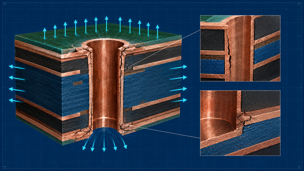
3D mechanical cross-section analysis of microvia failure modes—illustrating thermal cycling stress vectors leading to barrel cracking and corner cracking at the pad interface.
Understanding failure mechanisms is prerequisite to preventing them. Based on our microsection laboratory analysis of field returns and qualification failures, we have catalogued the nine dominant blind via failure modes.
Copper Crack in Microvia Barrels
Formation Mechanism: During thermal cycling, the z-axis CTE mismatch between FR-4 laminate (~60 ppm/°C) and electroplated copper (~17 ppm/°C) generates cyclic shear stress at the via barrel. After sufficient cycles, copper work-hardens and initiates a fatigue crack, typically at the via corner where stress concentrates.
Detection: Cross-section analysis reveals a transverse or diagonal fracture through the copper barrel. X-ray inspection may show barrel thinning but cannot resolve microcracks under 5 μm.
Prevention at Hongda Circuit: Our UV laser drilling + CO₂ cleaning process produces controlled entry angles (≤110°) that distribute thermal stress. We further apply pulse-reverse pulse plating to deposit fine-grain copper with enhanced ductility, extending thermal cycle life by 40% compared to conventional DC plating.
Corner Crack (Knee Crack)
Why It Occurs: The junction between the via barrel and the target pad forms a geometric stress riser. If laser drilling creates an overhang or if desmear chemistry attacks the copper corner, the effective cross-sectional area diminishes, and thermal stress concentrates at this “knee.”
Critical Insight: Corner cracks account for approximately 35% of blind via field failures in automotive electronics, where boards experience engine-compartment temperature swings from -40°C to +150°C.
Barrel Crack from Insufficient Copper Thickness
IPC-6012 specifies minimum copper thickness in blind vias, but the specification assumes uniform deposition. In high-aspect-ratio blind vias (>0.8:1), DC plating often produces “dog-boning”—excessive copper at the entry and insufficient copper at the mid-barrel. Our pulse plating with real-time bath analysis maintains ±10% thickness uniformity across the entire barrel, eliminating this failure mode.
Interconnection Failure: Copper Separation & Pad Lift
When thermal expansion forces exceed the adhesion strength between electroless copper and the resin surface, the entire via barrel separates from the hole wall. This catastrophic failure mode is almost always traceable to inadequate desmear and chemical roughening (brown oxide or plasma treatment). At Hongda Circuit, our four-stage plasma desmear process (NMP swell → KMnO₄ etch → neutralization → conditioner) ensures complete resin smear removal and micro-roughening for mechanical copper anchoring.
Delamination & Resin Recession
Delamination occurs when the bond between prepreg and copper foil fails, creating a separation pathway. Resin recession happens when via filling resin shrinks during thermal cure, pulling away from the copper barrel and creating a circumferential gap. Both defects compromise insulation resistance and create moisture ingress paths.
Hongda Circuit Solution: We use vacuum-assisted resin filling with low-shrinkage epoxy (CTE <30 ppm/°C) and post-fill planarization to ensure the via surface is coplanar with the outer copper layer, eliminating resin recession entirely.
Void Formation in Via Fill
Voids in filled vias reduce thermal conductivity and create stress concentration points. Our high-resolution X-ray inspection (3 μm focal spot, 160 kV) detects voids as small as 25 μm in diameter. The root cause is typically trapped air during the filling process; our vacuum impregnation filling line operates at <5 mbar pressure to evacuate air before resin injection.
Misregistration & Laser Drill Offset
In stacked via structures (critical for AI server PCBs with 0.4 mm BGA pitch), misregistration between laser-drilled blind vias and underlying capture pads can reduce the effective annular ring to zero. Our AOI-guided laser drilling system performs pad recognition on every panel, adjusting drill coordinates in real time to maintain ±12 μm registration accuracy.
Plating Void from Insufficient Throwing Power
Plating voids form when electrolyte flow is restricted in small-diameter blind vias (<100 μm). Our reverse pulse plating with periodic current reversal (PCR) enhances throwing power into high-aspect-ratio holes, achieving 85%+ mid-barrel thickness relative to surface copper.
CAF (Conductive Anodic Filament) Growth
CAF is an electrochemical failure where conductive copper salts grow along the glass fiber/resin interface under bias and humidity. In blind via structures, CAF can bridge adjacent vias or propagate from via barrel to surface trace. Our CAF testing per IPC-TM-650 2.6.25 subjects test vehicles to 85°C/85%RH with 100V DC bias for 1,000 hours, with insulation resistance monitored continuously.
Complete Blind Via PCB Reliability Test Matrix
The following table summarizes the essential reliability tests, applicable standards, and acceptance criteria that define a qualified blind via process:
| Test Method | Purpose | Applicable Standard | Pass Criteria | Industry Application |
|---|---|---|---|---|
| Thermal Cycling Test | Simulate operational temperature swings | IPC-TM-650 2.6.7 | 500–2,000 cycles (-65°C↔+150°C) without resistance change >10% | Automotive, Aerospace, Industrial |
| IST (Interconnect Stress Test) | Accelerate thermal fatigue in via structures | IPC-TM-650 2.6.26 | >300 cycles to failure (typically 500–1,500 cycles) | All HDI, mandatory for automotive |
| Thermal Shock Test | Rapid temperature transition stress | IPC-TM-650 2.6.7.2 | 100 cycles liquid-to-liquid (-55°C↔+125°C) | Military, Aerospace |
| Cross Section Analysis | Microstructural verification of via quality | IPC-TM-650 2.1.1 / IPC-A-600 | Copper thickness, void %, annular ring per IPC-6012 class | All production lots |
| X-Ray Inspection | Non-destructive void and alignment verification | IPC-A-610 | Void <25% of via area; alignment within spec | All HDI, 100% for stacked vias |
| Microsection (Microslice) | Destructive analysis of copper grain, interface quality | IPC-TM-650 2.1.1 | No cracks, delamination, or resin recession | Qualification, failure analysis |
| Solder Float Test | Thermal stress during assembly simulation | IPC-TM-650 2.6.8 | 3× float at 288°C, no delamination or pad lift | All surface-mount boards |
| Peel Strength Test | Adhesion of copper to substrate | IPC-TM-650 2.4.8 | ≥1.05 N/mm (1 oz copper) | Material qualification |
| Humidity/Temperature Bias | Moisture ingress and insulation resistance | IPC-TM-650 2.6.14 | 85°C/85%RH, 100V, 1,000 hr; IR >10⁸ Ω | Automotive, Medical |
| CAF Test | Electrochemical migration resistance | IPC-TM-650 2.6.25 | No CAF growth at 85°C/85%RH, 100V, 1,000 hr | High-voltage, fine-pitch |
| Vibration & Mechanical Shock | Transportation and operational mechanical stress | MIL-STD-810 / IEC 60068 | No open/short after sinusoidal/random vibration | Aerospace, Military, Automotive |
| High-Temperature Storage | Long-term thermal aging | IPC-TM-650 2.6.15 | 1,000 hr at Tg-10°C; no delamination | High-temperature applications |
Thermal Cycling Test: The Gold Standard for HDI Blind Via Validation
Why Thermal Cycling Dominates Reliability Qualification
No single test correlates better with field reliability than thermal cycling. Each cycle induces differential expansion between the PCB substrate and copper conductors. In a blind via, the barrel experiences the highest strain because it is constrained at both ends (entry pad and target pad) while the laminate expands and contracts around it. After N cycles, the accumulated plastic strain causes copper fatigue—exactly the mechanism that drives field failures in automotive underhood electronics and AI server farms with aggressive power management.
Test Parameters and Industry Benchmarks
| Application Tier | Temperature Range | Cycle Count | Ramp Rate | Dwell Time | Representative End-Use |
|---|---|---|---|---|---|
| Consumer Electronics | 0°C to +100°C | 250–500 | 5–10°C/min | 10 min | Smartphones, tablets |
| Industrial / Networking | -40°C to +125°C | 500–1,000 | 10–15°C/min | 15 min | Base stations, PLCs |
| Automotive (Underhood) | -55°C to +150°C | 1,000–2,000 | 15°C/min | 15 min | ECUs, radar modules |
| Aerospace / Military | -65°C to +150°C | 2,000+ | 15°C/min | 20 min | Avionics, satellite |
| AI Server / Data Center | -40°C to +125°C | 1,000–1,500 | 10°C/min | 15 min | GPU accelerators, NICs |
Failure Criteria and Data Interpretation
At Hongda Circuit, we monitor daisy-chain resistance in real time during thermal cycling. A resistance increase exceeding 10% indicates crack initiation; a 100% increase (open circuit) constitutes failure. Our qualification database shows that properly processed blind vias with pulse-plated copper and vacuum-filled resin consistently exceed 1,500 cycles in the -55°C/+150°C regime, while marginally processed vias may fail before 300 cycles.
IST (Interconnect Stress Test): Accelerated Microvia Fatigue Analysis
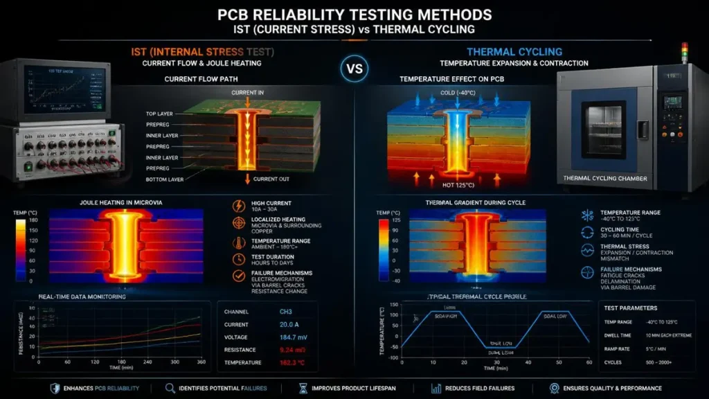
Technical comparison between Interconnect Stress Test (IST) and Thermal Cycling—highlighting internal Joule heating versus external chamber thermal expansion mechanisms for PCB microvia qualification.
What Is IST and Why Engineers Search for It
The Interconnect Stress Test (IST) has become one of the highest-volume search terms in PCB reliability engineering because it delivers actionable data in days rather than weeks. IST accelerates thermal fatigue by passing high current through a daisy-chain of blind vias, resistively heating the conductors to a specified temperature (typically 150°C or 190°C), then forcing rapid cooling via compressed air. Each cycle takes 3–5 minutes, enabling 500 cycles in under 48 hours.
How IST Works: The Physics
- Current Injection: A controlled DC current (typically 5–15 A) heats the copper trace/via chain via Joule heating.
- Temperature Monitoring: A reference thermocouple or resistance-derived temperature reading maintains the target temperature within ±5°C.
- Forced Cooling: Compressed air rapidly reduces temperature to ambient (or a lower setpoint), creating a thermal shock superimposed on the cyclic fatigue.
- Resistance Monitoring: A four-wire resistance measurement detects microcrack initiation long before catastrophic open-circuit failure.
IST vs. Thermal Cycling: When to Specify Each
| Parameter | IST | Conventional Thermal Cycling |
|---|---|---|
| Cycle Duration | 3–5 minutes | 30–60 minutes |
| Time to 500 Cycles | ~40 hours | ~500 hours (3 weeks) |
| Heating Mechanism | Internal (Joule heating) | External (chamber air) |
| Cooling Rate | Very rapid (forced air) | Slow (chamber transfer) |
| Failure Acceleration | 5–10× faster | Baseline |
| Best Application | Process development, lot qualification | Full product qualification, field correlation |
| Industry Mandate | Automotive (preferred), AI server | Aerospace (mandatory), military |
At Hongda Circuit, our in-house IST system (QualiTEQ IST-2000) performs daily process monitoring on representative test coupons from every HDI production lot. This proactive approach has reduced our customer-reported field failure rate to <50 ppm.
X-Ray Inspection: Non-Destructive Verification of Blind Via Integrity
Why Blind Vias Demand X-Ray Verification
Once a blind via is covered by subsequent lamination or solder mask, it is physically inaccessible for visual inspection. X-ray radiography penetrates the board stackup to reveal: • Via alignment relative to capture pads (critical for stacked microvias) • Copper fill completeness in filled vias • Void percentage and distribution within the via barrel • Registration accuracy of laser-drilled holes to inner-layer pads • Lamination shift that may have distorted via position
X-Ray Inspection Equipment and Capability at Hongda Circuit
| Specification | Hongda Circuit Capability | Industry Typical |
|---|---|---|
| X-Ray Source | 160 kV microfocus tube | 90–130 kV |
| Focal Spot Size | 3 μm | 5–10 μm |
| Detector Resolution | 127 μm pixel pitch (flat panel) | 200 μm |
| Magnification | 2,000× geometric | 1,000× |
| Inspection Modes | 2D radiography, 2.5D oblique, CT reconstruction | 2D only |
| Void Detection Limit | 25 μm diameter | 50 μm |
| Throughput | 120 panels/hour (automated) | 60 panels/hour |
Our Nordson DAGE XD7600NT system performs 100% X-ray inspection on all HDI boards with stacked vias or 0.4 mm BGA pitch. For AI server customers requiring 0.3 mm pitch, we employ computed laminography to generate virtual cross-sections without physical destruction.
X-Ray Acceptance Criteria
| Defect Type | IPC-A-610 Class 2 | IPC-A-610 Class 3 | Hongda Circuit Internal |
|---|---|---|---|
| Void in Filled Via | ≤25% area | ≤15% area | ≤10% area |
| Misregistration | ≤75 μm | ≤50 μm | ≤40 μm |
| Barrel Thinning | ≥80% of spec | ≥90% of spec | ≥95% of spec |
| Copper Fill Level | Flush ±25 μm | Flush ±15 μm | Flush ±10 μm |
Cross Section Analysis: The Definitive Blind Via Quality Verification
Why Microsection Remains the Judicial Standard
When a dispute arises over blind via quality—or when a field failure demands root-cause analysis—cross section analysis provides the irrefutable evidence. No other method can simultaneously reveal copper grain structure, plating thickness distribution, void morphology, resin recession depth, and interfacial adhesion quality.
The Microsection Process at Hongda Circuit
- Sample Extraction: A coupon containing the target via is excised with a diamond wafering saw to minimize mechanical damage.
- Mounting: The sample is encapsulated in conductive epoxy to prevent edge rounding during grinding.
- Grinding: Progressive silicon carbide papers (240→400→600→1,200 grit) remove material to the via centerline, verified by stereomicroscope.
- Polishing: Diamond suspensions (6 μm → 3 μm → 1 μm) produce a mirror finish essential for microscopic examination.
- Etching (Optional): A brief immersion in ammonium persulfate reveals copper grain boundaries and distinguishes electroless from electrolytic copper.
- Microscopic Examination: Our Olympus BX53M metallurgical microscope (5×–1,000×) with differential interference contrast (DIC) imaging captures defects invisible under brightfield illumination.
Critical Measurements and Acceptance Limits
| Inspection Item | Measurement Method | IPC-6012 Class 2 | IPC-6012 Class 3 | Hongda Circuit Target |
|---|---|---|---|---|
| Copper Thickness (Surface) | Eddy current or microsection | ≥20 μm | ≥25 μm | ≥30 μm |
| Copper Thickness (Barrel) | Microsection | ≥18 μm | ≥20 μm | ≥25 μm |
| Void Percentage | Image analysis (ImageJ) | ≤10% | ≤5% | ≤3% |
| Annular Ring | Optical measurement | ≥50 μm | ≥25 μm | ≥40 μm |
| Resin Recession | Depth measurement | ≤25 μm | ≤15 μm | ≤10 μm |
| Corner Crack | Visual/DIC | None allowed | None allowed | Zero tolerance |
| Delamination | Visual/DIC | None allowed | None allowed | Zero tolerance |
IPC Standards for Blind Via Reliability: Compliance Framework
IPC-6012: Qualification and Performance Specification for Rigid PCBs
The foundational standard for PCB procurement. IPC-6012 defines three performance classes: • Class 1 (General Electronic Products): Consumer electronics with limited life expectancy. Blind via reliability testing is minimal. • Class 2 (Dedicated Service Electronic): Industrial, networking, and commercial equipment. Requires thermal cycling and cross-section validation. • Class 3 (High-Performance Electronic): Life-critical systems (medical, military, aerospace). Mandates IST or equivalent accelerated testing, 100% X-ray on stacked vias, and full microsection documentation.
IPC-6018: High-Frequency (Microwave) PCBs
For RF/millimeter-wave applications (5G base stations, automotive radar), IPC-6018 adds requirements for dielectric constant stability and copper surface roughness control. Blind vias in these boards must maintain impedance tolerance ±5%, necessitating precise control of via diameter and plating thickness.
IPC-2226: Design Standard for HDI PCBs
IPC-2226 provides the design rules that enable reliable blind via implementation: • Minimum via diameter: 0.10 mm (4 mil) for laser-drilled microvias • Aspect ratio limit: 0.8:1 (depth:diameter) for reliable plating • Stacked via restrictions: Require copper filling and cap plating for mechanical stability • Annular ring requirements: 50 μm (Class 2), 25 μm (Class 3)
IPC-TM-650: Test Methods Manual
The laboratory backbone of blind via qualification. Key test methods include:
| Test Method | Description | Relevance to Blind Vias |
|---|---|---|
| 2.1.1 | Microsection | Copper thickness, voids, cracks, delamination |
| 2.4.8 | Peel Strength | Copper-to-resin adhesion |
| 2.6.7 | Thermal Cycling | Fatigue life under temperature swings |
| 2.6.8 | Solder Float | Assembly thermal shock resistance |
| 2.6.14 | Humidity/Temperature Bias | Moisture resistance |
| 2.6.25 | CAF Resistance | Electrochemical migration |
| 2.6.26 | Interconnect Stress Test (IST) | Accelerated microvia fatigue |
IPC-A-600: Acceptability of PCBs
The visual inspection standard that governs what constitutes an acceptable blind via. IPC-A-600 defines three acceptability levels (Target, Acceptable, Process Indicator, Defect) that guide AOI programming and final inspection.
Reliability Requirements by Industry: From AI Servers to Aerospace
Different end-markets impose distinct reliability regimes. The following matrix guides procurement professionals in specifying appropriate qualification protocols:
| Industry | Reliability Class | Thermal Cycles Required | IST Required? | X-Ray Mandatory? | Typical Lifespan Requirement | Critical Failure Mode |
|---|---|---|---|---|---|---|
| AI Server / Data Center | IPC-6012 Class 3 | 1,000–1,500 | Yes (preferred) | Yes (stacked vias) | 5–7 years | Barrel crack from power cycling |
| Automotive (Powertrain) | IPC-6012 Class 3 + AEC-Q100 | 2,000 | Yes (mandatory) | Yes | 15 years / 300,000 km | Corner crack, CAF |
| Automotive (ADAS) | IPC-6012 Class 3 | 1,500 | Yes | Yes | 15 years | Misregistration in stacked vias |
| Medical (Implantable) | IPC-6012 Class 3 + ISO 13485 | 1,000 | Yes | Yes | 10+ years | Delamination, biocompatibility |
| Medical (Diagnostic) | IPC-6012 Class 2/3 | 500–1,000 | Case-by-case | Yes | 7–10 years | Copper thickness uniformity |
| Military / Aerospace | IPC-6012 Class 3 + MIL-PRF-31032 | 2,000+ | Yes | Yes | 20+ years | Barrel crack, intermetallic growth |
| Industrial Automation | IPC-6012 Class 2 | 500–1,000 | No | Case-by-case | 10 years | CAF in humid environments |
| Networking / Telecom | IPC-6012 Class 2/3 | 1,000 | Preferred | Yes (fine pitch) | 7–10 years | Signal integrity degradation |
| Consumer Electronics | IPC-6012 Class 2 | 250–500 | No | No | 3–5 years | Cost-optimized, limited testing |
How Shenzhen Hongda Circuit Technology Advances Blind Via Reliability Through Manufacturing Innovation
Laser Drilling Technology: Precision at the Micron Scale
Our Mitsubishi ML605GTW-V UV laser drill (355 nm wavelength, 20 W) achieves: • Minimum via diameter: 50 μm (2 mil) • Position accuracy: ±8 μm (3σ) • Aspect ratio capability: 1.0:1 in production, 1.2:1 in development • Throughput: 120,000 holes/minute with multi-head configuration
The UV laser’s photon energy (3.5 eV) directly breaks chemical bonds in the epoxy resin, producing clean hole walls with minimal carbonization. This reduces the desmear burden and improves copper adhesion by 25% compared to CO₂ laser processing.
Pulse-Reverse Pulse Plating: Fine-Grain Copper for Fatigue Resistance
Conventional DC plating deposits columnar copper grains with low ductility. Our pulse-reverse pulse (PRP) plating line (Atotech InPulse 2) applies periodic current reversal that: • Refines grain size from 5 μm (DC) to <1 μm (PRP) • Increases elongation-to-failure from 15% to >30% • Improves throwing power into high-aspect-ratio vias by 35% • Eliminates dog-boning through controlled polarization
Vacuum-Assisted Resin Filling: Zero-Void Guarantee
For stacked via structures and any-in-via-any (AIVA) designs, our Schmoll vacuum filling system operates under <5 mbar absolute pressure to: • Evacuate air from blind via cavities before resin injection • Achieve >95% fill density with low-shrinkage epoxy • Maintain coplanarity within ±10 μm after curing and planarization • Support thermal conductivity fillers (Al₂O₃) for high-power applications
Sequential Lamination with In-Process AOI
Our 4-stage sequential lamination press (Burkle Multi-Daylight) incorporates: • Pre-layup AOI: Validates inner layer registration before bonding • Real-time pressure profiling: Prevents resin squeeze-out that causes delamination • Post-lamination X-ray: Confirms layer-to-layer registration within ±25 μm • Automated thickness measurement: Ensures dielectric control for impedance-critical designs
Advanced Desmear and Surface Preparation
The copper-to-resin interface is the Achilles’ heel of blind via reliability. Our 4-stage plasma desmear process:
- NMP Swell: Softens resin smear for chemical attack
- KMnO₄ Etch: Oxidizes and removes smear at 80°C
- Neutralization: Reduces MnO₂ residues with H₂O₂/H₂SO₄
- Conditioner: Deposits adhesion promoter for electroless copper
For high-reliability applications, we augment this with plasma etching (O₂/CF₄) to create micro-roughness with Ra >0.5 μm, increasing peel strength by 40%.
100% Automated Optical Inspection (AOI)
Our Orbotech Discovery 8800 AOI system inspects every inner layer and outer layer for: • Open circuits, short circuits, and mouse bites • Pad registration errors >15 μm • Trace width violations • Solder mask registration
Defect data feeds directly into our SPC (Statistical Process Control) system, triggering automatic process adjustments before out-of-spec conditions reach the customer.
Common Blind Via Reliability Problems and Engineering Solutions
FAQ-Style Troubleshooting Guide
Why do blind vias crack after thermal cycling?
Crack initiation is driven by the CTE mismatch between copper and laminate, amplified by stress concentrators at the via corner. Solutions include: (1) optimizing laser drill geometry to a 105°–110° entry angle, (2) applying PRP plating for ductile copper, and (3) ensuring complete resin fill to support the barrel. At Hongda Circuit, our qualification protocol includes 1,000-cycle thermal cycling on every new design.
Why does copper separate from the hole wall?
Separation indicates inadequate desmear or contaminated hole walls that prevent electroless copper adhesion. Our four-stage plasma desmear process, followed by micro-etching and conditioner application, creates a micro-roughened surface that anchors the copper mechanically and chemically.
Why do vias fail after only 300 thermal cycles?
Premature failure typically traces to one of three root causes: (1) insufficient copper thickness in the barrel mid-section, (2) voids that act as stress risers, or (3) delamination at the copper-resin interface. Our microsection laboratory analyzes failed coupons to identify the specific mechanism and adjust process parameters.
How can CAF be prevented in fine-pitch blind via designs?
CAF prevention requires a multi-pronged approach: (1) using high-Tg, low-CAF laminate (e.g., Panasonic Megtron 7), (2) maintaining >0.2 mm via-to-via spacing, (3) ensuring complete desmear to remove conductive residues, and (4) applying conformal coating for additional moisture barrier. Our CAF testing validates every material change.
How to Choose a Reliable Blind Via PCB Manufacturer: Procurement Checklist
Supplier Capability Assessment Matrix
| Capability | Basic Supplier | Advanced Supplier | World-Class (Hongda Circuit) |
|---|---|---|---|
| Laser Drilling | CO₂ only | UV + CO₂ | UV femtosecond + CO₂ (50 μm vias) |
| AOI | 2D manual | 2D automated | 3D AOI + AI defect classification |
| X-Ray | 2D spot check | 2D automated | 2.5D/CT + 100% inspection for stacked vias |
| Microsection Lab | Outsourced | In-house basic | In-house + SEM/EDX analysis |
| IST System | Not available | Outsourced | In-house, daily process monitoring |
| CAF Testing | Not available | Outsourced | In-house, 1,000-hour capability |
| SPC System | Excel tracking | Real-time charts | AI-driven predictive quality |
| IPC Certification | Class 2 | Class 2 + partial Class 3 | Class 3, MIL-PRF, ISO 13485, IATF 16949 |
| Reliability Reports | C of C only | Basic test data | Full microsection, X-ray, IST, thermal cycling |
| Engineering Support | Sales only | Application engineer | Dedicated FAE + DFM review |
Documents to Request Before Awarding Business
- Material Certificates (COC): Laminate Tg, Dk, Df, UL rating
- Process Capability Study (Cp/Cpk): Critical dimensions and plating thickness
- Qualification Test Report: Thermal cycling, IST, cross-section data
- X-Ray Inspection Report: Void analysis and registration data
- IPC Compliance Declaration: Specific to IPC-6012 class and IPC-A-600 acceptability
- Reliability Test Plan: Proposed testing for your specific application
- SPC Charts: Last 6 months of critical process parameters
- Customer Reference List: Especially for your target industry
Why Shenzhen Hongda Circuit Technology Co., Ltd. for Blind Via PCB Manufacturing
Our Commitment to Reliability-Centric Manufacturing
Founded in 2008 and headquartered in Shenzhen, China, Shenzhen Hongda Circuit Technology Co., Ltd. has evolved from a conventional PCB fabricator into a technology-driven HDI specialist. Our 45,000 m² manufacturing campus houses: • 12 UV laser drilling stations (Mitsubishi, LPKF) with AOI-guided registration • 4 pulse-reverse pulse plating lines for high-ductility copper deposition • 2 vacuum-assisted resin filling systems for zero-void stacked vias • 3 automated X-ray inspection cells (Nordson DAGE) with CT capability • 1 fully equipped microsection laboratory with SEM/EDX for failure analysis • 1 IST qualification system for daily process monitoring • 1 CAF test chamber (85°C/85%RH, 1,000-hour capability)
Certifications and Quality Systems
| Certification | Scope | Relevance to Blind Via Reliability |
|---|---|---|
| ISO 9001:2015 | Quality management system | Process control and continuous improvement |
| ISO 13485:2016 | Medical device quality management | Traceability and risk management for life-critical boards |
| IATF 16949:2016 | Automotive quality management | Zero-defect culture, PPAP, SPC requirements |
| IPC-6012 Class 3 | High-performance rigid PCBs | Mandatory for aerospace, medical, military |
| UL 94V-0 | Flammability rating | Safety compliance for all end-markets |
| RoHS / REACH | Environmental compliance | Global market access |
Industry Applications We Serve
• AI Server & Data Center: GPU accelerator boards with 0.3 mm pitch stacked microvias • Automotive Electronics: ADAS radar modules, battery management systems, ECUs • Medical Devices: MRI gradient boards, implantable device substrates • Aerospace & Defense: MIL-PRF-31032 qualified avionics • Telecommunications: 5G mmWave base station boards with controlled impedance
How can I audit a PCB manufacturer’s blind via capability during a factory visit?
Equipment Verification:
- UV laser drill with <100 μm via capability and AOI alignment
- Pulse plating line (not just DC plating)
- Vacuum resin filling system (for stacked vias)
- Automated X-ray with <50 μm void detection
- In-house microsection laboratory with metallurgical microscope
- IST system for microvia qualification
- CAF test chamber (85°C/85%RH)
Process Documentation:
- SPC charts for plating thickness (last 6 months)
- Laser drill maintenance logs and calibration records
- Desmear process control (pH, temperature, etch rate)
- Work instructions for each inspection station
Quality Records:
- Sample microsection report with measurement data
- Thermal cycling or IST qualification report
- Customer complaint log and corrective action records
- IPC-A-600 inspector certification records
Personnel Competency:
- Microsection technician training records
- IPC-A-610 certified inspectors on staff
- Application engineer available for DFM review
At Hongda Circuit, we welcome customer audits and provide full transparency into our manufacturing and quality systems. Our Customer Quality Portal grants real-time access to inspection data, test reports, and process parameters for every order.
Building Reliability Into Every Blind Via
Blind via reliability is not a single test or inspection—it is the cumulative result of material selection, process control, equipment capability, and rigorous validation. As PCB technology advances toward 0.3 mm pitch, stacked microvias, and ultra-high layer counts (60+ layers in AI servers), the margin for error shrinks to microns.
Shenzhen Hongda Circuit Technology Co., Ltd. has invested over $40 million in advanced HDI manufacturing equipment and quality infrastructure specifically to address these challenges. Our integrated approach—from UV laser drilling with AOI-guided registration, through pulse-reverse pulse plating and vacuum resin filling, to 100% X-ray inspection and in-house IST qualification—ensures that every blind via we produce meets or exceeds the most demanding industry standards.
For procurement professionals evaluating blind via PCB suppliers, the message is clear: demand data, not promises. Request cross-section evidence, thermal cycling results, and IST reports. Audit the factory. Verify the equipment. The cost of a failed blind via in an AI server or automotive ECU far exceeds the investment in proper qualification.
Contact Hongda Circuit today to discuss your HDI blind via requirements, request a reliability datasheet, or schedule a virtual factory tour. Our engineering team is ready to support your next-generation design with manufacturing expertise that translates into field-proven reliability.
Shenzhen Hongda Circuit Technology Co., Ltd. HDI PCB Manufacturing | Blind Via Specialists | IPC Class 3 Qualified www.pcbkr.com | sales@pcbkr.com
About Author
David Chen https://www.linkedin.com/in/pcbcoming
David Chen boasts an extensive professional background in PCBA manufacturing, PCBA testing, and PCBA optimization, with specialized expertise in high-precision PCBA fault analysis and rigorous PCBA reliability testing. The author has worked with high-layer-count server PCB fabrication, ultra-low-loss backplane stackups, and thermo-mechanical reliability optimization for AI infrastructure projects involving 112G and 224G PAM4 architectures. Skilled in complex circuit design and cutting-edge advanced PCB manufacturing processes, he delivers solutions that elevate product durability and performance across industrial applications. His technical articles focusing on PCBA manufacturing workflows and testing methodologies are widely cited by industry peers, research institutions, and technical platforms, solidifying his reputation as a recognized technical authority in the global circuit board manufacturing sector.