What Is Impedance Control in PCB? A Complete Procurement & Engineering Guide
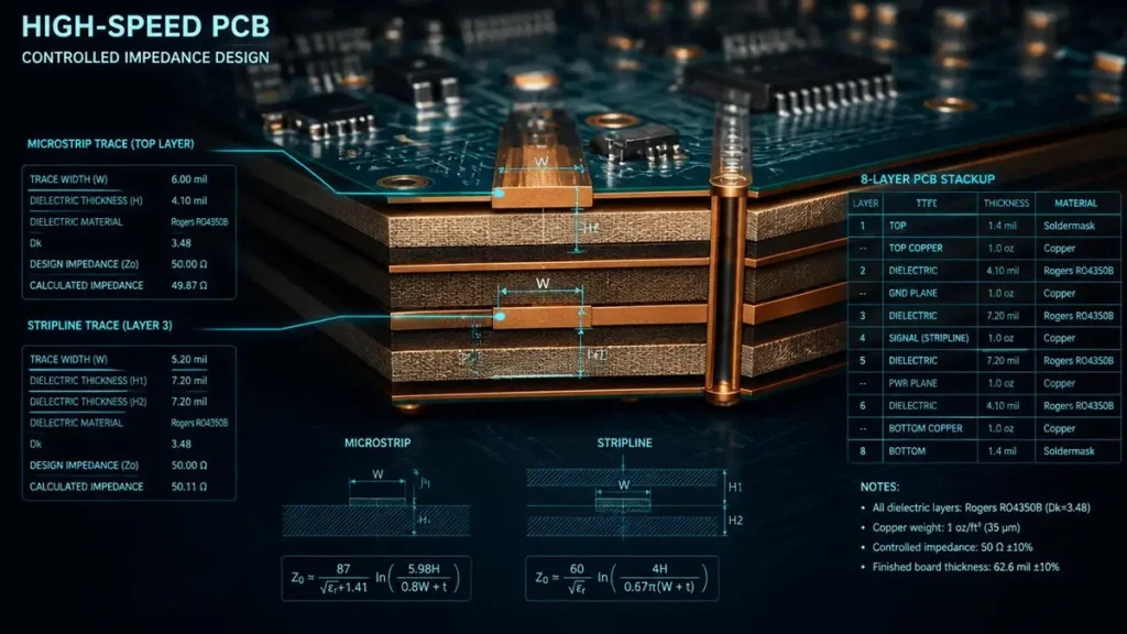
3D Cross-Section of Controlled Impedance PCB Stackup – PCBkr
Introduction: When the Formula Betrays You
Your signal-integrity engineer spent three weeks in Polar Si9000. The stackup checks out: 50 Ω single-ended, 100 Ω differential, Megtron 7 core, everything within ±10 % on paper. You send the RFQ to three factories. The lowest bidder wins. Fourteen weeks later, the 224G PAM4 backplanes arrive, pass DC continuity with flying colors, and die in system-level BER testing by a 4 dB margin. The autopsy? A 3.2 Ω impedance deviation on the differential pairs—well inside the ±10 % tolerance the factory guaranteed, but catastrophic at 56 GHz Nyquist.
This is not a design failure. It is a procurement failure rooted in a misunderstanding of what impedance control actually means in 2026.
What is impedance control in PCB? It is the disciplined practice of governing trace geometry, dielectric thickness, material dielectric constant (Dk), copper properties, and environmental dielectric boundaries so that the characteristic impedance (Z₀) of every critical transmission line remains locked within a predefined, traceable tolerance band throughout the fabrication process.
What is a controlled impedance PCB? It is a board manufactured under process windows tight enough to guarantee that specific signal paths—whether a 50 Ω single-ended microstrip or a 100 Ω differential stripline—meet their electrical specification with documented evidence, typically verified by 100 % TDR (Time Domain Reflectometry) testing on production-specific coupons. A standard PCB only promises continuity. A controlled impedance PCB promises electrical behavior.
At Shenzhen Hongda Circuit Technology Co., Ltd., we shipped over 18,000 panels of controlled impedance boards in the first half of 2026, spanning automotive Ethernet at ±8 % tolerance to AI-server 224G PAM4 channels at ±1.5 %. This guide is written for procurement professionals and design engineers who need to move beyond textbook definitions and understand what it actually takes to manufacture reliable impedance in the era of 112G and 224G signaling.
Why Impedance Control Matters: From Reflection Physics to the 2026 Threshold Collapse
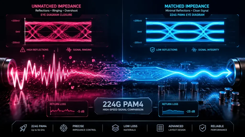
224G PAM4 Signal Integrity & Impedance Control Comparison
The Foundation: Reflection, Overshoot, and EMI
Before we talk about 224G, we need to revisit why impedance control existed in the first place. When a high-speed signal encounters an impedance discontinuity—where the trace width necks down, a via stub changes the reference plane, or a connector footprint mismatches the board—the laws of physics do not negotiate. A portion of the electromagnetic energy reflects back toward the source instead of propagating forward. The reflection coefficient Γ is governed by the simple but unforgiving formula:
Γ = (Z₂ − Z₁) / (Z₂ + Z₁)
Where Z₁ is the incident impedance and Z₂ is the discontinuity impedance. At a 10 % mismatch (55 Ω vs. 50 Ω), Γ = 0.048. That sounds small until you realize that at 56 Gbps PAM4, even this modest reflection creates inter-symbol interference that closes the eye diagram. The reflected wave also interferes with the incident wave at the driver, producing voltage overshoot that can exceed receiver absolute maximum ratings and undershoot that causes false triggering.
Then there is EMI. An impedance mismatch does not just reflect energy internally; it turns the PCB trace into an unintended antenna. The radiated emissions scale with the square of the current discontinuity, which is why uncontrolled impedance boards often fail EMC chamber testing even when the schematic is perfect. For procurement teams sourcing boards for automotive or medical applications, an EMC failure is not a schedule slip—it is a program-killing event.
The 2026 Threshold Collapse: Why ±10 % Is Now a Liability
For decades, the industry treated impedance control as a specialty requirement for RF boards or multi-gigabit serial links. That rule no longer holds. Three forces have collapsed the threshold in 2026.
First, PCIe Gen 6 at 64 GT/s and 224G PAM4 interfaces push Nyquist frequencies beyond 50 GHz. At these speeds, any trace longer than roughly one-tenth of the signal rise-time wavelength behaves as a transmission line, not a lumped conductor. A 2 % impedance mismatch generates reflections that equalization cannot recover.
Second, AI server backplanes now route 112G–224G lanes across 800 mm or more. Every via stub, trace neck, and glass-weave crossing becomes a measurable discontinuity that accumulates along the channel. The cumulative return-loss budget for a 224G link is often less than –18 dB at 56 GHz; there is simply no room for sloppy impedance.
Third, automotive Ethernet and ADAS camera links have moved from convenience features to safety-critical paths. A bit error in a 10GBASE-T1 lane during autonomous emergency braking is not a dropped packet—it is a liability event that can trigger regulatory recalls.
The result is a compression of acceptable tolerance bands that most procurement specifications have not caught up with. Legacy ±10 % was adequate for DDR3 and 1 Gbps Ethernet. In 2026, PCIe Gen 6 and 224G PAM4 demand ±3 % to ±5 %, and our most aggressive AI customers now specify ±1.5 % on differential pairs with 100 Ω nominal. A supplier who quotes ±10 % for a 224G program is not offering a conservative tolerance; they are admitting they do not own the process physics.
At Hongda Circuit, our production data from Q1 and Q2 2026 tells the story clearly. When we process 224G backplanes with full trapezoidal compensation, mSAP etching, and AI-driven etch-parameter control, first-pass impedance yield exceeds 97 %. When we run the same stackup without closed-loop compensation—simulating what a commodity factory does—yield drops to 71 %. The 26 % gap is pure scrap cost and schedule risk.
Key Factors & The Invisible Variables That Kill Impedance
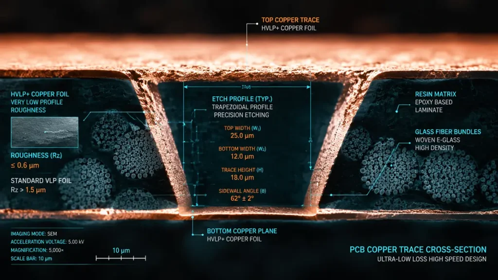
SEM Cross-Section of PCB Copper Trace & Etch Profile
The Five Foundational Elements
Every controlled impedance specification starts with five physical parameters that the designer can influence and the fabricator must control.
Trace width and spacing (W/S) set the primary electromagnetic field geometry. Wider traces lower impedance; tighter differential spacing lowers differential impedance. This is the variable most designers obsess over, but it is only the beginning.
Dielectric thickness (H)—the distance from the trace to its reference plane—has a nearly linear relationship with impedance. A 10 % reduction in H drops single-ended impedance by roughly 7–9 %, depending on the aspect ratio. Thickness control therefore demands sub-mil precision in lamination.
Dielectric constant (Dk) determines how much the electric field couples into the substrate material. At 224G frequencies, Dk is not a single number; it is a frequency-dependent curve. Megtron 7, for example, has Dk ≈ 3.34 at 1 GHz but drops to approximately 3.22 at 56 GHz. Using the wrong Dk value in your field solver introduces systematic error before the first panel enters the factory.
Copper thickness (T) affects both DC resistance and, more importantly, the trace aspect ratio that governs etch behavior. A 1 oz (35 μm) copper layer etches very differently than a half-ounce (18 μm) layer, and the resulting trapezoidal profile changes the effective top width.
Solder mask (Solder Mask) is the fifth element that too many specifications ignore. Liquid photo-imageable (LPI) solder mask has a dielectric constant of approximately 3.5–4.2 at 1 GHz and a thickness of 10–20 μm. When it covers an outer-layer microstrip, it increases the effective Dk surrounding the trace and drops impedance by a measurable amount. We will return to this in the topology section, but for now, treat solder mask as a dielectric boundary that must be modeled, not ignored.
Invisible Killer 1: Trapezoidal Etch Compensation
Chemical etching is isotropic. The etchant attacks copper laterally as well as vertically, which means the finished trace is trapezoidal, not rectangular. On a 1 oz outer layer, the top width can be 0.8–1.2 mil narrower than the base width per side. If your field solver assumes a perfect rectangle, the actual impedance will be 3–5 Ω higher than predicted. At 224G, that is a channel-killing error.
At Shenzhen Hongda Circuit, we do not accept this as inevitable. Our process engineering team models etch factor per copper weight, layer type, and etchant chemistry, then pre-compensates the photoplot artwork before imaging. Inner-layer cores and outer layers run on isolated process lines to prevent cross-contamination of etch parameters. Since Q1 2026, Line 7 has operated under an AI-driven closed-loop system fed by inline eddy-current copper-thickness probes at 0.1 μm resolution. The system adjusts etchant spray pressure, temperature, and conveyor speed in real time. Between March and May 2026, this raised impedance Cpk from 1.18 to 1.61, with trace-width sigma dropping from 2.8 μm to 1.4 μm. That is the difference between a board that passes TDR and a board that passes system-level SI qualification.
Invisible Killer 2: Fiber Weave Effect
Standard FR-4 and high-speed laminates use woven glass fiber bundles with Dk ≈ 6.0 embedded in resin with Dk ≈ 3.0. When a 75 μm trace happens to run directly over a glass bundle, its local Dk spikes. When it crosses a resin-rich pocket, Dk drops. Over a 300 mm differential pair, this “weave effect” creates localized impedance swings of ±4 Ω—enough to violate a ±3 % window even if the average impedance is perfect.
The procurement countermeasure is not to hope for luck. It is to specify spread-glass or flat-glass prepreg (Panasonic Megtron 7 with flat-glass construction is our default for 224G programs) and to require the fabricator to rotate the panel image 10°–15° relative to the glass weave during stackup planning. At Hongda, our stackup engineering team runs weave-mapping simulations before committing to production. We have seen too many 112G programs fail glass-weave skew testing because the designer specified standard 1080 glass and left the rotation angle to chance.
Invisible Killer 3: Copper Foil Roughness
At 56 GHz, skin depth in copper is approximately 0.28 μm. Standard rolled-annealed copper with surface roughness Rz of 3.5–6 μm has topography 12–21× greater than the skin depth. The current does not flow through the peaks and valleys; it flows around them, effectively lengthening the path and increasing both resistance and inductance. The result is an additional 2.8–3.5 dB/100 mm of conductor loss that no FFE or DFE equalizer can recover, and a subtle shift in effective impedance that field solvers rarely model accurately.
The solution is ultra-low-profile (HVLP+) copper foil with Rz ≤ 0.3 μm. At Hongda Circuit, we verify every incoming copper lot on a Keyence VK-X3000 laser confocal profilometer and reject material with Cpk below 1.33. For 224G builds, we mandate JX Nippon or Fukuda HVLP+ foil and archive the profilometry report with the job traveler. If your supplier cannot show you a copper-roughness Cpk chart by lot number, they are not manufacturing 224G-grade boards. They are assembling them and hoping.
Impedance Topologies, Transmission Modes, and the Solder Mask Trap
Single-Ended vs. Differential: Where the Fields Live
Single-ended signaling references impedance to a single ground plane, typically targeting 50 Ω. It is simpler to route and test, but it is vulnerable to ground-bounce noise and requires a clean, low-inductance return path. Differential pairs carry complementary signals and reference each other, with common targets of 85 Ω, 90 Ω, or 100 Ω depending on the interface standard. Differential topology rejects common-mode noise beautifully, but it demands precise intra-pair length matching and tightly coupled spacing—both of which are manufacturing challenges at 3 mil line/space and below.
Microstrip vs. Stripline: The Procurement Trade-Off
Microstrip places the trace on an outer layer with a single reference plane beneath it. It is easier to inspect, easier to rework, and cheaper to process because it avoids buried-layer registration complexity. The downside is EMI radiation into free space and vulnerability to environmental factors like humidity, dust, and—critically—solder mask.
Stripline sandwiches the trace between two reference planes. It offers superior shielding, cleaner signal integrity, and immunity to external dielectric changes. The cost is tighter layer-to-layer registration, more complex stackup symmetry, and typically higher fabrication cost due to additional lamination cycles.
For procurement teams, the decision usually comes down to speed and risk tolerance. Below 10 Gbps, a well-compensated microstrip is acceptable if you understand the solder-mask penalty. Above 25 Gbps, stripline is the safer engineering default, and at 224G it is effectively mandatory for long channels.
The Solder Mask Impedance Killer on Outer Layers
Here is a detail that rarely appears in standard datasheets but costs programs millions in respins. Applying LPI solder mask over an outer-layer microstrip increases the effective Dk surrounding the trace from approximately 3.5 to 4.0–4.2, because the solder mask itself has Dk ≈ 3.5–4.0 at 1 GHz and a thickness of 10–20 μm. The electromagnetic field, which previously saw mostly air (Dk ≈ 1) and substrate, now sees a continuous medium of higher Dk. The result is an impedance drop of 2–8 Ω on the same physical geometry—enough to push a carefully simulated 50 Ω target down to 44 Ω.
A qualified controlled impedance PCB manufacturer must dynamically compensate for this in the pre-production simulation. At Hongda Circuit, our Polar Si9000 material library includes solder-mask Dk values measured at 1, 5, 10, and 28 GHz for every LPI chemistry we qualify. When a customer specifies outer-layer impedance control, we automatically back-calculate the artwork width to absorb the solder-mask delta, then validate the compensated geometry with TDR coupons before production release. If your supplier treats solder mask as an afterthought, your outer-layer impedance targets are wishes, not specifications.
When Do You Need a Controlled Impedance PCB? The Data-Rate Decision Matrix
| Application Segment | Data Rate / Edge Rate | Impedance Tolerance | Typical Material | Procurement Context |
|---|---|---|---|---|
| Consumer / Industrial IoT | < 1 Gbps, > 1 ns rise | ±10 % | Standard FR-4 | Cost-sensitive; prevents ringing on long traces |
| Automotive Ethernet, 5G Sub-6 | 1–10 Gbps | ±8 % | Mid-loss FR-4, Megtron 6 | ADAS and telematics reliability; AEC-Q200 context |
| AI Servers, PCIe Gen 5, 112G PAM4 | 25–56 Gbps | ±5 % | Low-loss Megtron 6/7, Isola I-Tera MT40 | Eye diagram margin; BER targets < 10⁻¹² |
| 224G PAM4 Backplanes, HPC Interconnects | 112–224 Gbps | ±1.5 %–±3 % | Ultra-low-loss Megtron 7/8, Rogers, Taconic | Return loss < –18 dB at 56 GHz; COM margin > 3 dB |
Procurement takeaway: If your BOM includes 224G or PCIe Gen 6 lanes, do not treat ±3 % tolerance as a negotiation point. It is a physics boundary. Specify the tolerance band, the test method (IPC-TM-650 2.5.5.12), and the coupon placement (minimum 3 per panel for IPC Class 3, 5 for aerospace) in your fabrication drawing before you request quotes. A supplier who offers ±10 % for a 224G program is either uninformed or unconcerned about your yield.
From Design to Manufacturing: The Controlled Impedance Engineering Workflow
Stackup Planning with Field Solvers
The first step in any controlled impedance PCB project is a rigorous stackup simulation using a 2D field solver. Classical closed-form formulas (IPC-2141, Wadell) provide estimates within 5–15 %, which was acceptable when tolerance was ±10 % and frequency was 1 GHz. They are dangerously inadequate for 224G. They miss trapezoidal etch, solder-mask loading, frequency-dependent Dk dispersion, and copper roughness correction.
At Hongda Circuit, we use Polar Si9000 with fabricator-specific material databases correlated against measured TDR data from prior production lots. This correlation database—spanning over 4,200 unique stackup configurations—is what allows us to hit ±1.5 % on 224G differential pairs without trial-and-error respins. When a customer sends us preliminary Gerbers, our DFM team does not just check for manufacturability; we run a full impedance pre-simulation and flag any nets where the geometry, material, or layer assignment will not support the stated tolerance.
What we need from your procurement package to do this right:
- Layer sequence and any preferred or qualified materials
- Target impedance values per layer, separated by single-ended and differential
- Tolerance bands and the data-rate context driving them
- Any special requirements: backdrill depth, VIPPO, mSAP, sequential lamination
mSAP vs. Subtractive Etch: Why the Old Process Hits a Wall
Traditional subtractive etch cannot reliably hold ±5 % impedance on trace widths below 3 mil (75 μm). The isotropic undercut becomes too large a percentage of the total width, and the resulting trapezoidal profile introduces unmodeled loss that no post-fabrication tuning can fix. For 224G PAM4, fine-line HDI, and any design with 20 μm line/space, mSAP is no longer a premium option. It is a manufacturing requirement.
Modified Semi-Additive Process (mSAP) starts with an ultra-thin copper seed layer of 2–3 μm. The trace geometry is selectively plated to full height, and a gentle flash etch removes the remaining seed without significantly attacking the plated trace. The result is a near-rectangular profile with undercut below 5 %, compared to 20–25 % undercut in subtractive processing. The impedance predictability improves dramatically, and insertion loss drops because the current path is no longer forced around severe trapezoidal corners.
Hongda Circuit qualified mSAP on 18 μm copper in Q1 2026. Our first production runs achieved trace-width Cpk of 1.45 at 75 μm nominal, with measured insertion-loss improvement of 0.48 dB/100 mm versus subtractive etch on identical Megtron 7 stackups. The capital investment for a full mSAP line exceeds 80 million RMB with 12-plus months equipment lead time. At our Shenzhen facility, mSAP is an integral process, not an outsourced step. When you audit a supplier for 224G work, ask to see their mSAP line in operation. If they subcontract it, they do not control the impedance.
TDR Testing and Impedance Coupon Design: Proof by Measurement
Impedance control is not proven by simulation. It is proven by measurement on every panel that ships. The industry-standard method is TDR (Time Domain Reflectometry) per IPC-TM-650 2.5.5.7 and 2.5.5.12. A fast-rise step generator launches a pulse into a test coupon, and the reflected energy is measured over time. Discontinuities appear as impedance steps on the waveform. Gating isolates the region of interest, and the average impedance within the gate is compared against the target.
Our standard coupon design at Hongda includes:
- 50 Ω single-ended microstrip and stripline reference structures
- 100 Ω and 85 Ω differential pair structures with precise intra-pair coupling
- Length-matched traces for repeatable TDR gating windows
- GSG and GSGSG launch pads compatible with standard differential probes
Every production panel is 100 % TDR tested before shipment. Test results—including measured versus target impedance, waveform plots with gating markers, Cpk statistics by coupon type, and lot traceability—are compiled into a formal impedance test report. For aerospace and medical programs, we retain these records for the full product lifecycle per AS9100D and ISO 13485 requirements. If your supplier offers “sample TDR” or “spot-check TDR,” they are not running a controlled impedance process. They are running a lottery.
Frequently Asked Questions: Controlled Impedance PCB Procurement
What Is the Difference Between a Standard PCB and a Controlled Impedance PCB?
A standard PCB is manufactured to electrical continuity, dimensional, and cosmetic specifications. The fabricator measures whether the traces connect the right pads and whether the board meets IPC-A-600 acceptability criteria. They do not measure, guarantee, or document characteristic impedance. If the impedance happens to be 45 Ω or 65 Ω, that is not their concern.
A controlled impedance PCB requires the manufacturer to simulate the stackup, compensate for trapezoidal etch and solder-mask effects, control dielectric thickness within tight windows, and verify every production panel with TDR coupons. The procurement document must therefore include target Z₀ values, tolerance bands, test-coupon design approval, and formal acceptance criteria—none of which are necessary for a standard board. The price delta is typically 15–35 % depending on tolerance and layer count, but the cost of a respin on a 14-week lead-time program dwarfs that premium.
Why Is Trapezoidal Trace Shape Important for Controlled Impedance PCBs?
Because chemical etching is isotropic, the finished trace is trapeoidal, not rectangular. The top width is narrower than the base width by 0.5–1.0 mil per side on 1 oz copper. A field solver that assumes a perfect rectangle will predict an impedance that is 3–5 Ω lower than reality. At 224G, that error alone can consume your entire channel margin.
To verify that your supplier handles this, ask three questions. First, do they apply etch-compensated artwork based on actual etch-factor data, or do they use raw Gerber width? Second, do they separate inner and outer layer processing to prevent etch-parameter cross-contamination? Third, can they show you etch-factor Cpk data by copper weight and layer type? A qualified supplier will have this documentation. A commodity factory will change the subject.
How Do I Specify Controlled Impedance Requirements on Fabrication Drawings?
Include a dedicated impedance table in your fabrication notes. For each controlled layer, list: layer number, trace type (single-ended or differential), target impedance in ohms, nominal trace width and spacing, tolerance band, and reference planes. Attach a stackup drawing showing dielectric thicknesses, copper weights, and qualified material callouts with manufacturer and grade.
State the test method explicitly: IPC-TM-650 2.5.5.12 for TDR measurement. Specify coupon placement (3 per panel minimum for IPC Class 3, 5 for aerospace or automotive safety). Define the report format: measured impedance, waveform plots, Cpk by coupon, and lot traceability. If you are unsure how to structure this, send your preliminary Gerbers to sales@pcbkr.com. Our DFM team will return a fabrication-notes template tailored to your design within 24 hours.
What Equipment and Certifications Should I Verify for 224G PAM4 Controlled Impedance Manufacturing?
Look for six things. First, in-house mSAP or SAP capability—subtractive etch cannot hold the geometry. Second, laser direct imaging (LDI) such as SCREEN Ledia for fine-line patterning without phototool distortion. Third, laser drilling (Mitsubishi UV/CO₂) for microvia precision that supports tight layer transitions. Fourth, inline copper-thickness monitoring at sub-micron resolution. Fifth, TDR equipment calibrated to IPC standards with traceable certificates. Sixth, material traceability for ultra-low-loss laminates and HVLP+ copper foil with lot-specific profilometry.
Certifications should include ISO 9001, IPC-6012 Class 3 or 3A, and AS9100D for aerospace-grade traceability. At Shenzhen Hongda Circuit, we maintain all of the above at our Shenzhen facility and welcome customer audits by appointment.
How Does Solder Mask Affect Controlled Impedance on Outer Layers?
Solder mask increases the effective dielectric constant surrounding an outer-layer microstrip trace, which drops impedance by 2–8 Ω depending on mask thickness, Dk, and trace geometry. This does not mean you must avoid outer-layer impedance traces, but you must specify that the fabricator include solder-mask Dk in the field-solver simulation and compensate the artwork accordingly.
If your design demands extremely tight tolerance—±3 % or better—the more robust procurement choice is to move critical nets to internal stripline layers. This eliminates the solder-mask variable entirely, along with humidity absorption and mechanical damage risks. At Hongda, we routinely advise customers to migrate 224G differential pairs to stripline unless the form factor absolutely prohibits it. The 0.3 dB insertion-loss penalty of an additional via transition is usually smaller than the impedance uncertainty of an outer-layer microstrip at these tolerances.
Conclusion: Impedance Control Is Manufactured, Not Just Designed
If there is one message to take from this guide, it is that impedance control is not a checkbox you tick in your CAD constraint manager. It is a manufacturing outcome built from three inseparable pillars: material science (low-Dk laminates, HVLP+ copper, flat-glass prepreg), process precision (mSAP etching, AI-driven trapezoidal compensation, solder-mask modeling), and verification discipline (100 % TDR testing, design-specific coupons, Cpk tracking by lot).
At Shenzhen Hongda Circuit Technology Co., Ltd., we have invested over $12 million in dedicated high-speed manufacturing infrastructure—from SCREEN Ledia LDI and Mitsubishi laser drilling to Nordson DAGE X-Ray and Keyence confocal profilometry—to deliver controlled impedance PCBs that meet the demands of 224G PAM4, PCIe Gen 6, and aerospace-grade programs. Our engineering team provides pre-production DFM reviews, stackup optimization, and qualification test planning to ensure your design performs on specification: on cycle one, and on cycle one thousand.
For a structured framework on evaluating PCB suppliers beyond impedance—covering quality systems, financial stability, and supply-chain risk—see our PCB Procurement & Supplier Assessment Guide. If you are ready to dive into the stackup mathematics yourself, our PCB Stackup Impedance Calculator Tutorial walks through Polar Si9000 correlation methods using real production data from our Megtron 7 and Megtron 8 process libraries.
Ready to eliminate impedance surprises from your next program?
Submit your Gerber files, stackup requirements, and impedance specifications to sales@pcbkr.com. Our engineering team will return a complimentary DFM review, impedance simulation report, and detailed quotation within 30 minutes.
Company: Shenzhen Hongda Circuit Technology Co., Ltd.
Website: www.pcbkr.com
Email: sales@pcbkr.com | pcb@pcbkr.com
Phone: +86 0755 23720053
Address: Room 1608-1610, Research Development Comprehensive Building, Baoyunda Logistics Center, Baoan, Shenzhen, China
Unified Social Credit Code: 91440300MA5F6CA091
Certifications: ISO 9001:2026 | AS9100D | IPC-6012 Class 3/3A | ISO 13485 | IATF 16949 | UL
About Author
David Chen https://www.linkedin.com/in/pcbcoming
David Chen boasts an extensive professional background in PCBA manufacturing, PCBA testing, and PCBA optimization, with specialized expertise in high-precision PCBA fault analysis and rigorous PCBA reliability testing. The author has worked with high-layer-count server PCB fabrication, ultra-low-loss backplane stackups, and thermo-mechanical reliability optimization for AI infrastructure projects involving 112G and 224G PAM4 architectures. Skilled in complex circuit design and cutting-edge advanced PCB manufacturing processes, he delivers solutions that elevate product durability and performance across industrial applications. His technical articles focusing on PCBA manufacturing workflows and testing methodologies are widely cited by industry peers, research institutions, and technical platforms, solidifying his reputation as a recognized technical authority in the global circuit board manufacturing sector.