High-Performance SMD LED PCBs for 3535, Cree XPE/XPG/XTE, and High-Power Applications
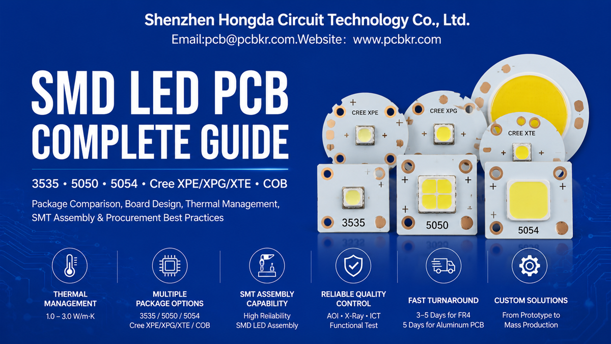
When you’re sourcing SMD LED PCB assemblies for commercial lighting, display modules, or automotive applications, the gap between a functional board and a reliable one comes down to three things: thermal design precision, solder joint integrity, and optical consistency. At Shenzhen Hongda Circuit Technology (PCBKR), we manufacture 3535 LED PCB, Cree XPE LED PCB, Cree XPG LED PCB, and 5050 LED PCB assemblies using aluminum and FR4 substrates with thermal conductivity ranging from 1.0 to 3.0 W/m·K. Our SMT lines handle everything from compact 3535 display arrays to high-power COB modules, with prototype turnaround in 3–5 days for standard FR4 and 5 days for aluminum-backed boards.
Whether you’re building RGB atmosphere lighting for automotive interiors, high-bay industrial fixtures, or fine-pitch LED display panels, the wrong SMD LED circuit board choice will cost you in field failures, color shifts, and rejected batches. This guide breaks down the procurement decisions that actually matter—package selection, pad design rules, reflow profiling, and supplier capability verification—so you can specify boards that perform consistently at volume.
SMD LED Package Comparison: 3535 vs 5050 vs 5054 vs Cree XPE/XPG/XTE vs COB
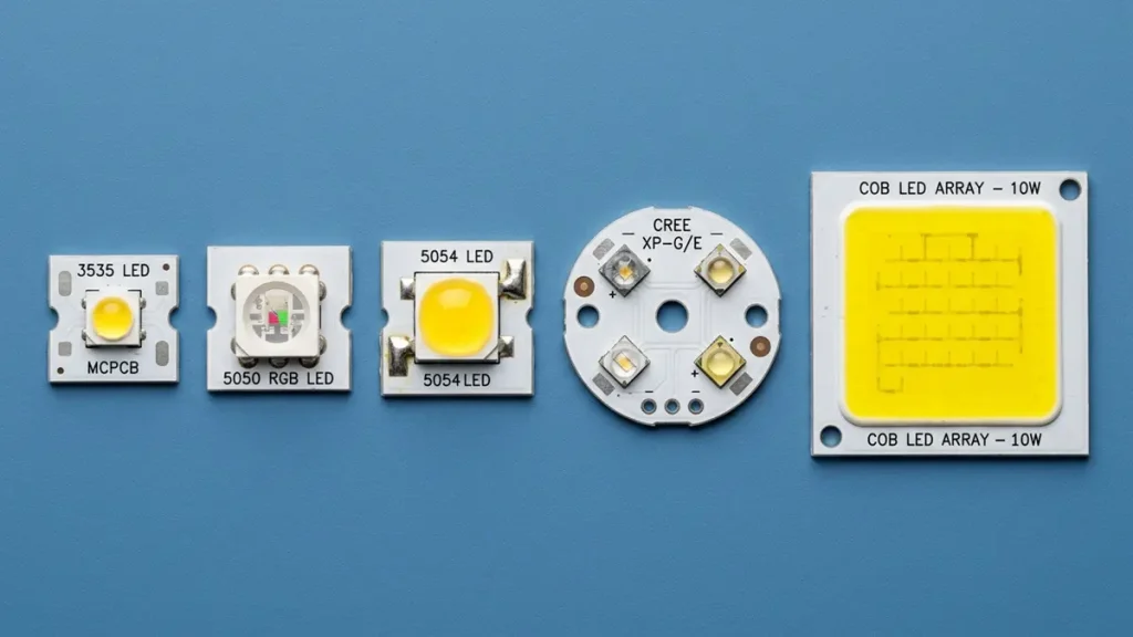
SMD LED Package Comparison: 3535 vs 5050 RGB vs 5054 vs Cree XP-G vs COB Array
Not all LED module PCB platforms are interchangeable. Each package imposes different thermal, electrical, and optical constraints on your board design. Here’s how the major options stack up for production-scale applications.
3535 LED PCB: The Compact Workhorse for Displays and 1W–3W Lighting
The 3535 package (3.5 mm × 3.5 mm, with 3.2 mm × 3.5 mm variants also common) dominates high-density LED display manufacturing. Single-chip configurations handle 0.2W–3W, with standard drive currents at 350 mA–700 mA. The compact footprint allows tight pixel pitches (P2.5–P10), but that density creates thermal bottlenecks if your SMD LED PCB pad design doesn’t account for heat extraction.
For display applications, we typically specify aluminum substrates at 1.5–2.0 mm thickness with 2 oz copper. For general lighting arrays, FR4 with thermal vias can work below 1W per chip, but aluminum MCPCB becomes non-negotiable above 1.5W. The central thermal pad on 3535 LEDs must measure approximately 2.8 mm × 2.8 mm and connect directly to the substrate’s metal core or a dense via array. Oversized pads cause component drift during reflow; undersized pads trap heat and accelerate lumen depreciation.
Cree XPE/XPG/XTE LED PCB: Premium High-Power Chips for Demanding Environments
Cree (now Wolfspeed) XPE, XPG, and XTE series set the benchmark for high-power CREE LED PCB applications. These 3.45 mm × 3.45 mm packages deliver 1W–10W+ per emitter, with drive currents from 700 mA up to 1500 mA for XPG3 variants. Luminous efficacy exceeds 150 lm/W across the XPE and XPG families, but that efficiency depends entirely on your board’s ability to keep junction temperatures below 100°C.
The critical design rule for any Cree XPE LED PCB or Cree XPG LED PCB: follow the manufacturer’s pad geometry exactly. Cree specifies independent anode/cathode pads plus a central thermal pad. The thermal pad must interface directly with the aluminum substrate dielectric layer or connect through at least four 0.3 mm thermal vias to inner copper planes. XPG runs hotter than XPE—pin-compatible electrically, but thermally more demanding. If you’re evaluating whether Cree XPG replace XPE PCB designs without board modifications, the answer is conditional: electrical connections match, but you’ll need higher thermal conductivity dielectric (2.0–3.0 W/m·K) and enhanced copper weight to handle the increased power density.
5050 LED PCB: RGB Tri-Chip Solutions for Commercial and Decorative Lighting
The 5050 LED PCB platform uses a 5.0 mm × 5.0 mm package integrating red, green, and blue chips with a six-pin configuration. Full-white operation draws approximately 60 mA total (20 mA per channel) at 0.5W–3W combined output. RGB SMD LED PCB assembly demands isolated copper channels for each color to prevent electrical crosstalk and thermal stacking. The central thermal pad requires 4.5 mm × 4.5 mm clearance, with separate solder mask openings for each chip’s electrical pads.
For LED strip and signage manufacturers, 5050 remains the default choice because of its excellent color-mixing performance. However, the three-chip architecture generates localized hot spots. Without symmetric trace routing and adequate thermal dissipation, you’ll see color drift across the array within the first 1,000 hours of operation.
5054 LED PCB: Higher Power in a Similar Footprint
At 5.0 mm × 5.4 mm, the 5054 LED PCB package occupies nearly the same board area as 5050 but supports 1W–5W single-chip or dual-chip parallel configurations. The 15% larger pad area improves heat spreading, making 5054 preferable for downlights, track lighting, and outdoor signage where 5050 would run at its thermal limit. Do not reuse 5050 pad layouts for 5054 LEDs—the extended body requires recalculated copper areas and stencil apertures to avoid solder bridging or insufficient fillet formation.
COB LED PCB: Maximum Lumen Density for Industrial Lighting
COB LED PCB assemblies eliminate individual packages by bonding multiple LED chips directly to the substrate. Power ranges from 10W to 500W+, with exceptionally low thermal resistance because the chip sits directly on the board. The trade-off is repairability: a single chip failure usually means replacing the entire module.
COB boards demand mirror-finish aluminum or high-reflectivity white solder mask to maximize light extraction. The bonding area must maintain flatness below 0.05 mm, and dam-and-fill encapsulation requires precise epoxy height control. For 150W+ high-bay or street-light applications, we specify 3.0 W/m·K aluminum substrates with 4 oz copper or direct-bonded copper (DBC) ceramic for UV-curing and industrial vision systems.
| Package | Dimensions | Power Range | Best Application | Thermal Demand | Recommended Substrate | Drive Current |
|---|---|---|---|---|---|---|
| 3535 | 3.5×3.5 mm | 0.2–3W | LED displays / General lighting | Medium | FR4 / Aluminum | 350–700 mA |
| Cree XPE | 3.45×3.45 mm | 1–3W | Automotive / Machine vision | Very High | Aluminum | 700 mA |
| Cree XPG | 3.45×3.45 mm | 3–5W | Premium lighting / Headlamps | Very High | Aluminum / Ceramic | 1000–1500 mA |
| 5050 RGB | 5.0×5.0 mm | 0.5–3W | LED strips / Signage | Medium-High | FR4 / Aluminum | 60 mA/channel |
| 5054 | 5.0×5.4 mm | 1–5W | Commercial high-power lighting | High | Aluminum | 350–700 mA |
| COB | Custom | 10–500W+ | Industrial / Studio lighting | Very High | Aluminum / Mirror Al | Integrated drive |
Substrate Specifications and Thermal Management for SMD LED Circuit Boards
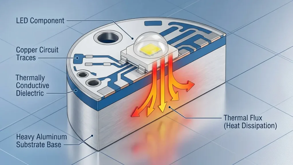
Cross-Sectional Thermal Structure of an Aluminum MCPCB for SMD LED
Your substrate choice determines whether your LED assembly survives 50,000 hours or fails within 12 months. For SMD LED PCB assembly procurement, substrate selection should follow power class, not just unit cost.
Aluminum MCPCB vs FR4 vs High-Thermal FR4
Standard FR4 offers thermal conductivity of 0.3–0.4 W/m·K, sufficient for indicator LEDs and low-power decorative lighting below 1W. Once you cross into 1W–3W territory—typical for 3535 LED PCB board wholesale orders and commercial downlights—aluminum MCPCB becomes essential. Our standard aluminum 5052 substrates deliver 1.0, 2.0, and 3.0 W/m·K thermal conductivity, with operating temperatures up to 150°C.
For mid-power arrays where FR4 is preferred for cost or mechanical flexibility, high-thermal FR4 (1.0–2.0 W/m·K) bridges the gap. However, for Cree XPG automotive headlamps or 150W+ COB street lights, aluminum at 2.0–3.0 W/m·K or ceramic DBC substrates are the only viable options. We also source custom 5.0 W/m·K ceramic-filled aluminum for extreme thermal loads, though this adds approximately 7 days to prototype lead time due to material qualification requirements.
| Substrate Type | Thermal Conductivity | Max Temp | Typical Use | Power Range | Relative Cost |
|---|---|---|---|---|---|
| Aluminum 5052 | 1.0–3.0 W/m·K | ≤150°C | High-power lighting, automotive | 1W–3W+ | Medium |
| Standard FR4 | 0.3–0.4 W/m·K | ≤130°C | Indicators, decorative lighting | <1W | Low |
| High-Thermal FR4 | 1.0–2.0 W/m·K | ≤150°C | Mid-power arrays, industrial | 1W–2W | Medium-High |
Copper Weight, Board Thickness, and Fine-Line Capability
Copper thickness directly impacts current capacity and heat spreading. For SMD LED circuit board designs:
- 0.5–1 oz copper: Standard for low-current indicator applications
- 2 oz copper: Recommended for 5050 RGB arrays and 3W 3535 assemblies
- 3–4 oz copper: Required for Cree XPG and COB modules handling 3W+ per emitter
Board thickness ranges from 0.8 mm to 3.0 mm, with 1.0 mm, 1.5 mm, and 2.0 mm being standard for aluminum LED boards. Our LDI (Laser Direct Imaging) process achieves 3 mil (0.075 mm) minimum line width and spacing for high-density display applications, with 2.5 mil capability available for ultra-fine-pitch LED modules after DFM review.
Surface Finish and Solder Mask Selection
For SMD LED PCB assembly, immersion gold remains the default surface finish. It provides excellent oxidation resistance, flat pad geometry for fine-pitch components, and reliable solder wetting. OSP works for cost-sensitive, short-storage applications. HASL is generally avoided for precision SMD LED work because surface unevenness causes coplanarity issues during reflow.
Solder mask color carries optical implications. White solder mask delivers 85%+ reflectivity, boosting system lumen output by 10–15%—critical for backlight and lighting applications. Black solder mask maximizes display contrast for LED screen modules. Green, blue, and red masks are available for custom branding or indicator differentiation.
SMD LED PCB Pad Design: Engineering the Interface Between Chip and Board
Pad design errors are the leading cause of LED assembly failures in production. A SMD LED PCB pad design that works for one package often fails for another, even when dimensions appear similar.
Thermal Pad Sizing and Copper Connection
The thermal pad must cover at least 85% of the LED’s bottom metal area to conduct heat efficiently. For 3535 LEDs, we specify 2.8 mm × 2.8 mm thermal pads tied to the aluminum substrate or connected through thermal vias. For 5050 and 5054 packages, the thermal pad expands to 4.5 mm × 4.5 mm with corner electrical pads isolated from the central heat slug.
Cree packages demand strict adherence to datasheet dimensions. The XPG3 thermal pad, for example, measures 2.3 mm × 2.3 mm. Enlarging this pad to match generic 3535 layouts causes LED drift during reflow; shrinking it restricts heat flow and elevates junction temperature. Our DFM review cross-checks every custom pad layout against Cree’s official drawings before tooling.
Stencil Aperture and Solder Mask Strategies
Solder mask openings must exceed copper pad dimensions by 0.05–0.1 mm to prevent mask encroachment on wetting surfaces. For stencil design:
- 3535/5050 thermal pads: Use cross-hatch or grid-pattern apertures rather than full openings. This reduces solder paste volume, preventing LED flotation and skewing during reflow. We typically set apertures at 50–70% of pad area for thermal pads, with 0.12–0.15 mm stencil thickness.
- Cree XPE/XPG: Thermal pad apertures at 50–70% of pad area, electrical pads at 90–95% to minimize solder balling.
- Electrical pads: Reduce aperture 5–10% below pad size to control paste volume and prevent bridging.
Stencil printing angle of 45°–60° ensures complete pad coverage, particularly for high-density 3535 LED PCB arrays where missing paste translates directly to open joints.
Trace Routing for Multi-LED Arrays
A single 5050 RGB LED draws approximately 60 mA at full white. A 100-LED parallel array pulls 6A—enough to create significant voltage drop and thermal rise in undersized traces. At 1 oz copper, 6A requires 6 mm trace width for <10°C temperature rise; at 2 oz copper, 3 mm suffices. We route LED power traces at 45° angles or with curved corners to reduce current concentration and EMI. For RGB SMD LED PCB assembly, R/G/B channel spacing must exceed 0.3 mm to prevent optical crosstalk and capacitive coupling.
Advanced Reflow Soldering Process: How to Solder SMD LED on PCB at Production Scale

High-Precision SMT Pick-and-Place Assembly Line for SMD LED PCBs
If you’re researching how to solder SMD LED on PCB assemblies reliably, the critical factor is thermal control. LED packages are more thermally sensitive than standard passive components. Exceeding the SMD LED PCB reflow profile limits by even 10°C can yellow phosphor coatings, shift color temperature by 200K+, or fracture internal bond wires.
PCBKR’s SMT Assembly Workflow
Our SMD LED PCB assembly process follows a controlled five-stage protocol:
1. Solder Paste Printing We use SAC305 or SAC405 no-lead solder paste with Type 4 powder (particle size 20–38 μm) for apertures below 0.4 mm. The 45°–60° squeegee angle ensures 100% pad coverage. For 2835 and 3535 LEDs, we verify paste height and volume using 3D SPI before any component touches the board.
2. SPI Inspection 3D solder paste inspection catches insufficient volume, bridging, and offset before placement. This step alone eliminates 70% of reflow defects that would otherwise require rework.
3. High-Speed Placement Yamaha YSM20R pick-and-place machines deliver ±0.035 mm placement accuracy, critical for fine-pitch LED arrays. We use soft silicone nozzles specifically for LED packages to prevent surface scratching on 3535, 5050, and Cree optics. The machine handles components from 01005 chip resistors up to 50 mm × 50 mm COB modules.
4. Nitrogen Reflow Soldering Our 8-zone nitrogen reflow oven maintains oxygen levels below 500 ppm, minimizing oxide formation on solder joints. The nitrogen atmosphere produces shinier, more reliable fillets with reduced voiding compared to air reflow.
5. 3D AOI Verification Post-reflow, 3D AOI inspects every joint for offset, bridging, insufficient solder, and coplanarity. For Cree four-pad packages, we measure solder height and volume to verify thermal pad wetting. No board ships without 100% optical inspection.
Optimized Temperature Profiles by Package Type
Different LED packages tolerate different thermal limits:
| Zone | 3535/5050/5054 | Cree XPE/XPG/XTE | COB Modules |
|---|---|---|---|
| Preheat (RT–150°C) | 60–90 sec, 1.5–2.5°C/s | 60–90 sec, 1.5–2.0°C/s | 90–120 sec, 1.0–1.5°C/s |
| Soak (150–180°C) | 60–90 sec | 60–90 sec | 90–120 sec |
| Reflow (>217°C) | 60–90 sec TAL | 60–90 sec TAL | 60–90 sec TAL |
| Peak | 245–250°C | 240–245°C | <240°C |
| Peak Duration | <10 sec | <10 sec | <10 sec |
| Cooling | 2–4°C/s | 2–4°C/s | 2–4°C/s |
Aluminum substrates require slower preheat ramps (1.5°C/s max) to prevent thermal warping from CTE mismatch between the metal core and copper traces. Every production run begins with a test board fitted with thermocouples to validate the profile against the specific LED manufacturer’s datasheet.
Common Reflow Defects and Prevention
- Tombstoning: Caused by uneven pad heating or asymmetric paste volume. Prevention: symmetric stencil design, balanced oven zone temperatures, thermal pad-centered packages.
- LED Skewing: Results from excessive paste on thermal pads causing flotation. Prevention: grid-pattern stencil apertures, controlled paste volume at 50–70% of pad area.
- Cold Joints: Peak temperature too low or TAL insufficient. Prevention: thermocouple-verified profiles, nitrogen atmosphere improving wetting at lower temperatures.
- Solder Balls: Paste oxidation or oversized apertures. Prevention: nitrogen reflow, electrical pad apertures 5–10% undersized.
- Color Shift: Phosphor thermal degradation from peaks >260°C. Prevention: package-specific profiles, strict peak enforcement.
Optical Performance, Beam Angle, and Color Consistency
Brightness specifications from LED datasheets assume ideal thermal conditions. Real-world performance on your SMD LED circuit board depends on how well the board manages heat and current distribution.
Luminous Flux and Efficacy by Package
| Package | Typical Flux | Efficacy | Notes |
|---|---|---|---|
| 3535 | 20–50 lm (@0.5W) | 100–130 lm/W | Single-chip, display-optimized |
| 5050 RGB | 60–80 lm (full white) | 80–100 lm/W | Three-chip, mixing-dependent |
| 5054 | 80–150 lm (@1W) | 120–150 lm/W | Single-chip high-power |
| Cree XPE | 120–150 lm (@1–3W) | 130–150 lm/W | High reliability, low thermal resistance |
| Cree XPG3 | 150–200 lm (@3W) | 160–180 lm/W | Premium efficacy, demanding thermals |
| COB (10W) | 1000–1500 lm | 130–150 lm/W | Uniform source, no multi-shadow |
When comparing options, evaluate efficacy (lm/W) rather than raw lumens. Higher efficacy means lower thermal load per lumen output, directly translating to longer L70 lifetime.
Beam Angle and Optical Distribution
- 3535: 120°–140° standard, ideal for wide-viewing-angle displays
- 5050 RGB: 120°, requires >50 mm mixing distance to avoid color separation
- 5054: 120°–160° depending on lens, needs secondary optics for commercial downlighting
- Cree XPE: 110°–125°, requires precise reflector or TIR lens matching
- Cree XPG: 120°, compatible with TIR lenses achieving 15°–60° spot angles
- COB: 180° Lambertian without lens; 15°/30°/60°/90° with COB-specific optics
We recommend selecting lens and reflector models during PCB design phase so we can add mechanical alignment holes and retention features to the board layout.
Binning Management for Color Uniformity
Color inconsistency kills LED product lines. 3535 and 5050 LEDs typically ship in 100K–200K color-temperature bins. Cree products use 3-step or 5-step MacAdam ellipse binning (SDCM <3 or <5). Medical and retail lighting demands SDCM <3; commercial and industrial applications generally accept SDCM <5.
Our incoming inspection verifies bin codes on 100% of LED reels. Different bins are physically segregated in production. For 5050 RGB LED PCB assembly, we add integrating sphere testing to verify R/G/B chromaticity coordinates and relative luminance on every production board. Mixing bins on the same PCB produces visible “color clouding” that no amount of calibration corrects.
Thermal Impact on Lumen Maintenance
Junction temperature dictates lifespan. A Cree XPG LED PCB running at Tj = 85°C achieves L70 of 100,000 hours. At Tj = 125°C, that drops to 35,000 hours. Even premium chips fail prematurely on poorly designed boards. Our thermal simulation process verifies every design maintains Tj <100°C on aluminum substrates or <85°C on ceramic before releasing tooling.
Testing Protocols and Reliability Assurance
Procurement teams often discover quality gaps only after field failures occur. Our testing protocols close those gaps before shipment.
Electrical Testing
- 100% continuity and isolation testing: Open/short detection, impedance verification, dielectric withstand testing
- High-voltage insulation: Critical for 220V direct-drive aluminum boards, verifying no dielectric breakdown between copper and aluminum substrate
- Four-wire micro-resistance measurement: Ensures high-current trace voltage drop stays below 3%, preventing uneven current distribution across LED arrays
Optical Testing (Available on Request)
- Integrating sphere measurement: Luminous flux (lm), CCT, CRI (Ra), and chromaticity coordinates (x, y)
- Wavelength verification: For monochromatic applications (red, green, blue, UV), confirming batch wavelength deviation <5 nm
- Full-white uniformity: RGB modules tested for color consistency across the entire board surface
Environmental and Reliability Testing
| Test | Conditions | Purpose |
|---|---|---|
| Thermal Cycling | -40°C ↔ +85°C, 500 cycles | Solder joint fatigue, CTE mismatch |
| High-Temperature Aging | 85°C, rated load, 1000 hours | Lumen depreciation curve, early failure detection |
| Damp Heat | 85°C / 85% RH, 1000 hours | Insulation resistance, LED encapsulation integrity |
| Mechanical Vibration | Random 5–2000 Hz | Automotive lighting qualification |
Production batches undergo statistical sampling for thermal cycling and aging tests. Full qualification testing is available for automotive and medical applications requiring IATF 16949 traceability.
Certifications and Material Traceability
PCBKR maintains ISO 9001 and IATF 16949 (automotive) certifications. All materials are RoHS and REACH compliant. For Cree-based designs, we verify BOM compatibility against authorized distributor specifications. Every production lot carries full material traceability—LED reel numbers, aluminum substrate batch codes, solder paste lot numbers, and flux chemistries—archived for three years.
Matching SMD LED PCB Solutions to Your Market
The right LED module PCB specification varies dramatically by end application. Here’s how we align substrate, package, and process choices to market requirements.
High-Power Outdoor and Industrial Lighting
Street lights, high-bay fixtures, and flood lights typically use 3535 3W arrays, Cree XPG, or 5054 packages on 2.0 mm aluminum substrates at 2.0–3.0 W/m·K with 3 oz copper. These applications demand IP65+ environmental sealing and L70 ratings exceeding 50,000 hours. We support DOB (Driver-On-Board) architectures that integrate rectification and constant-current control directly on the aluminum PCB, reducing system cost and failure points.
Automotive Lighting Systems
Headlamps, fog lights, and interior ambient lighting require IATF 16949-certified processes. Cree XPG/XTE dominates forward lighting for beam pattern control and thermal resilience. Interior RGB modules use 5050 LED PCB assemblies with vibration-resistant solder joints and conformal coating. All automotive boards undergo mechanical vibration testing and thermal shock validation.
Machine Vision and UV Curing
Industrial inspection systems and UV curing equipment demand spectral stability and zero flicker. Cree XPE/XPG in UV or white configurations provide the narrow wavelength tolerance (<5 nm deviation) required for consistent curing depth. COB SMD LED circuit board designs create uniform illumination planes without multi-source shadowing, critical for PCB AOI inspection and food sorting vision systems.
LED Display and Backlight Modules
Fine-pitch display manufacturing (P2.5–P10) relies on high-density 3535 LED PCB layouts with 3 mil line/space capability and black solder mask for contrast. Backlight applications for signage and commercial fixtures use white solder mask for reflectivity and 5050 RGB for color-changing effects. Both require strict binning management and 100% optical matching across the module.
PCBKR Manufacturing Capabilities and Equipment
Shenzhen Hongda Circuit Technology operates a fully integrated SMT and PCB manufacturing facility specifically equipped for LED assembly challenges.
SMT and Assembly Equipment
- Yamaha YSM20R: ±0.035 mm placement accuracy, 01005 to 50×50 mm component range, 95,000 CPH nominal throughput
- 3D SPI: Real-time solder paste volume, height, and area measurement
- Nitrogen Reflow Oven: 8-zone, <500 ppm O₂, programmable per-package thermal profiles
- 3D AOI: Solder joint height, volume, and coplanarity verification; Cree-specific pad inspection algorithms
- X-Ray Inspection: BGA and complex QFN verification for mixed-technology boards
Special Processes for LED Applications
- COB Dam-and-Fill: Automated dispense systems achieving ±0.05 mm dam height consistency
- RGB Integrating Sphere Testing: 100% board-level chromaticity verification for color-critical applications
- Anodized Aluminum Finishing: Optional surface treatment improving dielectric strength and corrosion resistance
- Embedded Copper Coin Technology: For localized thermal management in high-power COB applications where standard aluminum conductivity reaches its limit
Capacity and Lead Times
- Monthly capacity: 50,000+ pieces for 3535 display and lighting boards
- Standard prototypes: 3 days (FR4), 5 days (aluminum MCPCB)
- Cree/COB custom projects: 5–7 days prototype, 10–15 days production ramp
- JIT delivery: Kanban and scheduled-release programs available for volume customers
Frequently Asked Questions: SMD LED PCB Procurement
How do I verify a manufacturer’s actual SMD LED PCB assembly capability before placing a volume order?
Request three things: First, video documentation of their SMT line running your specific LED package—Yamaha or Panasonic equipment at ±0.035 mm accuracy is the current industry threshold for reliable LED placement. Second, ask for their DFM review checklist; legitimate CREE LED module PCB manufacturer operations will have documented pad geometry verification against Cree, Osram, or Nichia datasheets. Third, demand a pilot run of 10–50 units with full AOI data and thermal imaging before committing to 1,000+ piece orders. At PCBKR, we provide complete SPI/AOI reports and thermocouple profile validation with every prototype shipment.
What is the real difference between 3535 and 5050 LED PCB platforms for my lighting product?
3535 LED PCB designs use single-chip 3.5 mm square emitters optimized for lumen density and thermal efficiency in 1W–3W applications. They’re the standard for LED displays and compact high-brightness fixtures. 5050 LED PCB assemblies integrate three separate chips (R/G/B) in a 5.0 mm package, making them ideal for color-mixing applications like LED strips and architectural lighting. The 5050 draws more total current and generates three separate heat sources rather than one, requiring wider traces and more aggressive thermal management. They are not footprint-compatible—never attempt to substitute one for the other without a complete board redesign.
My current supplier’s RGB LED boards show color inconsistency across batches. What process controls actually prevent this?
Color inconsistency stems from two root causes: mixed LED bins and asymmetric current distribution. Preventing it requires incoming inspection of LED reel bin codes (we reject mismatched reels before they reach the line), physical segregation of different bins in the warehouse, and symmetric copper trace design ensuring each R/G/B channel sees identical resistance. We add integrating sphere testing on 100% of RGB production boards to catch chromaticity deviations before shipment. If your current supplier isn’t verifying bin codes at receiving and testing optical output at shipping, you’ll continue seeing batch-to-batch variation regardless of how good their soldering is.
Can I switch from Cree XPE to XPG LEDs using my existing PCB design?
Electrically, XPE and XPG share compatible pad layouts—both use the same 3.45 mm footprint with anode, cathode, and thermal pad configuration. However, Cree XPG replace XPE PCB swaps are thermally risky without board modifications. XPG3 runs at 3–5W versus XPE’s 1–3W, pushing 50–100% more heat through the same pad geometry. Your existing aluminum substrate at 1.5 W/m·K will likely allow junction temperatures above 125°C, cutting L70 lifetime by 60% or more. Upgrading to XPG requires either 2.0–3.0 W/m·K substrate material, additional thermal vias, or heavier copper to spread that extra heat. We evaluate existing designs for XPG compatibility during our free DFM review.
What reflow temperature profile should I specify when sourcing SMD LED PCB assembly from overseas?
Do not accept a generic reflow profile. Standard 3535 and 5050 packages tolerate 245–250°C peak for under 10 seconds, but Cree XPE/XPG must stay below 245°C peak, and COB modules often need <240°C to protect bonding adhesives. The time above liquidus (TAL) should remain 60–90 seconds across all types. Aluminum substrates require slower preheat ramps (1.5°C/s maximum) to prevent warping. Specify that your supplier programs oven profiles per LED part number and validates with thermocouple-equipped test boards before each production run. At PCBKR, we store validated profiles by customer part number and never run LED assemblies on generic settings.
Specifying SMD LED PCB Assemblies That Perform
Successful SMD LED PCB assembly procurement hinges on four precise alignments: package selection matched to application requirements, pad geometry matched to manufacturer datasheets, thermal design matched to power dissipation, and process control matched to optical consistency targets. Miss any one of these, and you risk field failures, color shifts, or premature lumen depreciation that damage your product’s market reputation.
The real cost of an SMD LED circuit board isn’t the piece price—it’s the total cost of quality across the product lifecycle. A board that costs $0.50 more but eliminates 3% field failure rate delivers measurable ROI through reduced warranty claims and protected brand reputation. At Shenzhen Hongda Circuit Technology, we support that outcome with DFM-reviewed pad designs, thermocouple-validated reflow profiles, 100% AOI inspection, and full material traceability from prototype through production.
Ready to move forward? Upload your Gerber files and BOM for a 24-hour technical review and quote. Our SMT engineering team reviews every LED PCB design for thermal feasibility, solderability, and manufacturability before tooling—no exceptions.
[Upload Gerber & Get SMD LED PCB Quote] — 24-hour turnaround [Schedule Video Call with SMT Engineer] — Discuss thermal design and DFM
Shenzhen Hongda Circuit Technology Co., Ltd. (PCBKR) | www.pcbkr.comISO 9001 | IATF 16949 | RoHS | REACH | Cree BOM CompatibleYamaha SMT ±0.035mm | 3D SPI/AOI | Nitrogen Reflow | 50,000+ pcs/month
About Author
David Chen https://www.linkedin.com/in/pcbcoming
David Chen boasts an extensive professional background in PCBA manufacturing, PCBA testing, and PCBA optimization, with specialized expertise in high-precision PCBA fault analysis and rigorous PCBA reliability testing. The author has worked with high-layer-count server PCB fabrication, ultra-low-loss backplane stackups, and thermo-mechanical reliability optimization for AI infrastructure projects involving 112G and 224G PAM4 architectures. Skilled in complex circuit design and cutting-edge advanced PCB manufacturing processes, he delivers solutions that elevate product durability and performance across industrial applications. His technical articles focusing on PCBA manufacturing workflows and testing methodologies are widely cited by industry peers, research institutions, and technical platforms, solidifying his reputation as a recognized technical authority in the global circuit board manufacturing sector.