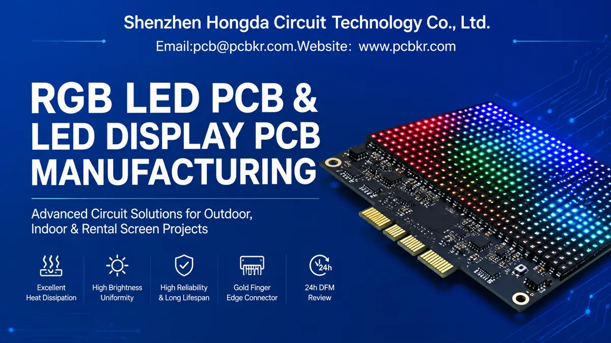
RGB LED PCB & LED Display PCB Manufacturing Solutions
RGB LED PCB and LED Display PCB Solutions for High-Brightness Digital Signage, Video Walls & Stage Screens
A failed LED display rarely dies because of the LEDs themselves. In most field returns our engineers review, the root cause traces back to the circuit board: thermal stress cracked a via, power rail imbalance created visible dimming zones, or signal integrity issues caused flicker at high refresh rates. The PCB is the silent foundation of every screen, yet procurement teams often evaluate it late in the sourcing cycle—after the LED brand and driver IC are locked in.
That approach costs money. Switching PCB suppliers mid-project because the first batch warped, delivered inconsistent color channels, or couldn’t survive outdoor thermal cycling burns 4–6 weeks and often forces a mechanical redesign. This article explains what defines a reliable LED display PCB, how material and process choices map to specific screen applications, and why Shenzhen Hongda Circuit Technology Co., Ltd. (PCBKR) manufactures these boards with the same equipment set we use for 224G AI server backplanes—precision that directly benefits your display project.
What Is an LED Display PCB and Why Does Your Screen Project Depend on It?
An LED display PCB is not a generic circuit board with LEDs soldered to it. It is a purpose-built electromechanical platform that distributes power to hundreds or thousands of LED nodes, carries high-speed serial data between driver ICs, and removes heat fast enough to keep junction temperatures below the threshold where lumen degradation accelerates. In a typical P3 indoor module, a single board might host 10,000+ SMD LEDs, 48 driver ICs, and power traces carrying 8–15A— all within a 320mm × 160mm footprint.
The Anatomy of a High-Performance RGB LED PCB Module
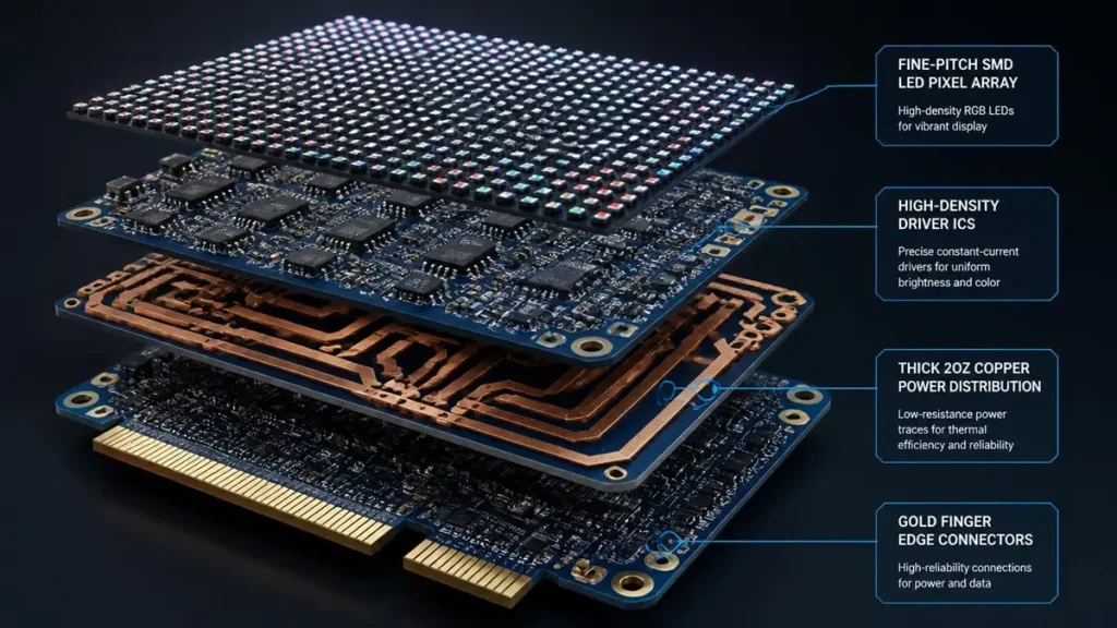
Exploded 3D view of a high-performance RGB LED PCB module, highlighting the SMD LED pixel array, driver IC zone, 2oz copper power distribution layer, and gold finger connectors.
A production-grade RGB LED PCB contains several functional zones that each introduce their own failure modes if underspecified:
The Pixel Array Area. This is where the RGB LEDs mount. Pad pitch, solder mask registration, and pad flatness determine how consistently each LED sits at the correct height. Even a 25μm height variation across a module creates visible “stair-step” brightness bands when tiles are butted together in a video wall.
The Driver IC Zone. Driver ICs like the MBI5124, ICN2038S, or TLC5947 require clean power and tightly controlled impedance on the clock and data lines. A poorly routed driver zone causes ghosting, color shift at low grayscale, or complete row failure when the board flexes during installation.
The Power Entry Section. High-brightness outdoor modules pull serious current. A 2oz copper minimum is standard for outdoor LED display PCB designs; 3oz or 4oz is common for stadium perimeter boards running at 10,000 nits. Thin copper here creates voltage drop, which translates directly to brightness non-uniformity across the module.
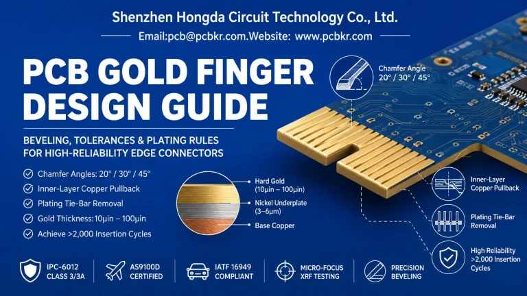
The Edge Connector / Gold Finger Interface. Rental and serviceable fixed-install screens rely on card-edge gold finger connectors for quick module swap-outs. These fingers must survive 500+ insertion cycles without plating wear exceeding 30μin of hard gold. Bevel angle, nickel underlayer thickness, and soldermask pullback all determine whether the module slides in smoothly or jams after six months of outdoor thermal expansion.
How PCB Quality Directly Impacts LED Screen Lifespan and Brightness Uniformity
Screen manufacturers specify 50,000-hour or 100,000-hour LED lifespans, but those numbers assume the PCB keeps the LEDs within their thermal envelope. When a board’s thermal resistance is too high—usually because of poor dielectric material in an aluminum core stack-up or insufficient thermal vias under the LED pads—the junction temperature climbs. Every 10°C increase above 85°C roughly doubles the lumen depreciation rate. Within 18 months, a screen that looked uniform at commissioning shows “yellowing” in the center of modules where heat pooled.
Signal integrity matters just as much. A RGB LED PCB carrying PWM data at 20MHz+ to 10,000 pixels is essentially a high-speed digital board. Reflections from unterminated stubs, crosstalk between adjacent data lines, or ground bounce from poorly designed power delivery networks all show up as visual artifacts: jittering pixels, color banding, or flash-on-camera effects that ruin a live broadcast.
RGB LED PCB vs. Standard LED PCB: Technical Differences That Determine Display Quality
Buyers sometimes assume a “LED PCB” is a single commodity category. That mistake leads to specifying a standard single-layer FR4 board for a full-color outdoor application, then wondering why the screen failed within two monsoon seasons. The gap between a basic LED PCB and a true RGB LED PCB engineered for display applications is wide enough to destroy project margins.
PWM Color Control and Signal Integrity in Full-Color LED Displays
A standard single-color LED PCB only needs to switch power on and off. A RGB LED PCB must deliver three independent PWM channels per pixel, synchronized across the entire module, with timing precision tight enough to maintain 14-bit or 16-bit grayscale. At 16-bit grayscale and 3840Hz refresh rate, the PWM period is roughly 4.3μs. If the PCB trace introduces 200ps of skew between the red and green clock lines, that timing error accumulates across 10,000 pixels and produces visible color drift.
This is why Hongda’s display PCB designs use stripline or microstrip routing for clock and latch signals, with matched-length tolerances held to ±50μm. Our LDI imaging system (SCREEN Ledia) images these fine traces directly onto photoresist without film distortion, which matters when you’re controlling impedance on 0.1mm-wide differential pairs.
Why Refresh Rate and Grayscale Performance Start at the PCB Level
You cannot fix a bad PCB with software. If the power rails sag under peak current draw because the copper weight was underspecified, the driver ICs brown out momentarily and drop grayscale bits. The result: a screen that is supposed to display smooth gradients instead shows posterized bands. Refresh rate claims above 1920Hz are meaningless if the PCB power distribution network (PDN) has too much DC resistance.
For high-refresh-rate LED display PCB designs, we specify:
- 2oz minimum copper on all power layers for modules above 5,000 nits
- Star-routed power entry to avoid daisy-chain voltage drop
- Local decoupling capacitors placed within 2mm of each driver IC’s power pins
- Ground plane integrity beneath every signal layer to control EMI
Material Selection Guide: Aluminum Core PCB vs. FR4 for LED Display Applications
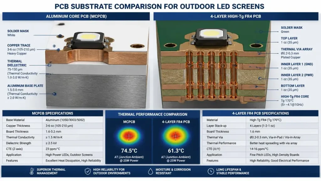
Cross-sectional comparison between an Aluminum Core PCB (MCPCB) for outdoor high-brightness displays and a 4-layer High-Tg FR4 stack-up with thermal via arrays, showing stack-up layers and thermal performance parameters.
Material selection is where most display PCB procurement decisions go wrong. The buyer either over-specifies and pays for aluminum core in an indoor retail application where FR4 would perform identically, or under-specifies and ships FR4 modules to a Middle Eastern outdoor site where ambient hits 55°C and the boards delaminate.
When to Specify Aluminum Core PCB for Outdoor High-Brightness Screens (≥10,000 nits)
Outdoor LED display PCB modules running at high brightness generate 30–60W per 320×160mm tile. FR4, with a thermal conductivity of roughly 0.3 W/m·K, cannot move that heat to the module’s rear heat sink fast enough. Aluminum core PCB (MCPCB) uses a thermally conductive dielectric layer (1.0–3.0 W/m·K) bonded to an aluminum base, dropping the thermal resistance path by an order of magnitude.
At Hongda, our aluminum LED display PCB stack-ups use 5052-H32 or 6061-T6 aluminum cores ranging from 1.0mm to 3.2mm thick, with dielectric breakdown voltage above 3kV to prevent creepage in wet environments. For high-power COB outdoor modules, we also offer thermoelectric separation designs where the LED thermal pad contacts the aluminum core directly, bypassing the dielectric entirely. This pushes effective thermal conductivity above 200 W/m·K in the critical heat path.
Specify aluminum core when:
- Module brightness exceeds 5,000 nits
- Ambient operating temperature spans -30°C to +60°C
- The installation faces direct solar load (digital billboards, stadium fascia)
- The design lifetime exceeds 5 years with <15% lumen depreciation
Cost-Optimized FR4 Solutions for Indoor Digital Signage and Retail Video Walls
Indoor digital signage running at 800–1,500 nits does not need aluminum. A well-designed multilayer FR4 LED PCB board with thermal via arrays under each LED pad and 2oz copper delivers adequate thermal performance at roughly 60–70% of the aluminum core cost. FR4 also offers better dimensional stability for fine-pitch SMD mounting (P1.25 and below), where aluminum’s CTE mismatch with copper can cause pad registration drift over large panels.
For indoor LED video wall PCB projects, we typically recommend high-Tg FR-4 (Tg 170°C) with filled thermal vias (0.2mm diameter, 0.5mm pitch under LED arrays) and a 4-layer stack-up: signal / ground / power / signal. This provides clean impedance control for the driver data lines while keeping the power plane close enough to the surface to minimize loop inductance.
Thermal Via Arrays and 2oz+ Copper: Preventing Hot Spots in Dense LED Arrays
Even with the right substrate, local hot spots kill modules. In a P2.5 RGB LED PCB, LEDs are packed at 400 per square inch. Without thermal vias conducting heat from the top copper layer down to the internal power plane or aluminum core, the center LEDs run 15–25°C hotter than edge LEDs. That delta produces a “bullseye” dimming pattern visible on white content.
Our design rule for thermal management LED display circuit boards: place a 0.3mm plated via directly under each LED’s thermal pad, with a 1.0mm array pitch, and tie it to the nearest internal copper plane. For outdoor modules, we fill these vias with thermally conductive epoxy to prevent solder wicking during assembly while maintaining the heat path.
Industry-Specific LED Display PCB Solutions by Application
Procurement teams rarely need a “generic” display PCB. They need a board that solves the specific mechanical, thermal, and electrical constraints of their end market. The following breakdown maps common buyer pain points to the PCB specifications that actually solve them.
Outdoor Advertising & Digital Billboard PCB: Weatherproof, High-Luminance Design
Pain point: A billboard PCB must survive thermal shock (day/night cycling), humidity, salt air in coastal regions, and direct UV exposure—while delivering 8,000+ nits for daylight readability.
Hongda’s outdoor LED display PCB specification:
- Base material: 2.0mm aluminum core PCB with high-Tg dielectric
- Copper weight: 3oz top layer, 2oz internal power plane
- Surface finish: ENIG + selective hard gold on edge connectors (30μin minimum)
- Soldermask: White or black LS-ink for UV resistance and reflectivity optimization
- Protection: Conformal coating (acrylic or silicone) over driver ICs and connectors
- Gold finger bevel: 45° chamfer, 0.5mm minimum distance from board edge to prevent copper burr
Stage Rental & Event Display PCB: Lightweight Modules with Quick-Maintenance Gold Finger Connectors
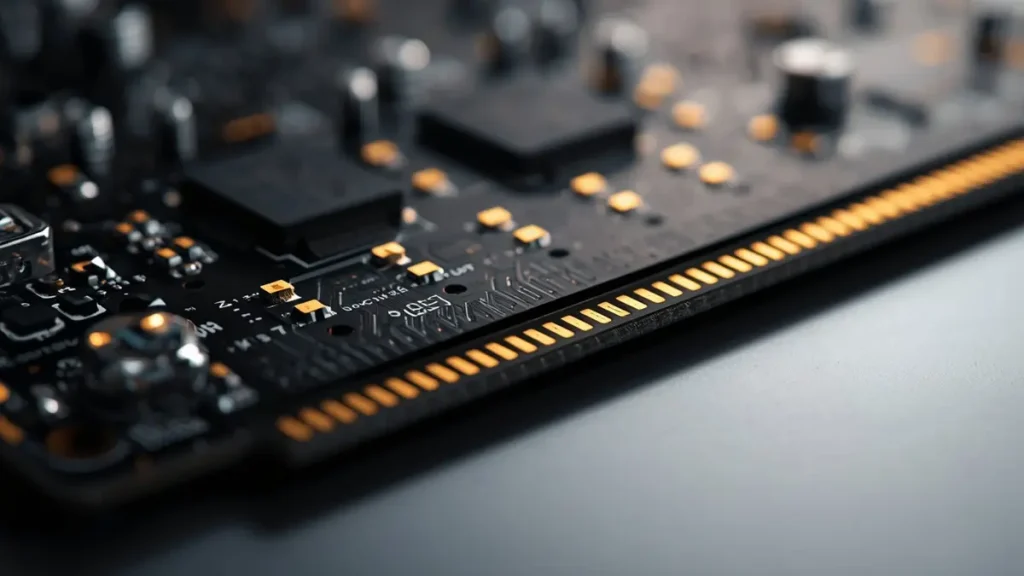
Close-up view of electroplated hard gold finger connectors with a precision 45° bevel on an LED display PCB, designed for high-cycle insertion durability in stage rental screens.
Pain point: Rental modules are handled roughly, assembled and disassembled weekly, and must be field-serviceable in under 90 seconds. Connector wear and mechanical damage are the top failure modes.
Our LED screen PCB module designs for rental applications integrate gold finger edge connectors with segmented finger layouts (long/short fingers) to ensure polarity protection during insertion. The 45° bevel angle allows one-handed module seating even when rack tolerances stack up. We use 1.6mm FR4 or lightweight aluminum (1.0mm core) to keep module weight under 8kg per 500×500mm cabinet. Driver ICs are placed on the non-LED side with magnetic-mount compatibility for front-service designs.
Command Center & Control Room PCB: 7×24 Reliability with COB and Fine-Pitch SMD
Pain point: Control rooms run continuously. A single dead pixel in a 4K video wall is visible from 10 feet away, and module replacement requires shutting down the entire wall section.
For command center LED display PCB production, we emphasize:
- COB (Chip-on-Board) compatibility: Direct LED die attach to the PCB with wire bonding. This eliminates SMD package failure modes and improves thermal path.
- Impedance-controlled routing: 100Ω differential pairs for clock/data with ±5% tolerance, verified with TDR testing on first articles.
- Redundant power rails: Dual-entry power design so a single open trace doesn’t kill half the module.
- Burn-in protocol: 72-hour full-white burn-in at 45°C ambient before shipment. Dead pixels and early driver IC failures are caught in Shenzhen, not in the client’s NOC.
Transportation & Public Information PCB: Wide-Temperature, Anti-Vibration, EMC-Compliant
Pain point: Airport FIDS boards, highway variable message signs, and rail platform displays must operate from -40°C to +85°C, survive constant vibration, and pass EMC emissions testing without external shielding.
Our transportation LED display PCB designs use:
- High-Tg, halogen-free FR4 or aluminum core with glass transition above 170°C
- Anti-vibration reinforcement: Heavier copper (3oz+) and stitched vias along the board perimeter to prevent corner cracks
- EMC control: Solid ground planes, controlled rise-time routing, and ferrite bead integration on data entry points
- Conformal coating: Parylene C or urethane for moisture and salt fog protection
Gaming Peripheral & Consumer RGB PCB: Per-Key Addressable Lighting with USB-C Integration
Pain point: Gaming keyboards and RGB peripherals compete on lighting effects. Buyers need per-key addressable control, low latency sync with game events, and USB-C power delivery compatibility.
Hongda manufactures custom RGB LED PCB boards for peripheral OEMs using:
- 2–4 layer FR4 with integrated STM32 or similar MCU
- WS2812B or SK6812 addressable LED chains with 0.1mm trace/space routing (enabled by our mSAP process)
- USB-C PD compatibility with 5V/3A power rail design
- ESD protection on all external connectors (IEC 61000-4-2 Level 4)
2026 PCB Manufacturing Technologies Behind Reliable LED Display Boards
The LED display industry is not standing still. Pixel pitches are shrinking below P1.0, refresh rates are pushing 7680Hz for broadcast cameras, and module power densities keep climbing. Building boards that keep up requires manufacturing technology that was considered “AI-server grade” just three years ago. At Hongda, we run the same equipment line for LED display PCB fabrication that we use for 224G PAM4 backplanes—because the precision requirements now overlap.
Laser Direct Imaging (LDI) for Ultra-Fine LED Pad Pitch and Solder Mask Accuracy
Traditional film-based photolithography introduces alignment errors (±15μm typical) and dimensional instability when humidity shifts. For P1.25 and finer LED modules, that error consumes your entire solder mask clearance budget.
Our SCREEN Ledia LDI system images directly onto dry-film photoresist using a 405nm laser source, achieving ±5μm layer-to-layer registration. This matters when you’re routing between 0.15mm LED pads or placing 0.4mm-pitch QFN driver ICs. LDI also eliminates the film remaking delay when you revise a pad size or adjust soldermask pullback around gold fingers—prototypes ship faster because the “film” is just a Gerber file.
mSAP Semi-Additive Process for High-Density Driver IC Routing
Standard subtractive etching struggles below 50μm line/space. As LED modules integrate more driver channels per IC and add local MCUs for smart pixel correction, the routing density in the driver zone exceeds what normal etch can deliver cleanly.
Hongda’s mSAP (modified semi-additive process) line plates copper onto a thin seed layer, then flash-etches the excess. We routinely achieve 8μm/8μm line/space with uniform sidewall profiles. On a recent P1.56 rental module project, mSAP allowed us to route 96 driver channels plus power and ground in a 4-layer stack-up that would have required 6 layers with conventional processing—saving the customer 18% on laminate cost while improving signal integrity.
AI-Driven AOI and X-Ray Inspection: Eliminating Cold Joints Before They Reach Your Assembly Line
A single cold solder joint on a driver IC’s ground pad can cause intermittent row failure that only shows up after 200 thermal cycles. Catching it after assembly at your factory costs a full module scrap. Catching it at our factory costs a 30-second rework cycle.
Our production line uses AI-enhanced automated optical inspection (AOI) with deep-learning defect classification, backed by Nordson DAGE X-ray inspection for BGA and QFN void analysis. The AI system was trained on millions of LED module solder joints and flags anomalies like insufficient heel fillet, tombstoning, or void percentages above 25% in thermal pads. First-pass yield on display PCB assembly runs at our facility consistently exceeds 99.5%, which means you receive boards that pass your incoming inspection without argument.
Precision Gold Finger Plating and Beveling for Edge Connector Durability in Rental Modules
Gold fingers on rental LED modules see abuse. Rough insertion, misaligned racks, and grit from outdoor sites all attack the plating. A 10μin ENIG finger might survive 50 insertions; a rental module needs 500+.
Hongda’s in-house gold finger plating line deposits 30–50μin electroplated hard gold over 150–200μin nickel on edge connector pads. We then precision-bevel the insertion edge at 20°–45° (customer-specified) using CNC chamfering with secondary optical alignment. For long/short finger designs, we maintain ±0.05mm length tolerance to ensure the ground fingers mate before power, preventing hot-plug arcing. Every batch is verified with XRF thickness measurement and cross-sectional microscopy on first articles.
Why Procurement Teams Choose Shenzhen Hongda Circuit Technology for LED Display PCB Production
Selecting a LED display PCB supplier is not a spreadsheet exercise. The lowest unit price often masks hidden costs: incoming inspection rejections, field failures at 14 months, or engineering teams spending hours on conference calls explaining why the latest batch doesn’t match the golden sample. Here’s how Hongda eliminates those hidden costs.
From 2-Layer Prototypes to 104-Layer Backplanes: Scalable Manufacturing Without Switching Suppliers
Many display projects start as 2-layer prototypes, then scale to 8-layer production modules, and eventually require complex controller backplanes. Switching suppliers at each phase introduces re-qualification risk and NRE duplication.
Hongda’s capability spectrum covers the entire journey. We build 2-layer quick-turn RGB LED PCB prototypes in 48 hours for proof-of-concept, then scale to volume production of 8-layer aluminum core modules with the same process controls, and finally manufacture the 40+ layer system backplanes that drive the entire wall. Your procurement team maintains a single vendor record, a single quality agreement, and a single point of accountability.
In-House mSAP, LDI, and Laser Drilling: Equipment That Matches AI-Server Precision Standards
Our 2026 equipment lineup includes:
- SCREEN Ledia LDI for ±5μm imaging precision
- Mitsubishi CO₂/UV hybrid laser drilling for 50μm microvias and blind/buried via structures
- mSAP plating line for 8μm/8μm fine-line capability
- Nordson DAGE X-ray and 3D AOI for defect detection above 99.9%
This is not equipment you find in a generic PCB job shop. It is the same precision infrastructure required for 224G PAM4 signal integrity—repurposed for the exacting demands of fine-pitch LED modules. When your P1.25 module requires 0.1mm trace/space and 0.2mm laser-drilled microvias under every LED pad, we do not subcontract. We build it in-house in our Shenzhen facility.
IPC Class 3, AS9100D, and IATF 16949: Quality Systems That Reduce Your Incoming Inspection Burden
Incoming inspection is a non-value-add cost. Every hour your IQC team spends arguing with a supplier about pad dimensions or solder mask registration is an hour not spent on your core product.
Hongda operates under IPC-6012 Class 3/3A, AS9100D (aerospace), and IATF 16949 (automotive) quality systems. What this means practically: our process capability indices (Cpk) for critical dimensions are maintained above 1.67, and we ship first-article inspection reports (FAIR) with every new part number, including cross-sectional photos, impedance test coupons, and thermal cycle data. Most LED display OEMs who transition to Hongda reduce their incoming inspection sampling rate by 50–70% because the data package we provide replaces their need for destructive verification.
24-Hour DFM Review and 48-Hour Prototype Turnaround: Accelerating Your Time-to-Market
In the display industry, trade show deadlines do not move. Missing a CES or ISE launch window by two weeks because your PCB supplier is “reviewing the files” destroys the business case.
Our engineering team returns DFM reviews within 24 hours of Gerber submission. We flag issues like insufficient soldermask clearance around gold fingers, trace necking under LED thermal vias, or power rail voltage drop before you commit to tooling. Standard prototypes ship in 48 hours; complex multilayer aluminum core LED display PCB prototypes in 5 days. When your competitor is still waiting for their second spin, your module is already in optical calibration.
LED Display PCB Procurement FAQ: What Buyers Ask Before Placing Volume Orders
How Do I Verify That a RGB LED PCB Manufacturer in China Can Actually Build to My Specs?
Do not trust the website. Request three things on your first call: (1) a live video walkthrough of their imaging and plating lines, (2) cross-sectional photos of a board with similar layer count and copper weight to your design, and (3) a first-article report from a current customer in the LED display industry (with the customer’s name redacted for confidentiality). At Hongda, we provide all three within 24 hours of an RFQ. If a supplier hesitates, they are likely brokering the job to a third party.
What Is the Real Difference Between Aluminum Core PCB and FR4 for Outdoor LED Screens?
The difference is thermal resistance, not just “heat dissipation.” Aluminum core PCB drops the junction-to-ambient thermal path by roughly 60–80% compared to standard FR4. In practical terms: an outdoor module running at 8,000 nits on FR4 will hit 105°C junction temperature in 35°C ambient. On aluminum core, the same module runs at 78°C. That 27°C delta translates to approximately 3× longer LED life. For indoor screens below 2,000 nits, FR4 with thermal vias is adequate and saves 25–35% on material cost.
Why Do My LED Modules Show Color Inconsistency After Six Months, and Can the PCB Fix It?
Color shift over time is usually a thermal problem masquerading as an LED problem. When the PCB cannot spread heat evenly, center LEDs age faster than edge LEDs. The center LEDs then emit a slightly different wavelength and lower lumen output. A properly designed LED display PCB with thermal via arrays, adequate copper weight, and correct aluminum core dielectric selection prevents this gradient. We also recommend specifying driver ICs with built-in dot-correction (like MBI5153) and designing the PCB to support calibration data storage on each module.
What Gold Finger Specifications Do I Need for Rental LED Modules That Are Swapped Weekly?
Rental modules need hard gold, not ENIG. Specify 30μin minimum electroplated hard gold over 150μin nickel on the edge connector pads. The insertion edge requires a 30°–45° bevel, and the soldermask must be pulled back at least 10 mils from the gold finger edge to prevent chipping during insertion. For long/short finger designs, maintain 0.1mm length tolerance to ensure sequential mating. Hongda’s in-house plating line verifies every batch with XRF; we reject fingers that measure 29μin even if the customer spec says 30μin minimum.
How Do I Reduce Lead Time Risk When Procuring Custom LED Display PCBs in Volume?
Lead time risk in 2026 comes from two sources: raw material allocation (especially high-Tg FR4 and aluminum core dielectrics) and capacity constraints at factories with advanced imaging capability. Mitigate both by locking in a blanket order framework with your supplier. At Hongda, we offer Kanban-style inventory programs for display PCB customers: we hold 4–6 weeks of finished-goods buffer stock in Shenzhen based on your forecast, and you pull against it with 7-day call-offs. This eliminates your exposure to 12-week laminate lead times while keeping your inventory carrying cost near zero.
Ready to source your next RGB LED PCB or LED display PCB project?
Upload your Gerber files, stack-up requirements, and application notes to sales@pcbkr.com. Our engineering team will return a complimentary DFM review, material recommendation, and detailed quotation within 24 hours. For urgent prototypes, mention your target date in the subject line—we have shipped display PCB first articles in 48 hours for customers who needed to hit a trade show deadline.
Shenzhen Hongda Circuit Technology Co., Ltd. Website: www.pcbkr.com | Email: sales@pcbkr.com | Phone: +86 0755 23720053 Certifications: ISO 9001:2015 | AS9100D | IPC-6012 Class 3/3A | ISO 13485 | IATF 16949
This article was prepared by the engineering team at Shenzhen Hongda Circuit Technology Co., Ltd. and reflects actual manufacturing capabilities, equipment specifications, and quality protocols in use at our Shenzhen facility as of August 2026. All technical claims are verifiable upon request.
About Author
David Chen https://www.linkedin.com/in/pcbcoming
David Chen boasts an extensive professional background in PCBA manufacturing, PCBA testing, and PCBA optimization, with specialized expertise in high-precision PCBA fault analysis and rigorous PCBA reliability testing. The author has worked with high-layer-count server PCB fabrication, ultra-low-loss backplane stackups, and thermo-mechanical reliability optimization for AI infrastructure projects involving 112G and 224G PAM4 architectures. Skilled in complex circuit design and cutting-edge advanced PCB manufacturing processes, he delivers solutions that elevate product durability and performance across industrial applications. His technical articles focusing on PCBA manufacturing workflows and testing methodologies are widely cited by industry peers, research institutions, and technical platforms, solidifying his reputation as a recognized technical authority in the global circuit board manufacturing sector.