LED PCB Assembly Services | High-Precision SMD LED Assembly & LED PCBA Manufacturing
When a procurement manager searches for LED PCB assembly services, the decision is rarely about price alone. It is about whether the finished LED PCBA will light up consistently in the field, survive thermal cycling, and arrive on time without hidden solder defects. At Shenzhen Hongda Circuit Technology Co., Ltd., we manufacture SMD LED assembly solutions for commercial lighting, automotive interior modules, and industrial indicator systems. Our facility in Shenzhen runs six fully automated SMT lines, integrated 3D SPI, AOI, and X-Ray inspection, plus nitrogen reflow ovens calibrated specifically for heat-sensitive LED components.
This page explains how we control every variable that determines whether your custom LED PCB assembly project succeeds or fails in mass production.
What Is LED PCB Assembly? Understanding SMD LED Assembly for Reliable LED PCBA Production
LED PCB assembly is the process of mounting surface-mount device (SMD) LEDs, driver ICs, resistors, and capacitors onto a printed circuit board, then soldering them into a functional LED PCBA. Unlike general-purpose PCB assembly, SMD LED assembly demands extreme placement accuracy, thermal management discipline, and polarity verification because LEDs are unidirectional, heat-sensitive, and often arranged in dense matrices where a single misaligned diode creates visible banding.
LED PCB Assembly vs. Standard PCBA: Why LED Applications Demand Specialized SMT Processes
Standard PCB assembly lines treat LEDs like any other passive component. That is a mistake. LEDs have a narrow process window: excessive reflow temperature degrades phosphor coating and reduces lumen maintenance; incorrect polarity causes immediate functional failure; and thermal vias must align precisely with the LED thermal pad to prevent junction temperature creep. At Hongda Circuit, our high-precision SMT LED assembly lines use closed-loop pressure feedback pick-and-place heads and bottom-camera fly alignment to compensate for component-center offset during pickup. This matters because a 50μm shift on a 3535 SMD LED creates a visible hot spot in a linear lighting module.
High-Precision SMT Assembly for SMD LEDs: Placement Accuracy That Eliminates Rework
Procurement teams evaluating an LED PCB assembly manufacturer in China often ask one question first: What is your placement accuracy? The answer determines whether you receive boards that pass AOI or boards that pass real-world thermal and optical testing. Our SMT lines are configured for LED-specific production, not retrofitted general-purpose assembly.
Accurate SMD LED Placement with ±25μm Repeatability
We run Yamaha YRM high-speed modular mounters with a placement accuracy of ±25μm at 3σ. For SMD LED assembly for high-density LED arrays, this repeatability ensures that 0603, 0805, 2835, 3528, 5050, and even 01005 mini-LED packages land within pad boundaries across 1,000-unit production runs. The machines use component-recognition algorithms that distinguish LED polarity marks from solder-paste reflections, a common source of false-positive placement in generic SMT shops.
LED Polarity and Orientation Control for Zero Defects
A reversed LED does not simply fail to light; it blocks current in a series string, killing an entire segment. Our process control includes:
- Pre-placement polarity verification via feeder-slot barcode matching against the BOM
- Post-placement AOI with customized LED polarity detection libraries
- First-article inspection (FAI) before reflow, documented with photographs per IPC-A-610 Class 2/3 criteria
SMT Assembly Consistency Across High-Density LED Arrays
In aluminum LED PCB assembly for COB and Mini-LED backlight applications, consistency across the panel determines uniformity. We control stencil aperture area ratios (typically 0.66 for 100μm-thick laser-cut stencils) to ensure equal solder-paste volume under every LED thermal pad. Uneven paste deposition creates tilted LEDs, which project light at divergent angles. Our 3D SPI system measures volume, height, and offset before the board enters the reflow oven, catching 70% of potential defects at the print stage.
Controlled Reflow Soldering for LED PCBA: Temperature Profiles That Protect Your Components
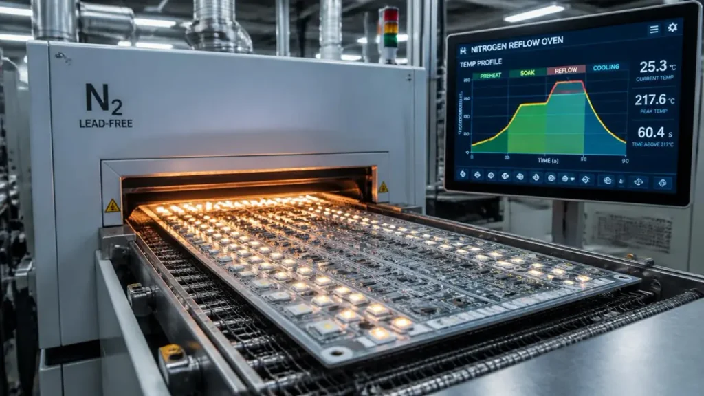
LED PCB Assembly Controlled Nitrogen Reflow Soldering Process
The reflow stage is where most LED PCBA failures originate. LEDs are not tolerant of the aggressive profiles used for standard IC assemblies. At Hongda Circuit, every LED PCB assembly with controlled reflow profile is treated as a custom thermal job.
Reflow Temperature Profile Control for Heat-Sensitive LEDs
We segment our 10-zone nitrogen reflow ovens into four critical phases:
- Preheat (150–180°C): 90–120 seconds to activate flux without shocking the LED epoxy lens
- Soak (180–210°C): 60–90 seconds to equalize delta-T across aluminum substrates
- Reflow (Peak 235–245°C): TAL (time above liquidus) held to 60–75 seconds for SAC305 lead-free solder, minimizing IMC growth while ensuring wetting
- Cooling (2–4°C/s): Controlled ramp to prevent thermal shock and solder joint fracturing
This profile is validated with a KIC thermal profiler and a 6-channel thermocouple fixture before the first production board enters the oven.
Solder Joint Reliability Through Nitrogen-Enhanced Reflow
Oxygen levels inside our reflow zones are maintained below 500ppm using nitrogen inerting. For turnkey LED PCB assembly services, this reduces oxidation on LED pads and improves wetting on thermally challenging aluminum-core PCBs. The result is fewer voids under thermal pads, lower contact resistance, and measurably better heat dissipation from LED junction to substrate.
Reflow Process Verification with Real-Time Thermal Monitoring
We do not rely on oven setpoints. Every production lot is verified against the golden thermal profile stored in our MES system. If zone temperatures drift by more than ±3°C, the line halts automatically. This is how we prevent the “soft failure” profile—where LEDs solder adequately but suffer accelerated lumen depreciation due to invisible thermal damage.
X-Ray Inspection for LED PCB Assembly: Seeing What AOI Cannot
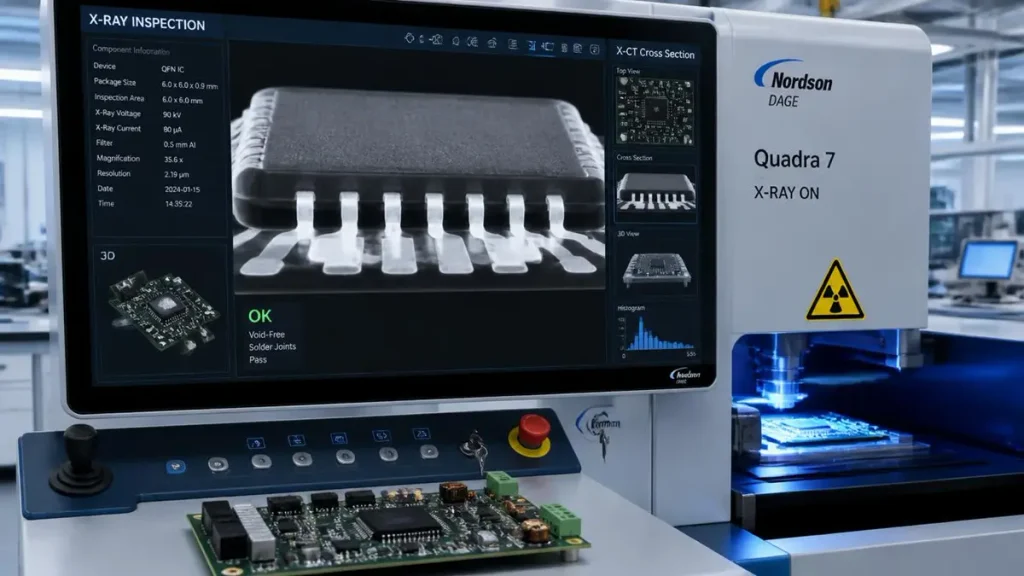
3D X-Ray Inspection for LED PCB Assembly Solder Joints
AOI cameras inspect what they can see. But modern LED drivers use QFN packages, and high-power LED modules use bottom-terminated thermal pads. These joints are invisible from the top. That is why LED PCB assembly with X-Ray inspection is not optional for reliability-critical projects—it is a risk-mitigation requirement.
Inspection of Hidden Solder Joints in BGA and QFN LED Drivers
Our 3D X-Ray inspection system (Nordson DAGE) generates cross-sectional slices through solder joints beneath QFN-32 LED driver ICs and DFN packages. We measure void percentage, ball roundness, and heel fillet coverage. A void rate above 25% under a thermal pad triggers automatic rework, because trapped air insulates the LED driver, causing thermal runaway in continuous operation.
Solder Quality Verification for Long-Term LED PCBA Reliability
X-Ray data is correlated with the board’s unique serial number in our traceability database. If a field failure occurs six months after shipment, we can recall the exact X-Ray image, reflow profile, and component lot for root-cause analysis. This level of documentation is what separates a reliable LED PCB assembly supplier in Shenzhen from a trading company that outsources to anonymous subcontractors.
Project-Based X-Ray Inspection Tailored to Your LED Assembly Requirements
Not every LED board needs full X-Ray coverage. For a simple 0805 indicator LED on FR-4, AOI suffices. For a 12W aluminum MCPCB with a DFN-8 buck converter and 36-series SMD LEDs, we recommend 100% X-Ray on the driver section plus AQL sampling on the LED array. Our engineering team defines the inspection scope during DFM review, so you do not pay for unnecessary testing, nor do you miss critical coverage.
LED PCBA Aging Test: Validating Performance Before Shipment
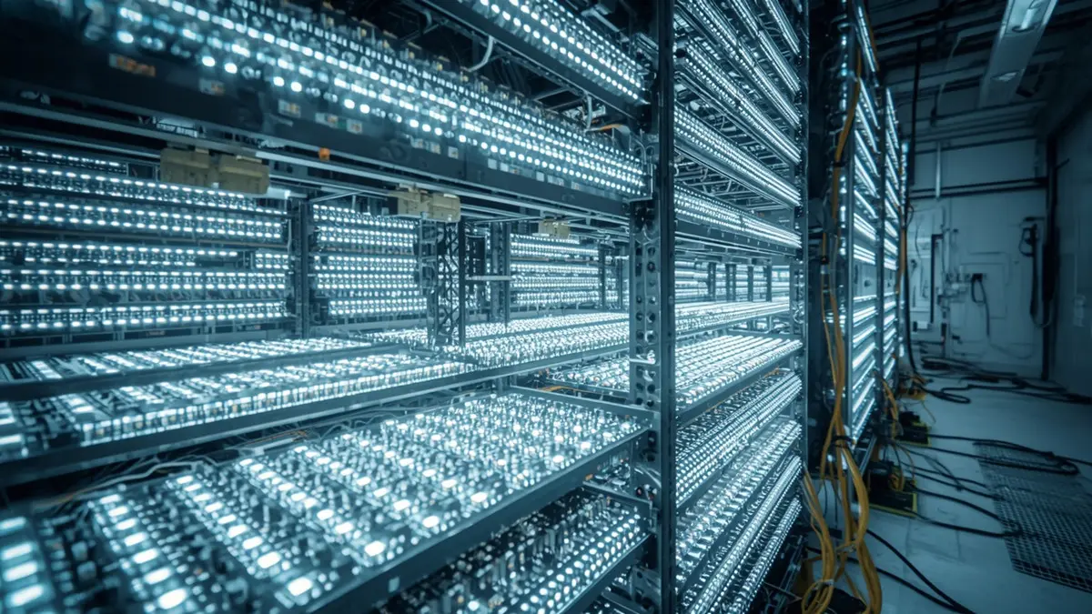
LED PCBA Burn-In and Aging Test Facility
A board that passes electrical test at 25°C may still fail after 500 hours in a 60°C ceiling fixture. That is why LED PCBA aging test and protective packaging are inseparable in our quality system.
LED PCBA Aging Test Protocols for Commercial and Industrial Lighting
We operate dedicated aging racks with programmable DC sources and data loggers. Standard protocols include:
- 48-hour continuous burn-in at rated current and 45°C ambient
- Thermal cycling between -20°C and +85°C for 10 cycles (on request)
- Lumen maintenance spot-checks using an integrating sphere (available for pilot runs)
During aging, we monitor for flicker, color shift, and catastrophic failure. Boards that exhibit lumen depreciation >5% are quarantined for failure analysis.
LED Lighting Performance Verification: Lumen Maintenance and Color Stability
For white-light SMD LED assembly projects, we verify that CCT (correlated color temperature) remains within the specified bin range after burn-in. A shift from 4000K to 4300K after 48 hours indicates a soldering thermal profile that damaged the phosphor layer—something no standard ICT can detect.
Test Result Control and Traceability for Batch Acceptance
Aging test results are compiled into a COA (Certificate of Analysis) per lot. Procurement managers use this document to validate batch acceptance without running their own incoming inspection. For low MOQ LED PCB assembly for lighting startups, this eliminates the capital expense of building an in-house burn-in lab.
Protective Packaging and Logistics for LED PCBA: Delivering Boards Intact
An assembly that survived SMT, reflow, and testing can still be destroyed by static discharge or moisture ingress during shipping. Our LED PCB assembly lead time and quality control commitment extends to the moment the package arrives at your dock.
Anti-Static and Moisture-Barrier Packaging for Sensitive LED Assemblies
Finished LED PCBA units are sealed in anti-static vacuum bags with desiccant and humidity indicator cards. For aluminum-core boards with exposed metal edges, we add ESD foam inserts to prevent pad scratching. Moisture-sensitive LED drivers (MSL 3 or higher) are baked at 125°C for 4 hours before sealing, complying with J-STD-033B handling requirements.
Packaging Identification and Batch Traceability
Every carton carries a barcode label linking to the production batch, reflow profile ID, and component lot numbers. If you receive a partial shipment, the label tells you exactly which SMT run those boards came from. This granularity is essential for LED PCB assembly component sourcing solutions where traceability audits are mandatory.
Shipping and Logistics Coordination from Shenzhen to Global Destinations
We coordinate DHL, FedEx, and air freight based on your Incoterms. For turnkey LED PCB assembly services involving multiple SKUs, we consolidate shipments and provide packing lists with harmonized tariff codes. Our logistics team pre-scans export documentation to reduce customs clearance delays in the EU, US, and Southeast Asia.
LED PCB Assembly Process: From BOM Review to Final Delivery
When you request an LED PCB assembly quote, this is exactly what happens inside our Shenzhen facility:
| Step | Process | Control Point |
|---|---|---|
| 1 | Production Information Review | BOM validation, component availability check, DFM feedback within 24 hours |
| 2 | SMD LED SMT Placement | 3D SPI paste inspection → Yamaha high-speed placement → post-placement AOI |
| 3 | Reflow Soldering | Nitrogen profile, KIC thermal verification, real-time MES monitoring |
| 4 | Assembly Inspection | AOI for polarity, offset, and solder defects |
| 5 | X-Ray Inspection | 3D X-Ray on QFN/BGA/thermal pads per project scope |
| 6 | Aging Test | 48-hour burn-in at rated current with lumen and thermal monitoring |
| 7 | Packaging and Shipment | ESD vacuum seal, batch labeling, and logistics coordination |
We do not insert steps we have not listed. If your project does not require X-Ray, we do not add it to inflate cost. If your LEDs are MSL 1 and your destination is dry, we do not force moisture-barrier packaging. This is how custom LED PCB assembly should work—scope-defined, not scope-inflated.
LED PCBA Quality Control: A Systematic Approach to Zero-Defect Manufacturing
| Quality Control Stage | What We Verify | Rejection Criteria |
|---|---|---|
| SMT Paste Print | Volume, height, offset via 3D SPI | >±50% volume deviation from nominal |
| SMD LED Placement | Position, polarity, rotation via AOI | >25% pad offset or reversed polarity |
| Reflow Soldering | Profile adherence via KIC profiler | Peak temp outside ±5°C of set profile |
| X-Ray Inspection | Void %, joint shape, heel fillet | Void >25% under thermal pads |
| Aging Test | Lumen maintenance, thermal stability | >5% lumen drop or CCT shift out of bin |
| Final Packaging | ESD integrity, label accuracy, moisture seal | Vacuum failure or incorrect batch label |
Our quality system is built around the reality that LED PCB assembly failures are expensive not because the board is costly, but because the failure happens inside your customer’s ceiling, vehicle, or surgical lamp. Prevention at the Shenzhen factory is cheaper than recall.
Request Your LED PCB Assembly Quote: Turnkey SMD LED Assembly from a Verified Shenzhen Manufacturer
If you are a procurement manager, hardware engineer, or lighting product manager evaluating how to choose an LED PCB assembly manufacturer, consider this: the lowest quote often hides the highest risk. A factory that cannot explain its reflow profile, cannot show X-Ray images, and cannot trace component lots is not a manufacturer—it is a broker.
At Shenzhen Hongda Circuit Technology Co., Ltd., we own the SMT lines, the nitrogen reflow ovens, the X-Ray machines, and the aging racks. We are not a trading company. When you visit www.pcbkr.com and submit an RFQ, you receive:
- A DFM report within 24 hours, flagging LED polarity risks and thermal via recommendations
- A transparent BOM analysis with alternate component suggestions for shortage mitigation
- A fixed lead-time commitment with milestone tracking, not a vague “4–6 weeks”
- Aging test and X-Ray data included in the delivery documentation
PCBA Instant Quote
Submit your Gerber, BOM, and quantity. We return a detailed quotation with process flow, test plan, and logistics options. Email: pcb@pcbkr.com
Component Sourcing Inquiry
If your BOM contains allocated LED drivers or hard-to-source SMD LEDs, our procurement team runs availability checks against authorized distributor stock before you commit to NRE.
LED PCB Assembly FAQ:
How Do I Verify a Real LED PCB Assembly Factory in Shenzhen vs. a Trading Company?
Ask for a live video walkthrough of the SMT floor, specifically the reflow oven brand, X-Ray machine model, and aging rack setup. A real factory will show you KIC profiler data and MES screenshots in real time. A broker will deflect or send stock photos. At Hongda Circuit, we schedule live factory tours via video call and provide ISO 9001 and IPC-A-610 certification documents with the quotation.
What Is the Typical Lead Time for SMD LED Assembly Prototypes vs. Production?
For SMD LED PCB assembly prototype runs (5–50 pieces) with in-stock components, our standard lead time is 5–7 working days including aging test. For production volumes (500–5,000 pieces), lead time scales to 10–15 working days depending on component procurement. If your LEDs or drivers are on allocation, we flag this during BOM review and propose pin-to-pin alternates from our authorized distributor network.
Why Does Reflow Temperature Control Matter More for LED PCBA Than Standard Boards?
LEDs contain phosphor coatings and epoxy lenses that degrade above 260°C. Standard ICs tolerate 260°C peak profiles; LEDs do not. Our LED PCB assembly with controlled reflow profile maintains peak temperature between 235–245°C with tight TAL control. This preserves lumen maintenance and color bin consistency, which directly affects your end product’s optical performance and warranty liability.
Can You Source Hard-to-Find LED Drivers and SMD LEDs During Component Shortages?
Yes. Our component sourcing team maintains relationships with authorized distributors for major LED brands (Nichia, Cree, Osram, Samsung) and driver IC suppliers (TI, ON Semi, Infineon). For LED PCB assembly component sourcing solutions, we cross-reference your BOM against real-time stock and suggest form-fit-function alternates if your primary part is on 52-week allocation. This is how we prevent the 60–80% of delays that originate from component unavailability.
What Packaging Standards Ensure My LED PCBA Arrives Without ESD or Moisture Damage?
We package all LED PCBA shipments in anti-static vacuum bags with desiccant and humidity indicator cards. For sea freight or high-humidity destinations, we add moisture-barrier bags with desiccant packs rated for 6-month protection. Aluminum-core boards receive edge-protecting ESD foam to prevent metal-edge shorting. Every package is labeled with the production batch, allowing traceability from our Shenzhen facility to your receiving dock.
Shenzhen Hongda Circuit Technology Co., Ltd.
Website: www.pcbkr.com
Business Scope: High-precision LED PCB assembly, SMD LED assembly, LED PCBA manufacturing, turnkey component sourcing, and global logistics from Shenzhen, China.
About Author
David Chen https://www.linkedin.com/in/pcbcoming
David Chen boasts an extensive professional background in PCBA manufacturing, PCBA testing, and PCBA optimization, with specialized expertise in high-precision PCBA fault analysis and rigorous PCBA reliability testing. The author has worked with high-layer-count server PCB fabrication, ultra-low-loss backplane stackups, and thermo-mechanical reliability optimization for AI infrastructure projects involving 112G and 224G PAM4 architectures. Skilled in complex circuit design and cutting-edge advanced PCB manufacturing processes, he delivers solutions that elevate product durability and performance across industrial applications. His technical articles focusing on PCBA manufacturing workflows and testing methodologies are widely cited by industry peers, research institutions, and technical platforms, solidifying his reputation as a recognized technical authority in the global circuit board manufacturing sector.