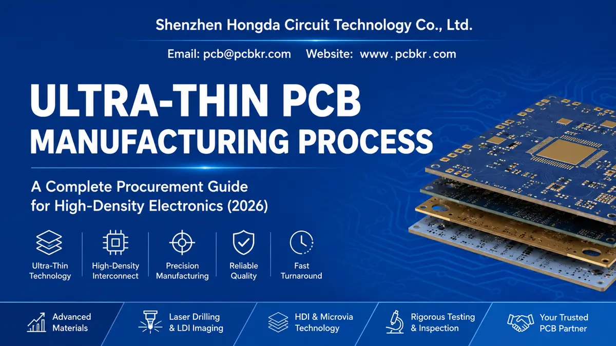
Ultra-Thin PCB Manufacturing Process: A Complete Procurement Guide for High-Density Electronics
Why Procurement Teams Struggle with Ultra-Thin PCB Sourcing
Ultra-Thin PCB Manufacturing Process demands extreme precision, rigorous process control, and advanced material handling capabilities that far exceed the requirements of standard commodity PCB production. Unlike conventional printed circuit boards, ultra-thin PCBs with a total thickness below 0.4 mm feature ultra-fine line/space resolution under 50 µm, microvias smaller than 100 µm, and strict impedance tolerance standards. Every production link, from substrate lamination and laser drilling to circuit imaging and surface finishing, requires tightly calibrated parameters and specialized equipment to avoid common defects such as board warpage, microvia failure, and impedance deviation. It is precisely the high technical threshold of professional ultra-thin PCB manufacturing processes that leads to widespread sourcing difficulties for procurement and hardware teams across the industry.
If you are a procurement manager or hardware engineer responsible for sourcing ultra-thin PCBs, you have likely encountered the same frustrating industry dilemma. Many ordinary PCB suppliers claim to support HDI production and promise precise dimensional tolerances and fast delivery cycles. However, the finished boards often suffer from irreversible quality issues during subsequent assembly and reliability testing. Typical problems include severe board warping that affects SMT assembly accuracy, microvia structural damage leading to circuit connection failure, and drifting impedance values that fail to meet design specifications. Critically, these recurring quality problems are rarely caused by isolated operational errors. Instead, they stem from incomplete and immature manufacturing workflows—an essential gap that distinguishes ordinary commodity PCB manufacturers from professional precision fabricators qualified to serve high-end scenarios.
Market demand further amplifies this sourcing challenge. The global PCB market is projected to reach $70.95 billion by 2026, among which the ultra-thin PCB and high-density interconnect (HDI) segments register the fastest growth. This robust growth is driven by the booming demand for 5G infrastructure construction, wearable medical devices, AI computing hardware, automotive electrification, and high-end consumer electronics. Despite the influx of manufacturers claiming HDI and ultra-thin PCB production capabilities, only a small number of suppliers can stably and reliably mass-produce qualified ultra-thin PCBs that meet stringent thickness, microvia, and line precision standards. The core competitiveness gap lies in professional production equipment, standardized full-process control systems, and sophisticated material application technology—all of which directly determine the field reliability and market launch efficiency of end products.
To solve the industry pain points of unstable ultra-thin PCB quality and uneven supplier capabilities, Shenzhen Hongda Circuit Technology Co., Ltd. has built a dedicated, fully optimized production line tailored to the core technical difficulties of ultra-thin PCB manufacturing. Our Shenzhen production base is equipped with Class 100 ultra-clean workshops, high-precision UV laser drilling systems, advanced Laser Direct Imaging (LDI) platforms, and professional semi-additive process (SAP) production lines, all of which are specially customized for ultra-thin substrate processing and high-precision circuit fabrication. This guide will elaborate on our standardized ultra-thin PCB manufacturing workflow step by step, providing clear and actionable technical evaluation criteria. You can use these professional standards to objectively assess and screen any ultra-thin PCB supplier, including us, to select the most reliable partner for your specific product applications.
Material Preparation — Selecting Ultra-Thin PCB Substrates for High-Density Applications
Substrate Selection Determines Everything That Follows
The first decision in ultra-thin PCB manufacturing is also the most consequential: choosing the right substrate material. Standard FR-4 laminates, typically 1.6 mm thick, are unsuitable for ultra-thin designs that require total board thickness below 0.4 mm or even 0.2 mm. For these applications, fabricators specify high-Tg, low-loss dielectrics, modified epoxy systems, or advanced materials like M9-grade copper-clad laminates (CCL) that support 224 Gbps signal transmission with dielectric loss (Df) as low as 0.0005 at 10 GHz.
Procurement Pain Point: Many buyers receive quotes based on generic material specifications, only to discover during first-article inspection that the substrate’s coefficient of thermal expansion (CTE) mismatches their component requirements, causing delamination after reflow.
What to Verify:
- Glass transition temperature (Tg): ≥ 170°C for standard applications, ≥ 200°C for high-reliability automotive or aerospace boards.
- Dielectric constant (Dk) and loss tangent (Df): Must be consistent across the frequency band your design operates in.
- Copper foil profile: HVLP (very low profile) or HVLP4/5 copper foil reduces signal loss at high frequencies and improves etch definition for fine lines.
- Thickness tolerance: Ultra-thin core materials require ±5 µm or better thickness control to prevent impedance variation across the panel.
At Shenzhen Hongda Circuit Technology, we maintain direct partnerships with leading laminate suppliers including Panasonic, Isola, and domestic M9-grade material producers. Every substrate lot undergoes incoming inspection for thickness, Dk/Df consistency, and copper peel strength before entering production. This upstream control eliminates the root cause of many downstream failures that less disciplined factories miss.
Panelization and Surface Preparation for Ultra-Thin Boards
Once material is selected, panels are cut to production size—typically 18 × 24 inches or customer-specified dimensions. For ultra-thin substrates, this step requires specialized depaneling equipment. Mechanical routing can induce microcracks in fragile cores, so laser depaneling or precision CNC routing with vacuum hold-down is standard for boards below 0.3 mm.
Surface preparation follows immediately. Panels undergo chemical cleaning to remove oxidation, organic contaminants, and handling oils. For ultra-thin copper foils (1/4 oz or 1/3 oz), this cleaning step is critical: any residual contamination will cause photoresist adhesion failure during imaging, leading to pinholes or line breaks after etching.
Key Specification to Request: Ask your supplier whether they use automated handling systems with carrier panels for ultra-thin substrates. Manual handling of 0.1 mm cores introduces wrinkles and creases that persist through lamination and ruin layer-to-layer alignment.
Inner-Layer Fabrication — Building Precision Circuitry for Ultra-Thin Multilayer PCBs
Photoresist Application and Circuit Pattern Formation
Inner-layer fabrication transforms raw copper-clad laminate into patterned circuit layers. The process begins with photoresist lamination. For ultra-thin PCBs requiring line/space below 50 µm, dry film photoresist thickness must be carefully matched to copper weight—typically 12 µm or 20 µm dry film for 1/3 oz copper. Thicker resist films prevent fine-line resolution; thinner films may not provide adequate plating sidewall protection.
Procurement Pain Point: Buyers often specify 3/3 mil (75 µm) line/space in their Gerber files without confirming whether the supplier’s imaging system can actually achieve this repeatably. Standard contact printing with film artwork struggles below 3/3 mil due to light scattering and film dimensional instability.
Shenzhen Hongda’s Approach: We use Laser Direct Imaging (LDI) for all inner-layer patterns on ultra-thin builds. LDI writes the circuit pattern directly onto photoresist using a UV laser, eliminating phototool film and its associated dimensional variation. Our LDI systems achieve ±8 µm registration accuracy and support line/space down to 25/25 µm on production volumes. For sub-25 µm features, we deploy modified semi-additive process (mSAP) lines that build traces through selective copper plating rather than subtractive etching.
Inner-Layer Etching and Automated Optical Inspection (AOI)
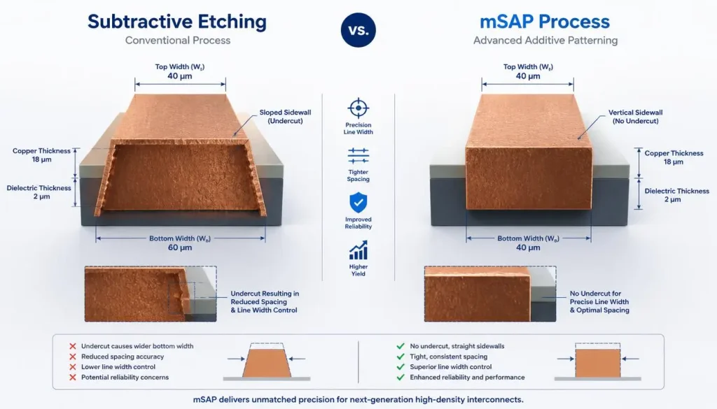
Detailed cross-section comparison between Subtractive Etching (left) with trapezoidal undercut and mSAP Process (right) with straight vertical sidewalls for ultra-thin PCB manufacturing.
After imaging, exposed copper is etched using cupric chloride or alkaline ammonia chemistry. For ultra-thin inner layers, etch uniformity is paramount. Over-etching reduces trace width below specification; under-etching leaves copper slivers that create short circuits after lamination.
Critical Control Parameter: Etch factor (the ratio of horizontal to vertical etch rate) must be optimized for thin copper. With 1/4 oz copper (≈ 9 µm), the etch window is narrow. Our process engineers monitor etch rate every 30 minutes using test coupons, adjusting conveyor speed and chemistry concentration to maintain trace width within ±10% of target.
Following etching, each inner layer undergoes 100% Automated Optical Inspection (AOI). Unlike sampling inspection, 100% AOI catches defects like open circuits, mouse bites, and residual copper before layers are laminated into a multilayer stack. Catching these defects at the inner-layer stage saves the entire board cost; rejecting a finished 12-layer board because of one inner-layer short is economically devastating.
Lamination — Achieving Layer-to-Layer Alignment in Ultra-Thin PCB Stackups
Stackup Design and Prepreg Selection for Ultra-Thin Multilayer PCBs
Lamination bonds inner layers, prepreg (B-stage resin), and copper foil into a solid multilayer structure. For ultra-thin PCBs, this step is where many fabricators fail. Standard multilayer boards tolerate some layer-to-layer misalignment, but ultra-thin HDI boards with microvias and fine-pitch BGA pads require ±25 µm or better layer registration—a tolerance that demands precision alignment systems and low-flow prepreg materials.
Procurement Pain Point: Buyers frequently receive boards where drilled microvias miss their target pads due to layer shift during lamination. This defect, called “pad annular ring violation,” is not always caught by electrical testing because the via may still connect electrically while creating a reliability hazard.
Stackup Considerations for Ultra-Thin Designs:
- Symmetrical construction: Asymmetric copper distribution causes board warp during lamination and reflow. We enforce symmetrical stackup rules unless the design specifically requires asymmetry with stiffener support.
- Low-flow prepreg: Standard prepreg resin flow can shift thin inner layers during lamination. Low-flow or no-flow prepreg materials minimize resin migration while providing adequate adhesion.
- Sequential lamination: For high-layer-count ultra-thin boards (20+ layers), sequential lamination builds the board in stages, reducing cumulative registration error. Each sub-assembly is drilled, plated, and inspected before the next lamination cycle.
Press Cycle Control and Thickness Uniformity
Our lamination presses operate with vacuum-assisted pressing and programmable multi-stage heat/pressure profiles. For ultra-thin boards, the pressure ramp rate is critical: too fast, and the thin core collapses or resin squeezes out excessively; too slow, and partial curing creates voids or delamination.
Post-lamination, every panel is measured for thickness uniformity using a scanning CMM (coordinate measuring machine). Thickness variation across a panel must be controlled to ±5 µm for ultra-thin designs to ensure subsequent drilling and imaging processes remain within tolerance.
Imaging — Laser Direct Imaging (LDI) Technology for Ultra-Fine PCB Features
Why LDI Replaces Traditional Film Imaging for Ultra-Thin PCBs
Imaging transfers the outer-layer circuit pattern onto copper foil. For ultra-thin PCBs with fine-pitch components, traditional film-based contact printing is inadequate. Film stretches with humidity changes, dust particles create pinholes, and mask-to-panel contact introduces edge definition loss.
Laser Direct Imaging (LDI) solves these problems by writing the pattern directly with a UV laser. The benefits for ultra-thin PCB manufacturing are substantial:
- No phototools: Eliminates film procurement lead time and storage costs.
- Dynamic scaling: LDI software compensates for material expansion/contraction in real time, critical for ultra-thin substrates that distort more than standard thickness boards.
- Fine-feature capability: LDI routinely achieves 20/20 µm line/space, with advanced systems reaching 15/15 µm.
At Shenzhen Hongda Circuit Technology, our LDI suite includes multiple systems for different production volumes. Prototype and small-batch orders run on high-resolution LDI platforms that can image 0.2 mm thick panels without vacuum table damage. High-volume orders use multi-head LDI systems that maintain throughput without sacrificing the ±8 µm registration accuracy required for microvia landing pads.
Photosensitive Material Selection for Ultra-Thin Substrates
Not all photoresists perform equally on ultra-thin copper. For mSAP processes, we use negative-tone dry film photoresists with high contrast ratios. These resists form vertical sidewalls during development, which is essential for creating rectangular trace profiles rather than the trapezoidal shapes produced by conventional subtractive etching.
Specification to Request: Ask whether your supplier uses LDI-compatible photoresist. Some factories run LDI hardware but continue using legacy photoresist formulations optimized for film exposure, negating much of LDI’s accuracy advantage.
Etching — Semi-Additive Process (SAP) for Ultra-Thin PCB Trace Definition
When Subtractive Etching Reaches Its Physical Limit
Standard subtractive etching removes unwanted copper by spraying etchant across the entire panel. This method works for line/space above 3/3 mil (75 µm), but below this threshold, undercutting becomes uncontrollable. A 25 µm wide trace in 18 µm thick copper will experience significant lateral etching, producing a trapezoidal cross-section with rounded top edges. For high-frequency signal integrity and fine-pitch BGA routing, this geometry is unacceptable.
Semi-Additive Process (SAP) and Modified Semi-Additive Process (mSAP) have become the industry standard for ultra-thin PCBs requiring sub-50 µm features. The workflow differs fundamentally from subtractive etching:
- Base copper deposition: A very thin seed layer of copper (2–5 µm) is electrolessly deposited across the entire panel.
- Photoresist patterning: Dry film photoresist is laminated, exposed (via LDI), and developed to create a mold where traces will form.
- Selective copper plating: Copper is electrolytically plated only in the open resist windows, building traces to the desired height (typically 15–20 µm).
- Resist stripping: The plating mold is removed.
- Seed layer etching: The thin seed copper between traces is flash-etched away, leaving only the plated traces.
Result: Near-rectangular trace profiles with vertical sidewalls, enabling tighter spacing without electrical shorting and improved impedance control for high-speed designs.
Etch Chemistry and Process Control for Ultra-Thin Boards
For boards that still use subtractive etching (line/space ≥ 50 µm), etch chemistry must be tightly controlled. We use cupric chloride regeneration systems that maintain etchant composition within ±2% of setpoints. For ultra-thin copper foils, etch time is reduced proportionally, and conveyor speed is increased to minimize undercut.
Quality Checkpoint: After etching, trace width is measured at five locations per panel using automated optical measurement systems. Any panel showing trace width outside ±10% tolerance is flagged for engineering review before proceeding to solder mask.
Drilling — Laser Microvia Drilling for High-Density Interconnect (HDI) Ultra-Thin PCBs
Mechanical Drilling vs. Laser Drilling for Ultra-Thin Substrates
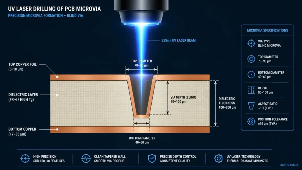
Engineering cross-section diagram of UV laser microvia drilling on an ultra-thin HDI substrate, showing layer structure, blind via geometry (<100 µm), and precise depth control.
Mechanical drilling with carbide drill bits is cost-effective for through-holes above 0.2 mm diameter. However, for ultra-thin PCBs with blind microvias connecting outer layers to adjacent inner layers, mechanical drilling is impractical. Drill bits below 0.15 mm diameter break frequently, and the aspect ratio (hole depth to diameter) limits reliable plating.
Laser drilling is the enabling technology for HDI ultra-thin PCBs. Two laser types dominate:
- CO₂ lasers: Best for drilling dielectric material after copper window opening. Typical via diameter: 75–150 µm. Drilling speed: 500–3,000 holes per second.
- UV lasers: Capable of drilling directly through copper foil without windowing. Typical via diameter: 25–100 µm. Superior hole quality with minimal heat-affected zone.
Procurement Pain Point: Buyers often discover too late that their supplier’s laser drill system cannot achieve the via diameter or positional accuracy their BGA pitch requires. A 0.4 mm pitch BGA requires microvias around 100 µm diameter with landing pads no larger than 250 µm. If the supplier’s laser has ±25 µm positional accuracy, via-to-pad alignment becomes marginal.
Shenzhen Hongda’s Capability: Our drill room houses UV laser systems with ±10 µm positional accuracy and CO₂ laser systems for high-speed production. We support microvia diameters down to 50 µm with aspect ratios up to 1:1 per IPC-6012 guidelines. For stacked microvia structures (essential for Any Layer HDI), we use sequential drilling and copper filling to ensure vertical alignment within ±15 µm across the entire stack.
Desmear and Via Wall Preparation
After laser drilling, resin smear from the ablation process coats the via walls and bottom pad. This smear must be completely removed before plating, or the via will exhibit high resistance or intermittent opens under thermal cycling.
Our process uses plasma desmear followed by chemical cleaning. Plasma etching with oxygen-rich gas mixtures removes resin smear uniformly, even in high-aspect-ratio vias where liquid chemistry struggles to penetrate. This step is non-negotiable for reliability: incomplete desmear is the #1 root cause of microvia field failures.
Plating — Copper Deposition and Via Filling in Ultra-Thin PCB Manufacturing
Electroless Copper and Electrolytic Plating for Microvia Reliability
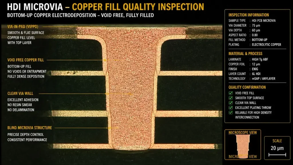
Metallurgical microsection view of a bottom-up electroplated copper-filled microvia in an ultra-thin HDI PCB, demonstrating void-free deposition and a flat top surface for VIPPO.
Plating establishes electrical conductivity through drilled holes and builds copper thickness on outer layers. For ultra-thin PCBs, plating must achieve two objectives simultaneously: adequate copper thickness (typically 20–25 µm in holes) and complete via filling for via-in-pad (VIPPO) designs.
The process begins with electroless copper deposition (≈ 0.5 µm) to make the hole walls conductive. This is followed by electrolytic copper plating, where panels are immersed in a copper sulfate bath with controlled current density. For microvias, current density is optimized to promote bottom-up filling rather than sidewall plating, which can create voids.
Via Fill Quality Metrics:
- Fill factor: ≥ 95% copper fill for reliable thermal and electrical performance.
- Dimple depth: ≤ 15 µm for VIPPO structures where solder joints form directly over the filled via.
- Via wall copper thickness: 20–25 µm to withstand thermal expansion stress.
At Shenzhen Hongda, our plating lines include pulse rectifiers that modulate current to enhance throwing power in high-aspect-ratio vias. After plating, every production lot undergoes microsectioning analysis—physical cross-sections of sample vias examined under microscope—to verify fill quality and copper thickness.
Surface Copper Thickness and Planarization
For ultra-thin PCBs with fine lines, outer-layer copper thickness after plating is typically 18–30 µm (0.5–1 oz equivalent). Thicker copper makes fine-line etching difficult; thinner copper may not carry sufficient current or withstand multiple thermal cycles.
For VIPPO boards, plated vias are planarized using chemical-mechanical polishing (CMP) to create a flat surface before solder mask application. Planarization tolerance is held to ±10 µm to ensure solder mask uniformity and prevent solder balling during assembly.
Solder Mask — Protecting Ultra-Thin PCB Circuitry with Precision Coating
Liquid Photoimageable (LPI) Solder Mask for Fine-Pitch Designs
Solder mask insulates copper traces, prevents solder bridging during assembly, and protects circuitry from environmental moisture. For ultra-thin PCBs with fine-pitch components, solder mask registration is critical: mask opening misalignment can cover BGA pads or leave excessive copper exposed.
We use Liquid Photoimageable (LPI) solder mask applied by curtain coating or screen printing, then exposed using LDI alignment systems. This direct imaging approach eliminates the registration errors associated with film-based solder mask exposure.
Key Specifications for Ultra-Thin PCBs:
- Mask thickness: 10–20 µm over traces, with dams between fine-pitch pads maintained at ≥ 50 µm width.
- Registration accuracy: ±20 µm to ensure pad openings align perfectly with copper features.
- Tenting capability: For ultra-thin boards with via-in-pad, solder mask must reliably tent (cover) small vias without cracking during thermal cycling.
Procurement Pain Point: Some suppliers use low-resolution solder mask exposure systems that cannot resolve fine dams between 0.4 mm pitch BGA pads. The result is solder mask slivering—thin strips of mask that detach during assembly and create solder joint defects.
Curing and Adhesion Testing
After development, solder mask is cured using UV exposure followed by thermal curing. For ultra-thin substrates, thermal curing profiles are carefully controlled to prevent board warp. Our ovens use zone temperature control with gradual ramp rates, and panels are supported on flat carriers during cure.
Adhesion is verified using the tape test per IPC-TM-650 Method 2.4.28. Any panel showing mask peeling is rejected. For high-reliability applications (automotive, medical), we additionally perform thermal shock testing (-40°C to +125°C, 1000 cycles) on sample coupons to validate mask adhesion under stress.
Surface Finish — ENIG and ENEPIG Options for Ultra-Thin PCB Solderability
Selecting Surface Finish for Ultra-Thin PCB Applications
Surface finish protects exposed copper pads from oxidation and ensures solderability during assembly. For ultra-thin PCBs, finish selection impacts not only assembly yield but also long-term reliability under thermal and mechanical stress.
Common Finishes for Ultra-Thin PCBs:
| Finish | Thickness | Best For | Considerations |
|---|---|---|---|
| ENIG (Electroless Nickel / Immersion Gold) | Ni: 3–6 µm, Au: 0.05–0.1 µm | Fine-pitch BGA, wire bonding | Risk of “black pad” if nickel corrosion occurs; excellent flatness |
| ENEPIG (Electroless Nickel / Electroless Palladium / Immersion Gold) | Ni: 3–6 µm, Pd: 0.05–0.1 µm, Au: 0.03–0.08 µm | High-reliability, gold wire bonding, press-fit connectors | Eliminates black pad risk; higher cost |
| OSP (Organic Solderability Preservative) | 0.2–0.5 µm | Cost-sensitive consumer electronics | Limited shelf life; not ideal for multiple reflow cycles |
| Immersion Silver | 0.15–0.4 µm | RF/microwave applications | Tarnish sensitivity; excellent high-frequency performance |
Procurement Pain Point: ENIG is the default choice for most HDI boards, but inconsistent nickel plating chemistry can create “black pad” syndrome—a brittle nickel layer that fractures during solder joint formation, creating apparent opens that are invisible to X-ray inspection. This defect is catastrophic because it often escapes detection until field failure.
Shenzhen Hongda’s Process Control: Our ENIG line uses automated nickel thickness monitoring with XRF (X-ray fluorescence) measurement every 2 hours. Nickel thickness is maintained within 4.0–5.0 µm, and gold thickness within 0.08–0.12 µm. For high-reliability orders, we recommend ENEPIG, which adds an electroless palladium barrier layer that completely eliminates black pad risk while supporting both solder joint and gold wire bonding applications.
Electrical Testing — Ensuring Signal Integrity in Ultra-Thin PCBs
Flying Probe vs. Bed-of-Nails Testing for Ultra-Thin Boards
Electrical testing verifies that every net on the PCB meets continuity and isolation requirements. For ultra-thin PCBs, test method selection must balance coverage, cost, and physical stress on the board.
- Flying probe testing: Uses movable probes that contact test pads according to the netlist. No custom test fixture required. Ideal for prototypes and small volumes. However, probe contact force can dent soft pads on ultra-thin boards, and test speed is slower than fixture-based methods.
- Bed-of-nails (fixture) testing: Uses a custom fixture with spring-loaded pins contacting every test point simultaneously. Fast and comprehensive for high volumes. Fixture cost is amortized over production volume.
Shenzhen Hongda’s Approach: We operate both flying probe and bed-of-nails systems. For ultra-thin prototypes (below 0.3 mm), we use low-force flying probes (≤ 30 g per probe) to prevent pad damage. For volume production, we design compact test fixtures with controlled pin pressure. All tests are performed per IPC-9252 guidelines, with isolation voltage typically 250V and continuity threshold ≤ 10 ohms.
High-Voltage Testing and Impedance Verification
For high-speed designs, electrical testing extends beyond basic continuity. We perform impedance testing on controlled-impedance traces using TDR (Time Domain Reflectometry) measurements. Target impedance (e.g., 50Ω single-ended, 100Ω differential) is verified against design specifications with ±10% tolerance.
For boards with high-voltage circuits, hipot testing applies elevated voltage (typically 500V–1000V) between isolated nets to detect latent defects that could cause arcing or breakdown in operation.
AOI Inspection — Automated Optical Inspection for Ultra-Thin PCB Quality Control
Multi-Stage AOI Throughout the Manufacturing Process
AOI is not a single checkpoint—it is a continuous quality verification system deployed at multiple stages:
- Post-etch AOI (inner layers): Verifies trace width, spacing, and absence of copper residuals before lamination.
- Post-etch AOI (outer layers): Confirms outer-layer pattern fidelity and detects opens/shorts before plating.
- Post-solder mask AOI: Checks mask registration, pad exposure, and via tenting integrity.
- Post-surface finish AOI: Detects contamination, discoloration, or plating defects before electrical test.
Procurement Pain Point: Some suppliers rely solely on final AOI or skip inner-layer inspection entirely. This creates a false sense of security: a defect buried inside a 12-layer stack cannot be detected by surface AOI and may only manifest as an intermittent failure after thermal cycling.
Shenzhen Hongda’s Multi-Layer Quality Gate: Every inner layer undergoes 100% AOI before lamination. Our AOI systems use 3D laser scanning in addition to 2D imaging, measuring trace height and detecting copper thickness variations that 2D cameras miss. Defect data is logged by panel serial number and correlated with electrical test results, creating a complete traceability record for each board.
AI-Enhanced Defect Detection
In 2026, AOI technology has evolved beyond rule-based algorithms. Our latest systems incorporate machine learning models trained on thousands of defect images. These models recognize subtle anomaly patterns—such as micro-etching residues or hairline cracks—that traditional rule-based systems overlook. False call rates are reduced by 40% compared to legacy AOI, meaning fewer boards are unnecessarily flagged for manual review while true defects are caught with higher confidence.
Final Inspection — IPC Class 3 Standards for Ultra-Thin PCB Reliability
Dimensional Verification and Cosmetic Inspection
Final inspection is the last quality gate before boards ship. For ultra-thin PCBs, this stage includes:
- Dimensional verification: Board thickness, outline dimensions, hole diameters, and slot widths are measured using CMM and optical comparators. Thickness is checked at 9 points per panel for statistical process control.
- Warp and twist measurement: Ultra-thin boards are prone to warp. We measure warp/twist per IPC-TM-650 Method 2.4.22, with acceptance criteria typically ≤ 0.75% for boards below 0.4 mm thickness.
- Cosmetic inspection: Solder mask uniformity, silkscreen legibility, and surface finish appearance are verified against IPC-A-600 acceptability criteria.
Microsectioning and Reliability Validation
For high-reliability orders (IPC Class 3, automotive, medical), final inspection includes microsectioning analysis:
- Cross-sections are cut through representative vias, traces, and plated holes.
- Samples are mounted, polished, and examined under metallurgical microscope at up to 500× magnification.
- Measurements include copper thickness (barrel, surface, via fill), annular ring integrity, layer-to-layer registration, and dielectric thickness.
Certification Documentation: Every shipment includes a Certificate of Conformance detailing inspection results, material lot numbers, and test data. For IPC Class 3 orders, we provide full microsection photographs and electrical test reports.
Why Procurement Teams Choose Shenzhen Hongda Circuit Technology for Ultra-Thin PCBs
Advanced Equipment Aligned with 2026 Manufacturing Standards
Shenzhen Hongda Circuit Technology has invested specifically in the equipment and processes that ultra-thin PCB manufacturing demands:
- Class 100 cleanroom for imaging and etching, eliminating particulate contamination that causes defects in fine-line features.
- UV and CO₂ laser drilling systems with ±10 µm accuracy, supporting microvias down to 50 µm diameter.
- Laser Direct Imaging (LDI) platforms for both inner and outer layers, achieving 25/25 µm line/space on production volumes.
- mSAP production line for sub-25 µm trace applications in semiconductor packaging and advanced mobile devices.
- Pulse rectifier plating systems optimized for bottom-up microvia filling with ≥ 95% fill factor.
- AI-enhanced AOI at multiple production stages, with complete traceability by panel serial number.
Procurement-Focused Service Model
We understand that procurement teams need more than technical capability—they need supply chain reliability and transparent communication:
- DFM review within 24 hours: Upload your Gerber files and receive a manufacturability analysis with specific recommendations for ultra-thin design optimization.
- Transparent quoting: No hidden tooling fees or NRE charges. Quotes include material specification, test coverage, and delivery timeline.
- Prototype-to-volume scalability: Same engineering team manages your project from 5-piece prototypes to 50,000-piece production, eliminating requalification friction.
- Complete documentation: Every order ships with material certifications, test reports, and inspection records—essential for your incoming quality control and regulatory audits.
Frequently Asked Questions — Ultra-Thin PCB Procurement
How do I verify that a supplier can actually manufacture ultra-thin PCBs to my specification?
Request four specific pieces of evidence: (1) equipment list showing LDI or mSAP capability, laser drilling systems, and Class 100 cleanroom; (2) process capability data (Cp/Cpk) for line/space, microvia diameter, and layer registration; (3) sample microsection photographs from previous ultra-thin orders; and (4) certification scope confirming IPC-6012 Class 2 or 3 capability. A supplier unwilling to provide this documentation during qualification is unlikely to meet your reliability requirements.
What is the typical lead time for ultra-thin PCB prototypes versus mass production?
Ultra-thin PCB prototypes (5–50 pieces) typically require 7–12 working days, depending on layer count and microvia complexity. This includes DFM review, material procurement, fabrication, and electrical testing. Mass production (1,000+ pieces) ranges from 15–25 working days. Lead time extends if your design requires sequential lamination (20+ layers) or specialized materials like M9-grade laminates with longer procurement cycles. At Shenzhen Hongda, we maintain inventory of common high-Tg and low-loss materials to compress prototype lead times to 5–7 days for standard stackups.
How does ultra-thin PCB cost compare to standard thickness boards, and what drives the price difference?
Ultra-thin PCBs cost 30–80% more than equivalent standard-thickness boards, depending on thickness, layer count, and feature density. Cost drivers include: (1) specialized thin-core material pricing; (2) lower panel utilization due to handling constraints; (3) slower process speeds for fine-line imaging and etching; (4) higher scrap rates during lamination and drilling; and (5) additional inspection steps (100% inner-layer AOI, microsectioning). However, total cost of ownership (TCO) often favors ultra-thin designs because they enable smaller product enclosures, reduce connector count through higher layer density, and improve thermal performance in compact devices.
What are the most common failure modes in ultra-thin PCBs, and how can I design to prevent them?
The top three failure modes are: (1) microvia cracking due to high aspect ratio or incomplete copper fill—prevent by keeping aspect ratio ≤ 0.8:1 and specifying filled microvias for stacked structures; (2) board warp during reflow—prevent by designing symmetrical copper distribution and specifying low-Tg materials if thermal cycling is minimal; (3) impedance variation due to dielectric thickness inconsistency—prevent by specifying controlled-impedance requirements with ±10% tolerance and requesting impedance test coupons. Engaging your fabricator for DFM review before finalizing Gerbers catches 90% of these issues at zero cost.
Should I choose ENIG or ENEPIG surface finish for my ultra-thin HDI board?
For most ultra-thin HDI applications with fine-pitch BGA and standard solder joints, ENIG is sufficient and cost-effective. However, choose ENEPIG if your design requires: (1) gold wire bonding (ENIG’s nickel surface is too hard for reliable wire bonds); (2) press-fit connectors where nickel corrosion risk creates long-term reliability concerns; (3) operation in high-humidity or corrosive environments where palladium’s barrier properties extend shelf life; or (4) IPC Class 3 or automotive qualification where any risk of black pad syndrome is unacceptable. The 15–20% cost premium for ENEPIG is typically recovered through improved first-pass assembly yield and reduced field failure risk.
Making the Right Procurement Decision for Ultra-Thin PCBs
Sourcing ultra-thin PCBs is not a commodity purchase—it is a technical partnership that directly impacts your product’s performance, reliability, and launch timeline. The manufacturing process outlined in this guide represents the current industry standard for precision fabrication, but equipment alone does not guarantee quality. Consistent execution requires process discipline, statistical quality control, and engineering teams that understand how each parameter propagates through the 12-step workflow.
When evaluating suppliers, move beyond price-per-square-inch comparisons. Ask about their cleanroom classification, LDI resolution, laser drill accuracy, plating chemistry control, and AOI coverage. Request documentation. Visit the factory if possible. The 30 minutes you spend verifying capabilities during qualification can save months of debug and rework after launch.
At Shenzhen Hongda Circuit Technology Co., Ltd., we welcome this level of scrutiny. Our facility is open to qualified buyers for technical audits, and our engineering team provides DFM feedback with no obligation. Whether you are sourcing your first ultra-thin PCB prototype or scaling to high-volume production, we align our manufacturing process with your reliability requirements—not the other way around.
Ready to start your ultra-thin PCB project? Upload your design files to Email:pcb@pcbkr.com for a free DFM review and detailed quotation within 24 hours.
Shenzhen Hongda Circuit Technology Co., Ltd. — Precision Ultra-Thin PCB Manufacturing for High-Density Electronics
About Author
David Chen https://www.linkedin.com/in/pcbcoming
David Chen boasts an extensive professional background in PCBA manufacturing, PCBA testing, and PCBA optimization, with specialized expertise in high-precision PCBA fault analysis and rigorous PCBA reliability testing. The author has worked with high-layer-count server PCB fabrication, ultra-low-loss backplane stackups, and thermo-mechanical reliability optimization for AI infrastructure projects involving 112G and 224G PAM4 architectures. Skilled in complex circuit design and cutting-edge advanced PCB manufacturing processes, he delivers solutions that elevate product durability and performance across industrial applications. His technical articles focusing on PCBA manufacturing workflows and testing methodologies are widely cited by industry peers, research institutions, and technical platforms, solidifying his reputation as a recognized technical authority in the global circuit board manufacturing sector.