Ultra-Thin PCB Yield: How Shenzhen Hongda Circuit Technology Eliminates Defects in 0.1 mm–0.4 mm Boards
If you have ever received a batch of 0.2 mm boards with corner cracks, copper wrinkles, or mysterious delamination between layers, you already know the hardest truth about ultra thin PCB yield: the thinner the substrate, the more expensive a single mistake becomes. A standard 1.6 mm FR-4 board can survive a dropped panel or a misaligned drill hit. A 0.1 mm ultra-thin PCB cannot. The scrap rate does not just rise linearly with thickness reduction—it accelerates, because every handling step, every lamination cycle, and every etch bath amplifies the risk of irreversible damage.
At Shenzhen Hongda Circuit Technology, we have spent the last decade refining processes specifically for boards below 0.4 mm. This guide is written for procurement teams and hardware engineers who need to understand thin PCB manufacturing yield from a sourcing perspective: what drives defects, how those defects destroy project budgets, and what equipment and process controls separate a reliable supplier from a liability.
Why Ultra-Thin PCB Yield Matters More Than Ever in 2026
The global push toward wearables, medical implants, SIM modules, and foldable consumer electronics has pushed ultra thin PCB yield to the top of every BOM risk list. Boards that were once considered specialty items—0.15 mm, 0.20 mm, even 0.10 mm rigid substrates—are now mainstream requests. The problem is that most PCB factories are still optimized for 1.0 mm–1.6 mm production. When they attempt thin cores without retooling, the result is predictable: cracked panels, wrinkled copper, and batch-to-batch inconsistency that turns a simple prototype order into a three-month firefight.
The Hidden Cost of Thin PCB Production Defects
Here is what procurement teams often miss when they evaluate quotes: a 15 % scrap rate on a $2 board is annoying. A 15 % scrap rate on a 0.2 mm multilayer with sequential lamination, microvias, and ENIG finish is a disaster, because the sunk cost includes not just raw material, but laser drilling time, specialized lamination cycles, and surface finish chemistry. Worse, if thin PCB production defects are not caught until electrical test or—worst of all—after assembly, the rework cost can exceed the original board price by a factor of five. Yield is not a quality metric; it is a direct line item on your P&L.
When Standard PCB Factories Fail at Sub-0.4 mm Thickness
A factory running standard subtractive etch, mechanical contact exposure, and manual panel handling can produce acceptable results down to about 0.6 mm. Below that threshold, three things break simultaneously: the material becomes too fragile for conventional conveyor transport, the copper foil is too thin to tolerate aggressive etching, and the layer-to-layer registration tolerance collapses. We have audited suppliers who claimed “0.2 mm capability” but still used the same gripper chains designed for 1.2 mm panels. The result was edge cracking on 30 % of panels before the first drill hit. That is not a yield problem; that is a fundamental capability gap.
What Makes Ultra-Thin PCBs So Difficult to Manufacture?
Understanding ultra thin PCB manufacturing challenges is the first step in evaluating a supplier. If your potential vendor cannot articulate these three failure modes, they are not ready to build your board.
Fragile Thin Materials and Mechanical Damage Risks
Ultra-thin PCBs use core materials and copper foils that are a fraction of the thickness found in standard boards. A 0.1 mm core with ½ oz copper is essentially a flexible sheet with a metal skin. It wrinkles under its own weight if not supported. It tears at the slightest misalignment in a pin registration system. It delaminates if lamination pressure is not distributed with vacuum-assisted uniformity. At PCBkr, we handle these materials with dedicated zero-touch vacuum transport systems rather than mechanical edge grippers, because we learned early that the first defect is usually introduced before the first process step.
Handling and Alignment Difficulties on the Production Line
Rigidity drops with the cube of thickness. A 0.2 mm panel has roughly 1/512 the bending stiffness of a 1.6 mm panel. That means every conveyor turn, every loader transfer, and every AOI stage becomes a warpage or crack risk. Alignment is equally punishing: a 0.1 mm bow across a 200 mm panel might be negligible on a thick board, but on a 0.2 mm substrate it can shift drill registration by 50 µm or more—enough to break annular rings on 0.15 mm vias. We solve this with closed-loop servo feedback on our Mitsubishi laser drilling platform and adaptive vacuum fixturing that holds the panel flat without clamping stress.
Fine-Line Circuitry Demands vs. Manufacturing Reality
Ultra-thin designs are rarely simple two-layer cards. They are usually HDI builds with 3/3 mil traces, 0.075 mm microvias, and dense BGA escape routing. The combination of fragile substrate and aggressive feature density creates a process window that is paper-thin. Traditional subtractive etching cannot reliably hold 3 mil lines on ½ oz copper without undercut. That is why we migrated our thin-board line to modified semi-additive process (mSAP) technology, which builds traces with additive plating rather than etching away excess copper—preserving line edge integrity and eliminating the acid-trap failures common on fine-pitch designs.
Common Thin PCB Production Defects That Destroy Your Yield
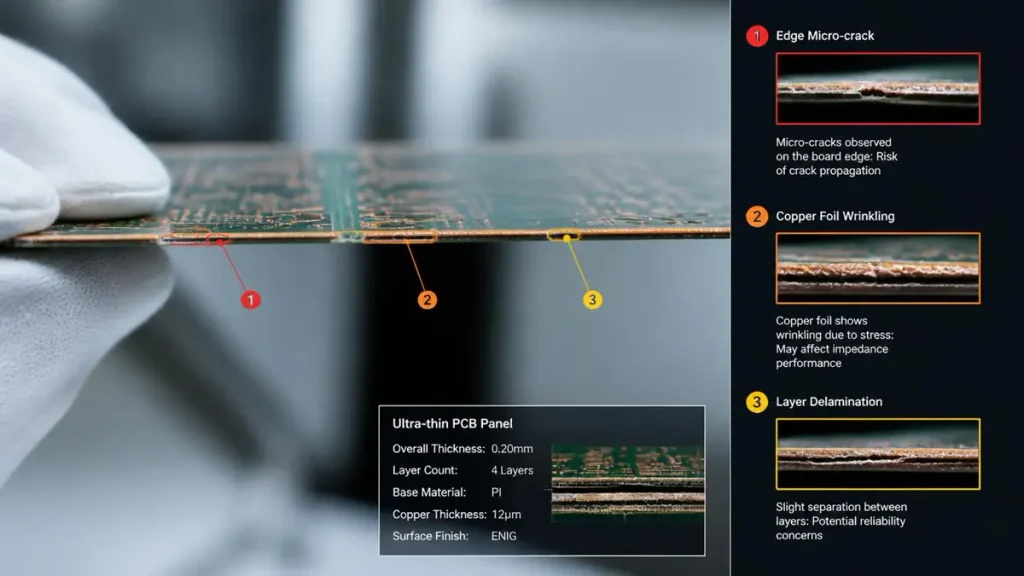
Cross-Sectional Analysis of Common Ultra-Thin PCB Production Defects (0.20 mm Substrate)
If you are sourcing ultra-thin boards, you need to know exactly which thin PCB production defects to look for in first-article inspection reports. Here are the five defect categories that dominate scrap logs.
Cracking, Tearing, and Dents from Improper Handling
This is the most visible and most preventable defect category. Cracks typically originate at panel corners or along V-score lines. Tears happen when thin copper foils catch on conveyor guides or registration pins. Dents and dings are usually caused by manual stacking or contact with hard tooling surfaces. The frustrating part is that these defects often occur after the board has passed electrical test—during depaneling, packaging, or shipping. At our Baoan facility, we use laser depaneling for ultra-thin boards rather than routing or punching, and we ship in vacuum-sealed trays with edge supports. It costs more per panel than bubble wrap, but it eliminates the “mystery damage” that shows up on your receiving dock.
Wrinkles in Ultra-Thin Copper Foil During Lamination
Copper foil wrinkles are a signature defect of thin-core lamination. When prepreg resin flows during hot pressing, it can push unsupported copper into ripples if pressure is applied too quickly or unevenly. Once a wrinkle forms, it creates a permanent topology error that affects solder mask thickness, component placement, and in severe cases, trace continuity. Our LAUFFER lamination system uses programmable pressure ramping and vacuum evacuation before heat application, which allows the prepreg to settle without displacing the copper foil. We also qualify every thin-core material lot for resin flow rate before it enters the clean room.
Delamination Between Copper and Substrate
Ultra thin PCB delamination is the silent killer. It does not show up in visual inspection. It might not even fail initial electrical test. But after a few thermal cycles—say, during your assembly reflow or in the field—it opens into a catastrophic layer separation. The root causes are almost always inadequate surface preparation, moisture absorption in the thin core before lamination, or CTE mismatch between copper and substrate under rapid temperature changes. We address this with plasma desmear for microvia cleaning (which also roughens bonding surfaces at the microscopic level), strict moisture bake protocols for incoming thin materials, and high-Tg FR-4 or BT resin selection for applications that see repeated thermal stress.
Fine-Line Circuit Defects and Etching Non-Uniformity
On ultra-thin boards, trace width variation of ±0.5 mil can shift impedance by 10 %. That is unacceptable for RF or high-speed digital designs. Conventional subtractive etching struggles because the etchant attacks the trace sidewalls as aggressively as the top surface, creating trapezoidal cross-sections. Our mSAP line produces near-vertical trace walls with 8 µm/8 µm line-space capability, which gives designers the routing density they need without sacrificing signal integrity. For thin boards that still run on subtractive processes, we use ultra-low-profile (ULP) copper foil to minimize etch undercut while maintaining peel strength.
How Ultra-Thin PCB Defects Impact Your Project Timeline and Budget
Defects are not just quality issues; they are schedule and budget destroyers. Understanding the cost cascade helps procurement teams justify a higher unit price from a qualified supplier versus a “bargain” quote from a generalist factory.
Scrap Rates That Escalate with Each Processing Stage
A crack in a raw 0.2 mm core is a $3 loss. A crack discovered after laser drilling and electroless copper is a $15 loss. A crack discovered after final ENIG and electrical test is a $40 loss. The later a defect is caught, the more process value it destroys. This is why ultra thin PCB quality control cannot be a final inspection activity; it must be embedded at every stage. Our process includes 100 % 3D AOI after etch, 100 % X-ray inspection after drilling, and microsection analysis on every first-article lot. Catching a delamination tendency at the lamination stage saves the entire downstream investment.
Late-Stage Discovery of Fine-Line Defects
The most expensive defects are the ones your CM discovers during assembly. A fine-line open that passed electrical test but fails under thermal stress will not be found until components are populated and the board is powered. At that point, you are not just scrapping a PCB; you are scrapping components, rework labor, and schedule buffer. We mitigate this with thermal stress testing on first articles—subjecting thin boards to three simulated reflow cycles before final approval—to surface latent defects that would otherwise appear on your SMT line.
Batch-to-Batch Quality Inconsistency in Mass Production
This is the nightmare scenario for procurement: your prototype batch was perfect, but the first production lot has 8 % fallout. Why? Because the prototype was hand-carried by the engineering team, while production ran on standard equipment with standard handling. Thin boards punish process drift more severely than thick boards. A 2 °C temperature variation in the etch bath might be invisible on a 1.6 mm panel, but it can create measurable line-width variation on a 0.2 mm board with 3 mil traces. We control this with automated chemical monitoring, SMEMA-Plus MES integration, and SPC charts on every critical parameter. Our target is not just low defect rates; it is low variation in defect rates from lot to lot.
Shenzhen Hongda Circuit’s Advanced Manufacturing Technology for Thin PCB Yield Improvement
This is where supplier evaluation gets concrete. When you audit a factory for thin PCB manufacturing yield capability, you are really auditing their equipment list and their process discipline. Here is what we have invested in at our Shenzhen facility to make ultra-thin production repeatable.
Laser Direct Imaging (LDI) for Sub-50 µm Trace Precision
Film-based phototools are obsolete for ultra-thin, fine-line work. Film stretches, shrinks with humidity, and degrades after repeated use. Our SCREEN Ledia LDI exposure system writes the resist pattern directly with a UV laser, eliminating phototool error and achieving ±5 µm registration accuracy. For thin boards, this matters because the substrate itself is moving slightly with temperature and humidity; LDI’s real-time fiducial compensation corrects for that movement before each exposure. The result is consistent 3 mil line/space geometry across the entire panel, even on 0.1 mm cores that flex during processing.
Modified Semi-Additive Process (mSAP) for Ultra-Fine Lines
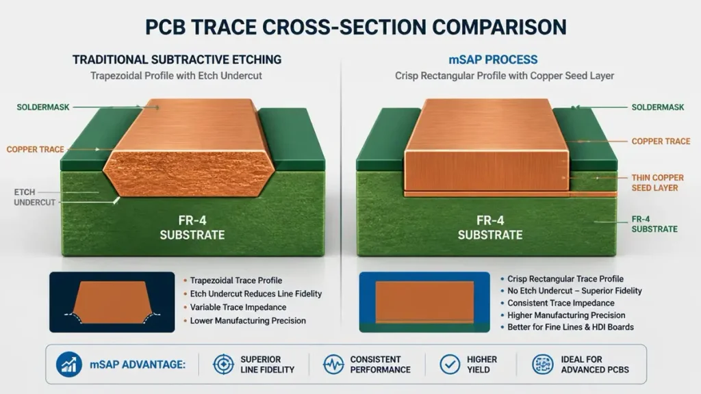
Microscopic Trace Profile Comparison — Traditional Subtractive Etching (Trapezoidal with Etch Undercut) vs. mSAP (Rectangular with Seed Layer)
As mentioned earlier, subtractive etching hits its limit around 3 mil lines on thin copper. Our mSAP line starts with a thin seed layer, plates copper only where traces are needed, and then strips the seed. This creates rectangular trace profiles with minimal undercut, which is critical for controlled impedance on high-speed designs. For ultra-thin HDI boards, mSAP is not a luxury; it is the only way to achieve the routing density that modern chip packages demand without accepting the yield penalty of over-etched traces.
Vacuum Lamination and Low-Pressure Control Systems
Standard hydraulic lamination presses exert 200–350 PSI, which is fine for 1.6 mm multilayers but will crush a 0.2 mm core or squeeze prepreg resin into uneven pools. Our LAUFFER system operates at 150–250 PSI with vacuum evacuation, distributing pressure evenly across the panel surface. We also use thin-core lamination protocols with dedicated buffer materials that absorb resin squeeze-out without creating pressure concentrations at the panel edges. This is where most thin-board delamination starts—at the edges—and our process is specifically tuned to prevent it.
AI-Driven AOI and Zero-Touch Automated Handling
We have eliminated manual panel transfer on our thin-board line. Boards move from loader to LDI to etch to AOI on SMEMA-integrated conveyors with multi-zone vacuum pickup. Our 3D AOI systems use AI-based defect classification to distinguish real defects from false positives, which is critical because thin boards flex slightly under inspection lighting, creating phantom errors that waste engineering time. The AI module learns the specific warpage signature of each panel type and adjusts its judgment thresholds accordingly. This reduces false-call rates by over 35 % compared to rule-based AOI.
Plasma Desmear for Microvia Reliability
In thin HDI boards, microvias are often the only interconnection between layers. If the desmear process leaves resin residue in the hole, plating will be incomplete and the via will fail under thermal stress. We use plasma desmear rather than chemical wet desmear for our ultra-thin line, because plasma removes resin uniformly without swelling the thin substrate or attacking the small-diameter hole walls. The result is >95 % copper coverage in 0.075 mm microvias, verified by cross-section on every production lot.
Our Controlled Process: From Material Management to Final Inspection
Equipment is only half the story. The other half is discipline—the protocols that prevent defects before they happen.
Careful Material Management and Panel Optimization
We receive thin-core materials in vacuum-sealed packaging with humidity indicators. Anything above 30 % RH is baked at 120 °C for four hours before it enters the clean room. We also optimize panelization for mechanical stability: ultra-thin boards are not panelized with aggressive V-scoring that leaves minimal residual thickness. Instead, we use tab-routing with laser depaneling, which preserves edge integrity and eliminates the stress risers that cause corner cracks.
Real-Time Process Monitoring and Closed-Loop Feedback
Every critical machine on our thin-board line is connected to our MES via SMEMA-Plus. Etch bath specific gravity, pH, and temperature are logged every 30 seconds. Lamination pressure and temperature curves are compared to the golden profile for every press cycle. If a parameter drifts outside control limits, the system flags the lot for engineering review before it moves to the next stage. This is how we prevent the “batch-to-batch inconsistency” problem that plagues less automated factories.
Multi-Stage Inspection Protocols for Thin Boards

Automated Optical Inspection (AOI) with Laser Scanning for Ultra-Thin PCB Quality Control
Our inspection sequence for ultra-thin boards includes:
- Incoming material: Thickness, bow/twist, and copper peel strength verification
- Post-drill: 3D X-ray for microvia diameter, position, and aspect ratio
- Post-plate: Cross-section on first article for copper thickness and hole wall quality
- Post-etch: 100 % 3D AOI for line width, spacing, and annular ring integrity
- Post-soldermask: Automated optical inspection for mask dams and registration
- Final: Electrical test with 4-wire Kelvin measurement for high-resistance opens
- Shipping: Vacuum tray packaging with shock indicators
No board ships without passing every gate. It is slower than spot-checking, but for ultra-thin substrates, it is the only way to guarantee reliable ultra thin PCB yield at volume.
What Procurement Teams Should Verify Before Sourcing Ultra-Thin PCBs
If you are evaluating suppliers for a 0.2 mm or thinner project, use this checklist. The answers will tell you whether a factory truly understands ultra thin PCB manufacturing challenges or is simply hoping their standard process will work.
Equipment Capability Checklist for Sub-0.4 mm Production
- Do they have dedicated thin-board handling equipment, or do they run thin panels on standard conveyors?
- Is their imaging system LDI or film-based? (Film is a red flag for sub-3 mil lines.)
- Do they operate vacuum lamination, or standard hydraulic presses?
- Can they show you microsections of 0.075 mm microvias in 0.2 mm substrates?
- Do they have in-house 3D X-ray, or do they outsource inspection?
At PCBkr, we welcome these questions. Our equipment list and capability data are available for verification, and we encourage customer audits.
DFM Review and Early Design Collaboration
The best way to improve ultra thin PCB yield is to design for it from the start. We offer complimentary DFM reviews that specifically address thin-board risks: copper balance for warpage prevention, trace angle optimization to eliminate acid traps, via placement to avoid stress concentrations, and pad sizing to accommodate the registration tolerances of thin substrates. A 20-minute DFM review before layout finalization can eliminate 60 % of potential defects. We return DFM feedback within 24 hours of receiving your Gerber and stackup.
Certifications and Track Record in High-Mix Thin Board Orders
Paper claims are easy; production history is hard. Ask for:
- ISO 9001:2015 (minimum)
- IPC-6012 Class 3 or 3A for high-reliability applications
- IATF 16949 if you are in automotive
- ISO 13485 for medical
- Actual yield data from thin-board production lots (not just overall factory yield)
Shenzhen Hongda Circuit Technology maintains ISO 9001, AS9100D (aerospace), IATF 16949 (automotive), and ISO 13485 (medical) certifications. Our thin-board line has shipped over 500,000 panels in the 0.1 mm–0.4 mm range since 2022, with documented yield trends that we share under NDA during supplier qualification.
Achieving Reliable Ultra-Thin PCB Yield with Hongda Circuit
Ultra-thin PCB manufacturing is not about doing the same things more carefully. It is about using different equipment, different processes, and different handling protocols because the physics of thin substrates are fundamentally unforgiving. The factories that treat 0.2 mm boards as “just thinner 1.6 mm boards” are the ones that deliver 70 % yields and blame the material.
At Shenzhen Hongda Circuit Technology Co., Ltd., we built our thin-board line from the ground up with mSAP imaging, vacuum lamination, zero-touch handling, and AI-enhanced inspection. We do not subcontract thin-core lamination or microvia drilling. Every process step is in-house, traceable, and monitored in real time. That is how we deliver thin PCB manufacturing yield that meets your production schedule, not just your prototype demo.
Ready to evaluate your ultra-thin PCB project?
Submit your Gerber files, stackup requirements, and target thickness to sales@pcbkr.com. Our engineering team will return a complimentary DFM review, process capability assessment, and detailed quotation within 30 minutes.
Shenzhen Hongda Circuit Technology Co., Ltd.
Room 1608-1610, Research Development Comprehensive Building, Baoyunda Logistics Center, Baoan, Shenzhen, China
📧 sales@pcbkr.com | pcb@pcbkr.com
📞 +86 0755 23720053
🌐 www.pcbkr.com
FAQ: Ultra-Thin PCB Sourcing from a Buyer’s Perspective
What is the typical thin PCB manufacturing yield for 0.2 mm boards, and how does it compare to standard 1.6 mm PCBs?
Thin PCB manufacturing yield for 0.2 mm boards typically runs 85–92 % at qualified factories, compared to 96–99 % for standard 1.6 mm boards. The gap comes from handling damage, lamination warpage, and fine-line etch variation. At PCBkr, we target >95 % first-pass yield on 0.2 mm single-sided and >90 % on multilayer thin HDI through vacuum lamination, LDI imaging, and zero-touch handling. Always ask for yield data by thickness range, not just overall factory averages.
What are the most common ultra thin PCB defects I should inspect for during first-article approval?
The five critical ultra thin PCB defects to verify are: (1) corner cracks and edge tears from mechanical handling; (2) copper foil wrinkles from uneven lamination pressure; (3) delamination at layer interfaces, visible in microsection; (4) fine-line opens or shorts from etch undercut; and (5) microvia plating voids or incomplete copper coverage. Request cross-section photos, 3D AOI scan data, and thermal stress test results with your first article.
How can I improve ultra thin PCB yield before the factory even starts production?
The fastest way to improve yield is early DFM collaboration. At PCBkr, we review your design for copper balance (to prevent warpage), trace angles (to eliminate acid traps), and via placement (to reduce stress concentrations). We also recommend material selection—high-Tg FR-4 or BT resin for thermal cycling, ULP copper for fine-line etching. A 24-hour DFM review can eliminate 60 % of potential defects before tooling begins.
What equipment should I verify when auditing a supplier for thin PCB production defects control?
Verify five capabilities: (1) Laser Direct Imaging (LDI) for sub-50 µm registration—film-based imaging is insufficient; (2) vacuum lamination with programmable pressure, not standard hydraulic presses; (3) plasma desmear for microvia cleaning in thin substrates; (4) 3D X-ray inspection for microvia and buried via verification; and (5) zero-touch vacuum handling rather than mechanical edge grippers. Missing any of these increases your risk of thin PCB production defects significantly.
Why does ultra thin PCB delamination happen, and how do you prevent it?
Ultra thin PCB delamination is caused by moisture in the core before lamination, inadequate surface roughness for copper adhesion, or CTE mismatch during thermal cycling. We prevent it with three controls: strict incoming material baking (<30 % RH threshold), plasma desmear that creates microscopic bonding anchors without swelling the substrate, and high-Tg material selection for applications with repeated thermal stress. Every production lot undergoes thermal shock testing (10 cycles, -65 °C to +150 °C) to verify layer adhesion before shipment.
About Author
David Chen https://www.linkedin.com/in/pcbcoming
David Chen boasts an extensive professional background in PCBA manufacturing, PCBA testing, and PCBA optimization, with specialized expertise in high-precision PCBA fault analysis and rigorous PCBA reliability testing. The author has worked with high-layer-count server PCB fabrication, ultra-low-loss backplane stackups, and thermo-mechanical reliability optimization for AI infrastructure projects involving 112G and 224G PAM4 architectures. Skilled in complex circuit design and cutting-edge advanced PCB manufacturing processes, he delivers solutions that elevate product durability and performance across industrial applications. His technical articles focusing on PCBA manufacturing workflows and testing methodologies are widely cited by industry peers, research institutions, and technical platforms, solidifying his reputation as a recognized technical authority in the global circuit board manufacturing sector.