Ultra-Thin PCB for Automotive Electronics: A Procurement Guide for OEM & Tier-1 Buyers
Every gram and every millimeter counts in modern vehicle design. As ADAS cameras shrink into wing-mirror housings, as infotainment displays curve around dashboard contours, and as battery management systems pack monitoring electronics into gaps between cells, the interconnect platform underneath those components has become a critical bottleneck. Standard 1.6 mm multilayer boards simply do not fit anymore. This is why procurement teams at automotive OEMs and Tier-1 suppliers are increasingly sourcing ultra thin automotive PCB solutions — not as a niche option, but as a standard requirement for next-generation vehicle platforms.
At Shenzhen Hongda Circuit Technology Co., Ltd., we fabricate thin PCB for automotive electronics ranging from 0.1 mm flexible circuits to 0.4 mm rigid HDI boards, shipping to ADAS module makers, EV powertrain integrators, and cockpit display manufacturers across North America, Europe, and Asia. This guide is written for the engineer or procurement manager who needs to qualify a supplier, evaluate stack-up options, and de-risk a program before the first prototype order is placed.
What Is an Ultra-Thin Automotive PCB and Why Does It Matter for Modern Vehicle Design?
Defining Ultra-Thin PCB Thickness Ranges for Automotive Applications
There is no universal industry standard that draws a hard line between “standard” and ultra-thin PCB automotive products, but in our Shenzhen facility and across the Tier-1 supply base, the consensus threshold sits at 0.5 mm total board thickness. Boards below this mark — commonly 0.4 mm, 0.3 mm, and in extreme flex cases down to 0.1 mm — are classified as ultra-thin. These thicknesses are achieved through a combination of thin-core dielectrics (often 0.05 mm to 0.1 mm prepreg or core), reduced copper weights, and sequential lamination processes that maintain layer registration without adding excessive resin bulk.
The automotive flexible PCB segment pushes these boundaries further. Polyimide-based flex circuits used in steering-wheel controls, seat sensors, and LED ambient lighting can be manufactured at 0.1 mm to 0.2 mm while retaining dynamic bend capability across 10,000+ cycles.
The Role of Thin PCB Technology in ADAS, Infotainment, and EV Control Modules
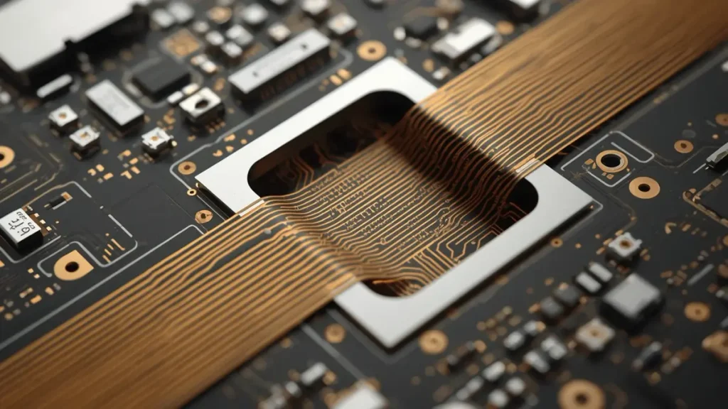
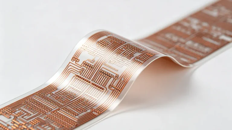
Ultra-Thin Flexible PCB (FPC) Integrated in ADAS Camera Module – Hongda Circuit
The shift toward electrification and autonomy is the primary demand driver. Modern vehicles now integrate multiple radar, camera, ultrasonic, and lidar sensors feeding domain controllers that require complex, high-layer-count PCBs
. In these systems, thin PCB for automotive electronics serves three simultaneous functions:
- Mechanical fit: A 0.3 mm rigid board slides into a camera housing where a 1.2 mm board would require a complete housing redesign.
- Signal integrity: Shorter via stubs and reduced dielectric thickness improve impedance control for 77 GHz radar and high-speed LVDS camera links.
- Weight reduction: In a premium EV where 50+ PCBs are distributed across the vehicle, cutting 30–40% of interconnect mass contributes directly to range optimization.
Key Pain Points Solved by Ultra-Thin PCB Solutions in Automotive Electronics
Space Constraints and Weight Reduction in Compact Automotive Assemblies
The most immediate pain point is physical. Tier-1 suppliers frequently approach us with a finished mechanical design — a folded headlamp assembly, a curved center console, or a slim door module — only to discover that the allocated PCB cavity leaves less than 0.6 mm of vertical space. A low profile PCB automotive OEM specification in this scenario is not negotiable; it is a boundary condition. Ultra-thin boards eliminate the need for mechanical compromises such as external connector boxes or split-board cable harnesses.
Signal Integrity Challenges in High-Frequency Automotive Radar and Camera Systems
ADAS modules operating at millimeter-wave frequencies (24 GHz, 77–81 GHz) are unforgiving. Dielectric thickness directly impacts stripline and microstrip impedance. On a standard 1.6 mm board, maintaining 50 Ω or 100 Ω differential pairs with tight coupling often requires impossibly wide traces or exotic material costs. By dropping to a 0.3 mm or 0.4 mm stack-up with thin-core Rogers or Panasonic Megtron 6, engineers regain trace-width flexibility and reduce insertion loss. Our engineering team routinely runs TDR verification on these stack-ups before laser drilling begins, ensuring that impedance targets survive the transition from simulation to fabrication.
Thermal Management and Vibration Resistance in Thin Profile PCBs
A common misconception is that thinner boards run hotter. While reduced copper mass does lower thermal capacitance, the real thermal bottleneck in automotive modules is usually the interface between the PCB and its housing, not the board itself. We address this through thermal via farming — placing 0.2 mm microvia arrays under QFN and DFN power devices — and by specifying high-Tg FR-4 (Tg ≥ 170 °C) or ceramic-filled hydrocarbon materials that maintain thermal conductivity even at reduced thickness. For vibration, automotive flexible PCB sections absorb mechanical stress in rigid-flex assemblies, preventing solder-joint fatigue in modules mounted near engines or suspension systems.
Ultra-Thin Rigid, Flexible, and Rigid-Flex PCB Options for Automotive Use
When to Specify Ultra-Thin Rigid PCB for Automotive Control Units
Ultra-thin rigid PCB remains the workhorse for ECUs, BMS monitoring boards, and LED driver modules where the assembly is fixed in a flat plane but vertical clearance is minimal. We typically see these specifications in 4-layer to 10-layer builds at 0.4 mm to 0.5 mm total thickness, using thin-core FR-4 with 1/2 oz or 1/3 oz copper to maintain etch precision. The advantage of rigid ultra-thin boards is straightforward: they process through standard SMT lines with minimal handling protocol changes, yet deliver the space savings the mechanical team demands.
Automotive Flexible PCB Applications in Dynamic and Tight-Space Environments
Automotive flexible PCB — built on polyimide (PI) or liquid crystal polymer (LCP) — is specified when the interconnect must bend, fold, or twist during assembly or operation. Typical automotive flex applications include:
- Around-shaft sensors: Flex circuits wrapping steering columns with bend radii below 3 mm.
- Seat occupancy sensors: Large-area flex mats that conform to foam contours.
- Foldable display hinges: Dynamic flex circuits in emerging foldable cockpit concepts.
At Hongda Circuit, our flex lines handle 1-layer to 6-layer builds with coverlay openings for component pads and stiffener bonding (PI, FR-4, or stainless steel) for localized rigidity where connectors are mounted.
Rigid-Flex PCB Hybrid Solutions for Multi-Zone Automotive Modules
Rigid-flex PCB bridges the gap. A single part number can incorporate rigid mounting zones for ICs and connectors, connected by flexible “arms” that route signals across hinge lines or around corners. This eliminates separate board-to-board connectors, reduces assembly labor, and improves reliability under the thermal cycling and vibration loads defined in IEC 60068-2-6 and IEC 60068-2-14. For automotive programs, we recommend rigid-flex when the module has three or more rigid islands that would otherwise require FPC cables or wire harnesses.
Technical Specifications Buyers Must Verify When Sourcing Thin PCB for Automotive Electronics
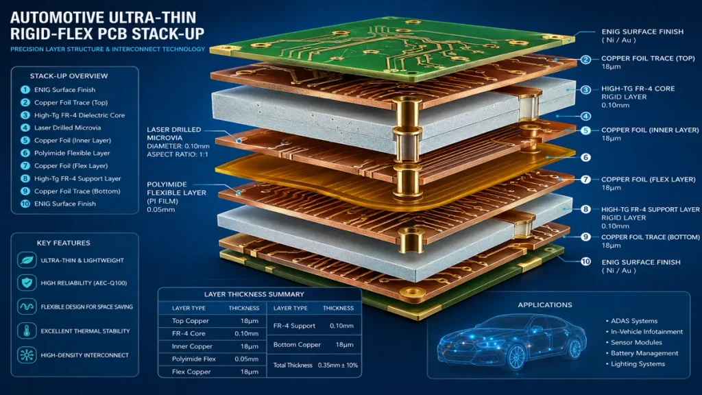
3D Layer Stack-Up Diagram of Ultra-Thin Automotive Rigid-Flex PCB – Hongda Circuit
Layer Count, Microvia Capability, and Minimum Line Width/Spacing
Before issuing an RFQ, verify that the supplier’s capability table aligns with your design rules. For ultra thin automotive PCB programs, the critical parameters are:
| Parameter | Typical Automotive Requirement | Hongda Circuit Capability |
|---|---|---|
| Minimum trace width/space | 3 mil / 3 mil (HDI) | 2.5 mil / 2.5 mil |
| Microvia diameter | 4 mil (100 μm) | 3 mil (75 μm) |
| Aspect ratio (microvia) | ≤ 0.8:1 | ≤ 1:1 |
| Layer count (thin rigid) | 4–10 layers | Up to 12 layers at 0.4 mm |
| Total thickness (rigid) | 0.3–0.5 mm | 0.2–0.6 mm |
| Total thickness (flex) | 0.1–0.2 mm | 0.08–0.25 mm |
These numbers matter because ultra thin HDI PCB for ADAS designs often pack 0.4 mm pitch BGA devices or 0201 passives into areas smaller than a postage stamp. A supplier advertising “HDI capability” but lacking controlled laser drilling and sequential lamination experience will struggle with yield on these builds.
Controlled Impedance and High-Frequency Material Options
Radar and high-speed camera links demand controlled impedance within ±10%. We validate every automotive stack-up with polar TDR measurement and provide a report with the first article. For 77 GHz radar front ends, we specify low-Dk materials such as Rogers RO3003 (εr = 3.0, Df = 0.0013) or Taconic TLY-5, bonded to thin FR-4 cores for mechanical stability. The key procurement question is not just “can you buy Rogers?” but “can you control dielectric thickness within ±0.01 mm across a 500 mm panel after sequential lamination?” That is where process discipline separates qualified automotive suppliers from trading companies.
Surface Finish Selection for Automotive SMT Reliability
For fine-pitch QFN and BGA assembly on thin boards, ENIG (Electroless Nickel Immersion Gold) remains the default. However, for modules subject to high-temperature underhood operation or where shelf life exceeds 12 months, we also recommend ENEPIG (Electroless Nickel Electroless Palladium Immersion Gold) or Immersion Silver for its flatness and excellent solderability. OSP is generally avoided in automotive unless the assembly house has nitrogen reflow and extremely tight process control, because thin boards warp more easily during thermal profiling, and OSP’s single-reflow protection window is narrow.
Material Science and Stack-Up Design for High-Reliability Thin Automotive PCBs
Thin Core FR-4 vs. Polyimide: Matching Substrate to Application
The substrate choice is the single most consequential decision in an ultra-thin PCB automotive program. Our material lab evaluates each project against this matrix:
- Thin-core FR-4 (High Tg, 170 °C+): Specified for rigid ultra-thin boards in underhood or powertrain modules. It offers cost efficiency, mature supply chains, and compatibility with standard PCB processing. The trade-off is limited flexibility and higher Dk (~4.3–4.5).
- Polyimide (PI, 25 μm–50 μm): The standard for automotive flexible PCB and rigid-flex flex layers. It survives -40 °C to +125 °C continuous operation, maintains dielectric strength after 10,000 flex cycles, and bonds reliably with acrylic or epoxy-based coverlay films.
- LCP (Liquid Crystal Polymer): Emerging for 5G automotive antennas and 77 GHz radar feedlines due to its ultra-low moisture absorption (< 0.04%) and stable Dk across temperature. Higher cost, but justified when signal integrity is paramount.
Low-Dk Materials for Millimeter-Wave Radar and 77 GHz Automotive Sensors
Millimeter-wave radar modules cannot tolerate dielectric constant variation. A 0.1 mm shift in prepreg thickness can detune an antenna array. For these programs, we engineer hybrid stack-ups: a thin Rogers or Taconic core for the RF layer, bonded to standard FR-4 for digital routing layers. The lamination pressure and temperature profile are tightly controlled to prevent resin starvation or excessive flow that would alter the final dielectric thickness.
Copper Weight, Dielectric Thickness, and Total Stack-Up Optimization
On ultra-thin boards, copper weight is a double-edged sword. Heavier copper (2 oz, 3 oz) improves current capacity and thermal spreading but makes etching fine lines nearly impossible and increases overall stiffness. For most thin PCB for automotive electronics applications, we specify:
- Signal layers: 1/3 oz or 1/2 oz copper, allowing 2.5 mil lines.
- Power layers: 1 oz copper, with thermal via arrays under hot spots.
- Outer layers: 1/2 oz base + 20 μm plating, providing enough copper for reliable microvia plating without over-etching fine traces.
The total stack-up is modeled in Polar Si9000 or similar field solvers before CAM work begins, ensuring that impedance, insertion loss, and crosstalk targets are met with margin.
Manufacturing Excellence: Advanced Equipment and Process Control at Shenzhen Hongda Circuit
Laser Drilling and Sequential Lamination for HDI Thin PCB Production
The heart of any ultra thin HDI PCB for ADAS facility is its laser drilling capability. At Hongda Circuit, we operate UV laser drilling systems capable of producing 75 μm microvias with positional accuracy within ±12 μm. The laser process is not merely about hole size; it is about controlling the energy profile to prevent carbonization of the dielectric, ensuring clean via walls that accept electroless copper without voids
Sequential lamination follows. Each sub-composite is laser-drilled, plated, and inspected before the next lamination cycle. This “build-up” approach enables 2+N+2 and 3+N+3 HDI structures in total thicknesses below 0.5 mm — a requirement for modern zonal automotive controllers that aggregate data from multiple sensors onto a single compact board.
Automated Optical Inspection (AOI) and 100% Electrical Testing Protocols
Defect detection on thin boards is harder than on standard boards because warpage can cause false calls in automated systems. We address this with 3D AOI on inner layers, using height-map algorithms to distinguish true defects from board bow. Every automotive panel undergoes:
- Flying probe testing for prototypes and small batches (100% netlist verification).
- Grid testing for volume production.
- 4-wire Kelvin testing on microvia chains to detect intermittent opens caused by micro-fractures.
Warpage Control and Plating Uniformity in Ultra-Thin Board Fabrication
Warpage is the silent killer of ultra-thin PCB yield. Boards that bow beyond 0.75% after reflow simulation will jam in SMT lines or create solder joint defects. We control this through:
- Symmetric stack-up design: Mirroring copper weights and layer densities around the board’s neutral axis.
- Controlled cool-down profiles in lamination presses, avoiding thermal shock that locks in stress.
- Panel plating with pulse rectifiers: Achieving ±8% copper thickness uniformity across the panel, even on 0.3 mm thin cores where current density variations are magnified.
IATF 16949, IPC Class 3, and Automotive Compliance: Non-Negotiable Supplier Criteria
Why IATF 16949 Certification Is the Minimum Threshold for Automotive PCB Procurement
If a supplier cannot produce a current IATF 16949 certificate covering the exact manufacturing site (not just a sales office), disqualify them immediately. This is not procurement rigidity; it is risk management. IATF 16949 mandates the use of core quality tools — APQP, PPAP, FMEA, SPC, and MSA — that are structurally absent from ISO 9001-only facilities
At Hongda Circuit, our IATF 16949 system is audited annually and covers our full Shenzhen fabrication campus. We maintain Level 3 PPAP documentation for active automotive programs, including dimensional results, material certifications, and process capability studies (Cpk ≥ 1.67 for critical dimensions).
IPC-6012 and IPC-6013 Standards for Rigid and Flexible Automotive Circuits
Beyond IATF, the product itself must meet automotive-grade IPC standards:
- IPC-6012DA (Automotive Addendum to IPC-6012): Tighter tolerances on conductor width, plating thickness, and solder mask adhesion than base IPC-6012 .
- IPC-6013: Qualification and performance specification for flexible and rigid-flex printed boards, defining bend testing, coverlay adhesion, and dynamic flex requirements.
We build to IPC Class 3 as standard for automotive, with Class 3A (high-reliability) available on request for safety-critical brake-by-wire or steer-by-wire modules.
Traceability, Batch Control, and PPAP Documentation Support
Automotive OEMs require lot-level traceability from raw material to finished board. Our ERP system links every PCB serial number to:
- Laminate lot numbers and UL recognition files.
- Drill bit and plating bath records.
- AOI and electrical test logs.
- Outgoing inspection data and packing list.
This traceability is not an afterthought; it is embedded in our IATF work instructions. When a Tier-1 customer initiates a field failure analysis, we can pull the complete manufacturing pedigree within 24 hours.
Procurement Strategy: Evaluating Ultra-Thin Automotive PCB Suppliers Beyond Price
DFM Engagement and Early-Stage Engineering Support
The cheapest quote is often the most expensive mistake. A qualified automotive rigid flex PCB supplier should offer DFM feedback before you freeze the Gerber. At Hongda Circuit, our engineering review process flags issues such as:
- Microvia aspect ratios that exceed reliable plating limits.
- Copper-to-edge distances that risk burr formation during routing.
- Stiffener placements that interfere with dynamic flex regions.
- Impedance stack-ups that require material lead times beyond your program schedule.
This review typically turns around in 48 hours and has saved customers from respins that would have cost weeks and tens of thousands of dollars.
Prototype Lead Time and Quick-Turn Capabilities for Automotive NPI
New product introduction (NPI) in automotive moves on aggressive timelines. We maintain a dedicated quick-turn line for automotive prototypes, delivering:
- 2-layer to 6-layer ultra-thin rigid: 5–7 days.
- 8-layer to 10-layer HDI thin boards: 10–12 days.
- Rigid-flex and flex prototypes: 7–10 days.
These lead times include in-house impedance testing and cross-section analysis, so the first article you receive is a validated article, not a guess.
Scalability from Low-Volume Validation to High-Volume Mass Production
The real procurement risk is not the prototype; it is the ramp. Many suppliers excel at 50-piece prototypes but collapse at 5,000-piece monthly volumes due to plating bath capacity or lamination press bottlenecks. Our Shenzhen facility operates with a monthly output capacity that scales from pilot runs to mass production without requiring a second supplier qualification — a critical advantage for automotive programs where PPAP re-qualification can take 12–16 weeks.
Frequently Asked Questions by Automotive PCB Buyers
How thin can automotive PCBs be manufactured without sacrificing reliability?
For rigid automotive boards, 0.2 mm to 0.3 mm is the practical floor for multi-layer builds that must survive IPC-6012 thermal stress testing and SMT reflow. Below 0.2 mm, handling damage during assembly becomes the dominant failure mode. For automotive flexible PCB applications, 0.08 mm to 0.1 mm is routine for single-layer flex, and 0.15 mm to 0.2 mm for 2-layer dynamic flex. Reliability is maintained by specifying high-Tg materials, symmetric stack-ups, and conservative bend radii (minimum 10× thickness for dynamic flex).
What is the difference between ultra-thin PCB and standard PCB for automotive use?
The difference is more than thickness. A standard PCB (1.0 mm to 1.6 mm) offers easier handling, lower raw material cost, and greater tolerance for mechanical drilling. An ultra-thin PCB automotive build (≤ 0.5 mm) requires laser drilling for microvias, sequential lamination for layer registration, and specialized fixturing to prevent warpage during plating and etching. The procurement implication is that not every PCB factory can reliably produce ultra-thin automotive volumes — the equipment set and process control discipline are fundamentally different.
Which surface finish is best for fine-pitch automotive SMT on thin boards?
ENIG is the safest default for fine-pitch QFN and BGA assembly on thin boards because of its flatness and long shelf life. However, for modules operating above 125 °C ambient or requiring wire bonding, ENEPIG is superior due to its palladium barrier layer preventing nickel corrosion. Immersion Silver is a viable cost-optimized alternative for high-volume, short-shelf-life programs with nitrogen reflow capability. HASL is generally avoided in automotive fine-pitch applications because of thickness variation and planarity issues.
How do I verify that a PCB supplier is truly IATF 16949 qualified, not just ISO 9001?
Request three specific documents: (1) the IATF 16949 certificate itself, verifying the certification body (e.g., SGS, TÜV, Bureau Veritas) and ensuring the scope covers the manufacturing site address, not a sales office; (2) a sample PPAP Level 3 submission from a recent automotive program, proving they actually use APQP and FMEA in practice; and (3) a lot traceability report showing material-to-finished-goods linkage. ISO 9001 alone is insufficient for automotive supply
What material should I specify for a thin automotive flexible PCB in a high-vibration environment?
Specify polyimide (PI) with acrylic adhesive for standard -40 °C to +105 °C applications, or adhesiveless PI for higher reliability and thinner profiles. If the flex circuit will experience continuous dynamic bending (e.g., steering column or seat track), specify rolled-annealed (RA) copper rather than electrodeposited (ED) copper, as RA copper’s grain structure withstands fatigue far better. For chemical resistance (underhood exposure), consider LCP (Liquid Crystal Polymer) instead of PI, though at a 20–30% cost premium.
Ready to Qualify Your Ultra-Thin Automotive PCB Supplier?
Shenzhen Hongda Circuit Technology Co., Ltd. builds ultra thin automotive PCB, automotive flexible PCB, and rigid-flex PCB solutions for ADAS, EV powertrain, and cockpit electronics programs. From DFM review and impedance-matched stack-up design to IATF 16949-controlled mass production, we support OEM and Tier-1 procurement teams through every phase of the automotive NPI cycle.
Submit your Gerber, stack-up requirements, and environmental conditions today for a DFM review and detailed quotation.
📧 Email: sales@pcbkr.com
🌐 Website: www.pcbkr.com
📍 Facility: Shenzhen, China — IATF 16949 certified, IPC Class 3, full lot traceability.
About Author
David Chen https://www.linkedin.com/in/pcbcoming
David Chen boasts an extensive professional background in PCBA manufacturing, PCBA testing, and PCBA optimization, with specialized expertise in high-precision PCBA fault analysis and rigorous PCBA reliability testing. The author has worked with high-layer-count server PCB fabrication, ultra-low-loss backplane stackups, and thermo-mechanical reliability optimization for AI infrastructure projects involving 112G and 224G PAM4 architectures. Skilled in complex circuit design and cutting-edge advanced PCB manufacturing processes, he delivers solutions that elevate product durability and performance across industrial applications. His technical articles focusing on PCBA manufacturing workflows and testing methodologies are widely cited by industry peers, research institutions, and technical platforms, solidifying his reputation as a recognized technical authority in the global circuit board manufacturing sector.