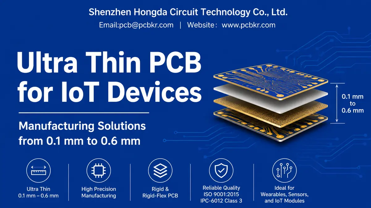
Ultra Thin PCB for IoT Devices: Manufacturing Solutions from 0.1 mm to 0.6 mm
Ultra Thin PCB for IoT Devices — When Every Micron Determines Product Market Fit
Your IoT product concept is solid. The firmware team has the stack optimized. The industrial designer has sketched a housing that looks like it belongs on a retail shelf. Then the mechanical engineer drops the bomb: the internal Z-height budget leaves less than 0.5 mm for the PCB.
That is not a edge case. That is the new normal.
At Shenzhen Hongda Circuit Technology Co., Ltd. (PCBKR), we manufacture ultra thin PCB for IoT devices starting at 0.1 mm finished thickness — not as a one-off lab sample, but as a repeatable, ISO 9001:2015 / IPC-6012 Class 3 production reality. Our Bao’an facility runs a dedicated thin-board production lane with SCREEN Ledia LDI direct imaging, Mitsubishi UV/CO₂ hybrid laser drilling, and LAUFFER controlled-pressure lamination systems specifically configured for low-profile substrates. We have shipped ultra thin rigid PCB and ultra thin rigid-flex PCB assemblies into wearable health monitors, Sub-GHz asset trackers, BLE sensor nodes, and 5G IoT gateway modules.
This page is written for the procurement team that is tired of capability sheets that promise everything and prove nothing. We will walk through what ultra thin PCB manufacturing actually requires, where most suppliers cut corners, and how our 2026-spec process stack solves the three failure modes that kill IoT programs: warpage during SMT, impedance drift after reflow, and microvia fracture under thermal cycling.
What Is an Ultra Thin PCB for IoT? Definitions That Actually Matter on the Factory Floor
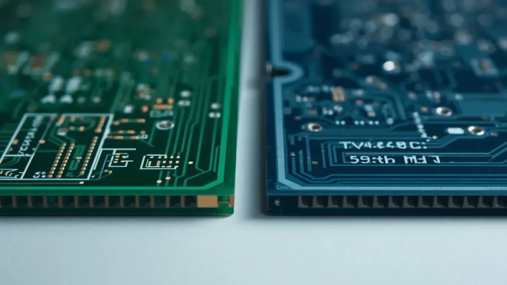
Ultra Thin PCB (0.1mm) vs Standard PCB (1.6mm) Thickness Comparison
Ultra Thin PCB Thickness Range — Why 0.1 mm to 0.4 mm Is the IoT Sweet Spot
Industry literature often throws around “thin PCB” without defining it. Here is how we segment it at PCBKR, based on what our SMT partners can reliably assemble:
| Category | Finished Thickness | Typical IoT Application |
|---|---|---|
| Standard PCB | 1.0 mm – 1.6 mm | General control boards, legacy industrial IoT |
| Thin PCB | 0.5 mm – 0.8 mm | Compact Wi-Fi modules, smart home hubs |
| Ultra Thin PCB | 0.1 mm – 0.4 mm | Wearables, medical patches, asset tags, earables |
| Extreme Ultra Thin | < 0.1 mm | Disposable NFC sensors, paper-thin RFID inlays |
For IoT hardware, the 0.1 mm – 0.4 mm band is where the real engineering trade-offs live. At 0.3 mm, you can still run a 4-layer FR-4 stack with controlled impedance and standard 0201 SMT placement. Push below 0.2 mm, and you are typically looking at polyimide (PI) cores, modified epoxy systems, or hybrid rigid-flex constructions with localized stiffeners.
The distinction matters because not every factory that claims “ultra thin PCB capability” has solved the lamination pressure problem. Standard hydraulic presses apply uniform tonnage across the panel. On a 0.2 mm core, that pressure crushes resin flow channels and creates resin-starved zones that later fracture under vibration. Our LAUFFER lamination system uses zone-controlled pressure profiling — we dial back tonnage by 18–22 % on sub-0.4 mm panels compared to standard 1.6 mm jobs. That sounds like a minor tweak, but it is the difference between a board that survives 1,000 thermal cycles and one that delaminates at 200.
Ultra Thin PCB vs. Standard PCB — A Procurement Checklist
If you are evaluating an ultra thin PCB manufacturer for the first time, do not accept a generic capability matrix. Ask for these specifics:
- Core thickness tolerance: We hold ±0.03 mm on 0.2 mm cores. Some shops quote ±0.05 mm and hope you will not measure.
- Post-etch copper thickness: On 1/2 oz base copper, our post-etch target is 12.5 µm ±1.5 µm. Variation here directly impacts RF trace impedance.
- Warpage post-reflow: We guarantee < 0.5 % bow and twist on panels up to 250 mm × 300 mm after three simulated reflow cycles. Ask for the test coupon.
- Microvia aspect ratio: For 0.1 mm blind vias in 0.2 mm total thickness, the aspect ratio is 2:1. That is aggressive but manageable with our Mitsubishi UV laser. A CO₂-only shop will struggle.
Why IoT Product Teams Specifically Need Ultra Thin PCB Solutions
The Z-Height Crisis in Wearable IoT and Medical Sensors
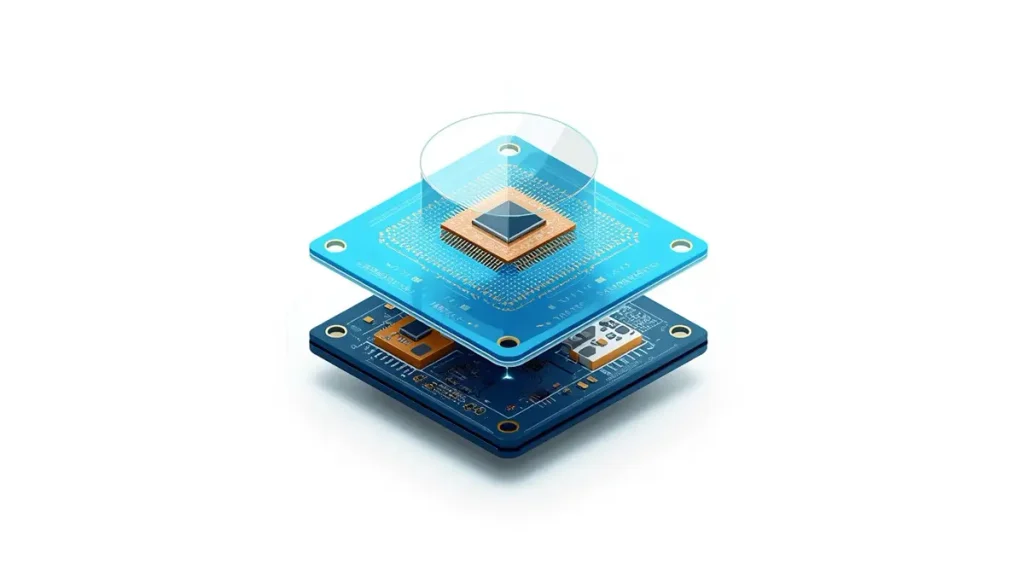
3D Exploded View of Ultra Thin PCB Stackup for Wearable Medical Sensors
IoT devices are not just getting smaller; they are getting flatter. A smart ring has maybe 4 mm of internal height. Subtract 1.5 mm for the battery, 0.8 mm for the optical sensor stack, 0.5 mm for the housing wall, and you have 1.2 mm left for electronics. If your PCB is 1.0 mm, you have 0.2 mm for components. Good luck fitting a MEMS accelerometer and a Bluetooth SoC in that envelope.
An ultra thin PCB for wearable devices solves this by giving the mechanical designer headroom. We have shipped 0.25 mm 4-layer boards for a European client’s continuous glucose monitor patch. The board itself is thinner than a credit card, yet it carries a 50 Ω single-ended RF trace to a ceramic chip antenna, a 100 Ω differential pair for the SPI bus, and a dedicated ground plane to shield the analog front end from the DC-DC switching noise.
Weight Reduction for Drone-Mounted and Portable IoT Hardware
Every gram matters in logistics trackers that ride on high-value pharmaceutical shipments. A standard 1.6 mm FR-4 board for a LoRaWAN node might weigh 8–12 grams. Our 0.3 mm ultra thin FR-4 equivalent drops that to 3–4 grams. When you are paying air freight by the kilogram and deploying 10,000 units, that delta is not trivial.
Space for Battery and Antenna — The Real IoT Design Constraint
Engineers often assume the PCB is the limiting factor. It is not. The battery and the antenna are. An ultra thin PCB stackup design lets you place the PCB in the same plane as a flexible printed battery or wrap a polyimide antenna around the housing interior. We recently collaborated on a smart label project where the 0.15 mm PCB, the 0.2 mm printed battery, and the 0.1 mm NFC antenna coil were laminated into a single 0.6 mm assembly. That is not a board. That is a system substrate.
Ultra Thin PCB Specifications and Material Stackups for IoT Applications
Material Selection — FR-4, Polyimide, and Low-Loss Laminates
Not all ultra thin PCB substrates are created equal. Here is what we stock and qualify for IoT work:
FR-4 (Modified Thin-Core)
- Thickness: 0.1 mm, 0.15 mm, 0.2 mm cores available
- Tg: 150 °C standard, 170 °C high-Tg option for lead-free reflow
- Best for: Cost-sensitive BLE modules, environmental sensors, smart home devices
- Limitation: Dk ~4.4 @ 1 GHz. Fine for 2.4 GHz ISM band, but lossy above 6 GHz.
Polyimide (PI) — DuPont Kapton® / Equivalent
- Thickness: 0.025 mm, 0.05 mm, 0.075 mm, 0.125 mm
- Tg: > 300 °C
- Best for: Flexible or rigid-flex IoT wearables, medical patches, curved surface mounting
- Advantage: Dk ~3.4, lower loss than FR-4. Bends to a 1 mm radius without copper fracture on 1/2 oz traces.
Low-Loss Laminates — Rogers RO4000® Series, Taconic TLY®, M9-Grade CCL
- Thickness: 0.1 mm – 0.254 mm
- Dk: 2.2 – 3.5 @ 10 GHz
- Df: 0.0005 – 0.002 @ 10 GHz
- Best for: 5G IoT modules, mmWave sensor arrays, high-frequency RFID readers
- Reality check: These materials cost 3–5× standard FR-4. We only recommend them when the RF link budget genuinely requires it. For a Sub-GHz LoRa node, low-loss laminate is overkill and burns BOM margin.
Copper Weight and Trace Density on Ultra Thin Substrates
On a 0.2 mm total thickness board, you cannot bury 2 oz copper in the core and expect the prepreg to flow evenly. Our standard IoT stack uses 1/2 oz (17.5 µm) or 1 oz (35 µm) base copper on all layers. For power-hungry IoT gateways that need heavier copper, we use external 2 oz with 0.5 mm trace width rather than thick inner layers, which keeps the core thin while managing I²R loss.
Trace/space capability:
- Mass production: 3 mil / 3 mil (0.075 mm / 0.075 mm)
- Prototype / mSAP lane: 1.0 mil / 1.0 mil (0.025 mm / 0.025 mm)
The 1 mil capability runs on our mSAP (modified semi-additive process) line, which is overkill for most IoT sensors but essential if you are routing a 0.35 mm pitch BGA for an AI edge processor on a 0.4 mm substrate.
Typical Ultra Thin PCB Stackup Examples for IoT
Stackup A: 2-Layer 0.2 mm FR-4 — BLE Beacon
- L1: Signal + components, 1/2 oz
- Core: 0.2 mm FR-4
- L2: Ground plane, 1/2 oz
- Application: Simple iBeacon, temperature logger. No impedance control needed.
Stackup B: 4-Layer 0.4 mm FR-4 — Wi-Fi IoT Module
- L1: Signal + RF, 1/2 oz
- Prepreg: 0.09 mm
- L2: Ground, 1 oz
- Core: 0.18 mm
- L3: Power, 1 oz
- Prepreg: 0.09 mm
- L4: Signal, 1/2 oz
- Impedance: 50 Ω microstrip on L1, 100 Ω differential on L4. Verified with TDR coupons.
Stackup C: 4-Layer 0.3 mm Rigid-Flex — Medical Wearable
- Rigid section: 0.4 mm, 4-layer FR-4, components mounted
- Flex section: 0.15 mm, 2-layer PI, dynamic bend zone
- Stiffener: 0.2 mm FR-4局部补强 on connector area
- Application: ECG patch with snap-on rigid hub and flex tail to skin-contact electrodes.
Ultra Thin PCB Applications in IoT — Real Programs We Have Shipped
Ultra Thin PCB for BLE and Sub-GHz Wireless Sensor Nodes
A Scandinavian industrial IoT client needed a 0.3 mm board for a vibration sensor that mounts inside a 12 mm diameter bolt hole. Standard 1.0 mm board was impossible. We delivered a 2-layer 0.3 mm FR-4 board with a 0.5 mm wide antenna trace on the top layer, ground flood on the bottom, and a 0.2 mm keep-out around the board edge. The sensor has been in field trials for 14 months with zero RF performance degradation.
Ultra Thin Rigid-Flex PCB for Wearable Health Monitors
We produced a 6-layer rigid-flex assembly for a US-based digital health startup. The rigid island (0.4 mm, 4-layer) carries the MCU and PMIC. The flex tail (0.15 mm, 2-layer PI) routes signals to a disposable electrode array. The bend radius is 3 mm — validated to 50,000 cycles in our in-house flex tester. The program passed FDA 510(k) pre-submission review.
Ultra Thin PCB with Integrated NFC Antenna for Smart Packaging
A pharmaceutical logistics company needed an ultra thin PCB with RF antenna integration that could be embedded in a blister pack. We screen-printed a 0.1 mm thick NFC coil directly onto a 0.15 mm FR-4 substrate, then laminated a 0.05 mm coverlay. Total thickness: 0.25 mm. Read range: 18 mm on a standard NFC reader. Unit cost at 50K MOQ: under $0.40.
5G IoT Edge Modules on Ultra Thin Low-Loss Substrates
For a 5G RedCap IoT gateway, we built a 6-layer 0.5 mm board on Rogers RO4350B core with Megtron 6 prepreg. The mmWave antenna feed lines required 50 Ω stripline with ±3 % impedance tolerance. Our TDR measurement showed 49.8 Ω average with 1.2 % standard deviation across the panel. The module passed 3GPP conformance testing on the first submission.
Design Rules for Ultra Thin PCB in IoT — What Engineers Get Wrong
Warpage Control During SMT Reflow — The 0.3 mm Threshold
Here is a hard truth: below 0.3 mm, standard SMT conveyor reflow will warp your board. Not might. Will.
At 0.25 mm, a 200 mm × 150 mm panel has the structural rigidity of a postcard. When the top side hits 245 °C and the bottom side is still at 180 °C, differential expansion creates a potato-chip bow that lifts BGA corners off the paste. We have seen 0.4 mm of vertical displacement on unsupported 0.2 mm panels.
Our DFM recommendation: For boards under 0.3 mm, use a palletized reflow fixture with vacuum hold-down. We provide fixture design guidelines with every DFM review. If you are outsourcing assembly, verify that your CM has thin-board fixtures. Many do not.
Impedance Control on Ultra Thin PCB — Reference Plane Integrity
On a 0.3 mm 4-layer board, the dielectric between L1 (signal) and L2 (ground) might be only 0.09 mm. That gives you a wide trace for 50 Ω — good for manufacturing yield. But it also means any void in the ground plane under the trace destroys impedance. A single 0.5 mm antipad for a through-hole via can create a 5 Ω impedance bump. On a 0.4 mm board, the same antipad is less destructive because the reference plane is farther away.
Rule: On ultra thin PCB stackups, avoid placing signal vias directly above ground plane voids. Use microvias (0.1 mm) instead of through-holes for layer transitions. Our DFM team flags these violations automatically.
Thermal Management on Ultra Thin Substrates — Small Heat Sinks, Big Problems
A 0.2 mm board has almost no thermal mass. A 500 mW DC-DC converter that would barely warm a 1.6 mm board can push a 0.2 mm substrate past 105 °C. We have seen PMICs delaminate local prepreg because the thermal via density was insufficient.
Fix: For power components on ultra thin PCB, we recommend:
- Thermal via arrays under the pad: 0.2 mm holes, 0.4 mm pitch, filled with thermally conductive epoxy
- Copper coin insertion for high-dissipation chips: a 1.0 mm thick copper slug embedded in the PCB under the component
- Component-side copper pour with direct tie to the pad, not just a thermal relief
Component Selection — Height and Weight Limits
A 2.0 mm tall electrolytic capacitor on a 0.3 mm board is a lever arm waiting to snap the substrate. For ultra thin IoT PCB assembly, we specify:
- Maximum component height: 1.2 mm for boards < 0.4 mm
- Preferred packages: 0201, 01005, WLCSP, QFN (no leads to stress the pad)
- Avoid: Large TQFPs, tall connectors, heavy shields unless mechanically supported
Ultra Thin PCB Manufacturing Capabilities at Shenzhen Hongda Circuit Technology Co., Ltd.
2026-Spec Equipment List — What We Actually Run
We do not hide behind generic “advanced equipment” claims. Here is the machine park in our Bao’an thin-board production cell:
| Process Step | Equipment Model | Relevance to Ultra Thin PCB |
|---|---|---|
| LDI Exposure | SCREEN Ledia LDI | Direct imaging eliminates phototool thickness errors. Critical for ±10 µm registration on 0.2 mm cores. |
| Laser Drilling | Mitsubishi UV/CO₂ Hybrid | 0.075 mm microvias on 0.2 mm cores. UV mode for clean entry on thin copper. |
| Lamination | LAUFFER Controlled-Pressure | Zone-specific pressure profiling prevents resin starvation on sub-0.4 mm panels. |
| Plating | HX Automated Horizontal Line | Uniform copper deposition on thin cores that warp in vertical tanks. |
| X-Ray Inspection | Nordson DAGE 3D X-Ray | Void detection in filled microvias before they become field failures. |
| Metrology | Fischer XRF + TDR | Gold/nickel thickness verification and impedance coupon testing. |
Quality Certifications That Matter for IoT Procurement
Your quality team will ask for these. We have them, audited and current:
- ISO 9001:2015 — Quality management system
- IATF 16949:2016 — Automotive quality (relevant for IoT telematics hardware)
- ISO 13485:2016 — Medical device quality (wearable health IoT)
- IPC-6012 Class 3 / 3A — High-reliability performance specifications
- AS9100D — Aerospace (indicates process maturity for mission-critical IoT)
- RoHS / REACH — Environmental compliance for EU and North American markets
- UL Recognition — Flammability and safety standards
Thin-Board Specific Process Controls
- Thickness tolerance: ±0.03 mm on 0.1–0.3 mm cores; ±0.05 mm on 0.3–0.6 mm
- Warpage post-reflow: < 0.5 % per IPC-TM-650 2.4.22
- Microvia fill: IPC-4761 Type VII copper fill, < 5 % voids by X-Ray area analysis
- Impedance control: ±10 % standard, ±5 % available on request with process control coupons
- Thermal cycling: -40 °C to +125 °C, 1,000 cycles, per IPC-TM-650 2.6.7.2
From Gerber to Mass Production — Our IoT Project Workflow
Phase 1: DFM Review and Stackup Optimization (24-Hour Turnaround)
Send us your preliminary Gerber, intended thickness, and IoT application notes. Our engineering team returns a DFM report that specifically addresses:
- Stackup feasibility: Can your impedance targets be hit at 0.3 mm? If not, what trades exist?
- Warpage risk: Predicted bow/twist based on copper distribution and component placement
- Microvia architecture: Stacked vs. staggered recommendation for reliability
- Material match: FR-4, PI, or low-loss laminate — with cost delta
We do not charge for this review. We have found that 30 minutes of DFM saves three weeks of rework.
Phase 2: Prototype Fabrication — 48-Hour Quick Turn for Ultra Thin PCB
Standard thin-board prototypes (2–4 layer, 0.2–0.4 mm) ship in 5–7 business days. Our 48-hour express lane is available for qualified stackups with no new tooling. Every prototype lot includes:
- First-article microsection photos
- TDR impedance coupon data
- Ionic cleanliness report (ROSE test)
- SMT assembly recommendation sheet
Phase 3: Production Ramp and Supply Chain Security
For IoT programs scaling from 1K to 100K+ units annually, we offer:
- Blanket orders with scheduled releases: Lock in pricing, pull as needed
- Lot traceability: Full material certification chain from core laminate to finished board
- Yield reporting: Weekly Cpk data on critical dimensions (impedance, thickness, registration)
- No MOQ policy: Prototype from 1 piece. We do not force volume commitments before you have validated your design.
FAQ — Ultra Thin PCB ProcurementWarpage Control During SMT Reflow — The 0.3 mm Threshold from a Buyer’s Perspective
What Is the Minimum Thickness for a Reliable Ultra Thin PCB in IoT Mass Production?
0.1 mm is achievable, but 0.2–0.3 mm is the practical floor for most IoT programs. Below 0.2 mm, you are typically in polyimide flex territory, which changes your assembly process (palletized reflow is mandatory) and your connector strategy (ZIF or soldered flex tails). At PCBKR, we mass-produce 0.2 mm 4-layer FR-4 boards for BLE modules at 10K+ per month with > 98 % first-pass yield. For 0.1 mm, we recommend a rigid-flex or pure flex construction with stiffener integration.
How Do I Verify That a Supplier’s “Ultra Thin PCB Capability” Is Real and Not Just Marketing?
Ask for three things that commodity fabricators cannot fake:
1. Microsection photos of a 0.2 mm, 4-layer board — Look for uniform resin flow, no core cracks, and consistent copper thickness.
2. TDR impedance data from a recent production lot — Not a simulation. Actual measured data.
3. Reflow warpage test results — A credible ultra thin PCB supplier will have IPC-TM-650 2.4.22 data showing < 0.5 % bow after simulated reflow.
At PCBKR, we provide all three with every first-article report. No NDAs required for standard capability verification.
Does Ultra Thin PCB Cost More Than Standard 1.6 mm Board? By How Much?
Expect a 15–40 % premium over standard thickness, depending on layer count and material. The cost drivers are:
1. Material: Thin-core FR-4 is 20–30 % more expensive per square meter than standard 1.0 mm core because it is a lower-volume specialty item.
2. Yield: Thin panels warp during imaging and etching. Our process controls hold yield within 5 % of standard boards, but shops without dedicated thin-board lanes often see 20–30 % scrap.
3. Handling: Every step — drilling, plating, routing — requires slower feed rates and vacuum workholding.
That said, the total system cost often drops. A 0.3 mm board lets you use a smaller housing, a thinner battery, and eliminate mechanical spacers. One client reduced their total BOM by 12 % after switching to our 0.25 mm PCB because the industrial design became possible without a two-piece clamshell enclosure.
Can Ultra Thin PCB Support RF Antennas and Controlled Impedance for Wireless IoT?
Yes, and in some ways it is easier. On a 0.3 mm board, the distance from signal layer to ground plane is smaller, so your 50 Ω microstrip trace is wider — improving manufacturing tolerance. The challenge is maintaining ground plane continuity. We solve this with:
1. Microvia-in-pad transitions that do not punch large antipads through the reference plane
2. Copper-pour stitching around the antenna keep-out zone
3. PI material for flex antennas where the bend radius is part of the RF design
We have shipped ultra thin PCB with integrated 2.4 GHz PCB antennas, 868 MHz LoRa meander antennas, and 28 GHz 5G mmWave feed networks. Each required a different stackup approach, and our engineering team models the antenna performance in Ansys HFSS before we cut a single panel.
What Is the Typical Lead Time for Ultra Thin PCB Prototypes and Production?
| Quantity | Layer Count | Thickness | Lead Time |
|---|---|---|---|
| 5–10 pcs prototype | 2–4 layer | 0.2–0.4 mm | 5–7 business days |
| 5–10 pcs prototype | 6+ layer | 0.3–0.6 mm | 10–15 business days |
| 100–500 pcs pilot | 2–4 layer | 0.2–0.4 mm | 2–3 weeks |
| 1,000+ pcs production | 2–4 layer | 0.2–0.4 mm | 3–4 weeks |
| 1,000+ pcs production | 6+ layer / rigid-flex | 0.3–0.6 mm | 4–6 weeks |
Expedited 48-hour prototype service is available for qualified 2-layer designs with no new tooling. Contact sales@pcbkr.com with your Gerber for a precise schedule.
Ready to Source Ultra Thin PCB for Your IoT Program?
If you are a procurement professional evaluating ultra thin PCB suppliers in China, an engineer fighting a Z-height constraint, or a product manager trying to hit a Q1 ship date, the next step is simple:
Send your Gerber and stackup requirements to sales@pcbkr.com. We will return a complimentary DFM review, material recommendation, and detailed quotation within 30 minutes during business hours (CST). No MOQ. No commitment. Just data you can use to make an informed supplier decision.
Shenzhen Hongda Circuit Technology Co., Ltd. Room 1608-1610, Research Development Comprehensive Building, Baoyunda Logistics Center, Bao’an District, Shenzhen, China 📧 sales@pcbkr.com | 🔧 pcb@pcbkr.com | 📞 +86 0755 23720053 🌐 www.pcbkr.com
All technical data reflects our Bao’an facility capabilities as of August 2026. Specifications are subject to continuous improvement. Contact our engineering team for the latest process parameters.
About Author
David Chen https://www.linkedin.com/in/pcbcoming
David Chen boasts an extensive professional background in PCBA manufacturing, PCBA testing, and PCBA optimization, with specialized expertise in high-precision PCBA fault analysis and rigorous PCBA reliability testing. The author has worked with high-layer-count server PCB fabrication, ultra-low-loss backplane stackups, and thermo-mechanical reliability optimization for AI infrastructure projects involving 112G and 224G PAM4 architectures. Skilled in complex circuit design and cutting-edge advanced PCB manufacturing processes, he delivers solutions that elevate product durability and performance across industrial applications. His technical articles focusing on PCBA manufacturing workflows and testing methodologies are widely cited by industry peers, research institutions, and technical platforms, solidifying his reputation as a recognized technical authority in the global circuit board manufacturing sector.