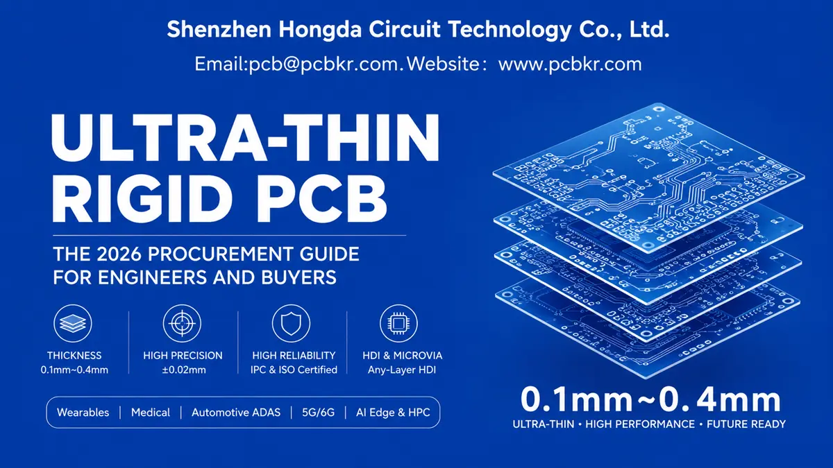
Ultra-Thin Rigid PCB Procurement Guide: How to Source 0.1 mm–0.4 mm Boards Without Yield Surprises
1.What Is an Ultra-Thin Rigid PCB? Definitions That Matter for Buyers
1.1 The 0.4 mm Threshold: Thin PCB vs. Ultra-Thin Rigid PCB Classification

High-tech 3D exploded view demonstrating an ultra-thin rigid PCB stackup architecture, showcasing multi-layer dielectric substrates and fine-line
Ultra Thin Rigid PCB is often poorly defined within procurement RFQ documents, where the generic label “thin PCB” creates widespread ambiguity. In 2026 industry practice, boards between 0.4 mm and 0.6 mm fall under the Thin PCB category—manageable on standard FR4 lines with minor process adjustments. The Ultra‑Thin Rigid PCB segment begins at ≤ 0.4 mm finished thickness, with mainstream production volumes concentrated at 0.3 mm, 0.2 mm, and 0.1 mm, aligning with manufacturer references that classify 0.1 mm‑0.4 mm constructions as ultra‑thin PCB.
This distinction matters because crossing the 0.4 mm boundary fundamentally changes the manufacturing physics. A 1.6 mm standard FR4 board tolerates mechanical drilling misalignment, lamination pressure variance, and moderate copper thickness imbalance. At 0.2 mm, those same tolerances cause panel fracture, Z‑axis expansion failures, and unacceptable bow‑and‑twist during reflow.
1.2 Why Rigid—Not Flex—Matters for Your BOM
Buyers often confuse ultra-thin rigid PCBs with flexible circuits. The critical difference: ultra-thin rigid PCBs retain FR4 or BT glass-reinforced dielectric cores, delivering structural stability for BGA assembly, connector insertion, and thermal cycling—without the polyimide price premium or dynamic-flex reliability concerns. At Shenzhen Hongda Circuit Technology Co., Ltd., our 0.1 mm rigid-flex and pure rigid ultra-thin lines operate in a Class 1000 cleanroom environment, ensuring particulate control during lamination of sub-0.2 mm cores
2. Where Ultra-Thin Rigid PCBs Create Competitive Advantage: Application Mapping
2.1 Consumer Electronics: Wearables, TWS Earbuds, and Ultra-Slim Phone Modules
In wearables, every 0.1 mm of PCB thickness reduction translates to 200+ mAh of additional battery capacity or enhanced ergonomic design freedom
. Our 2026 production data shows that 0.20 mm and 0.30 mm represent roughly 70% of ultra-thin order volume—the sweet spot between miniaturization and SMT yield
2.2 Medical Electronics: Implantable Devices and Endoscope Camera Modules
Implantable devices demand sub-0.3 mm boards with ISO 13485-certified process lanes and biocompatible surface finishes (ENEPIG over standard ENIG). The 0.1 mm–0.2 mm range enables catheter-integrated electronics where flex circuits lack the mechanical rigidity for MEMS sensor mounting.
2.3 Aerospace, Automotive ADAS, and 5G mmWave Modules
Satellite payloads and ADAS camera modules require high-Tg FR-4 (Tg ≥ 170°C) or polyimide (PI) substrates (-269°C to +400°C) to survive thermal shock
. For 5G antenna-in-package (AiP) modules, ultra-thin Rogers/PTFE hybrid stackups reduce insertion loss at 28 GHz.
2.4 AI Edge and High-Performance Computing
AI accelerator cards and 224G PAM4 optical modules push Any-Layer HDI into 0.3 mm–0.4 mm substrates. The shift from 112G to 224G signaling makes through-hole vias obsolete—laser microvias ≤ 75 μm eliminate stub resonance above 56 GHz
3. Material Selection: The Foundation of Ultra-Thin PCB Reliability
3.1 FR-4 High-Tg: The Workhorse for 0.2 mm–0.4 mm Applications
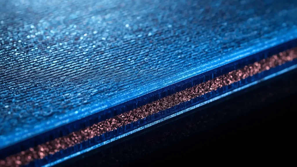
Microscopic cross-section of High-Tg FR-4 substrate, illustrating the glass fiber weave dielectric layer sandwiched with inner copper foil.
For 80% of industrial and consumer applications, high-Tg FR-4 (Tg ≥ 170°C) remains the default. Key parameters buyers must specify:
| Parameter | Standard FR-4 | High-Tg FR-4 (Recommended) |
|---|---|---|
| Tg (DSC) | 130–140°C | ≥ 170°C |
| Dk @ 1 MHz | 4.2–4.8 | 4.2–4.6 |
| CTE (Z-axis) | 50–70 ppm/°C | 45–55 ppm/°C |
| Td (Decomposition) | 300°C | 340°C+ |
At Hongda Circuit, our 2026 stock includes IT-170GRA2 (Tg 175°C) and Megtron 7/8 for low-loss AI server applications
3.2 Polyimide (PI) for Extreme Thermal Environments
When your application exceeds FR-4’s thermal ceiling—automotive under-hood sensors, downhole drilling tools, or aerospace engine monitoring—PI substrates deliver -269°C to +400°C operational range with Dk 3.2–3.5.
3.3 Rogers and Taconic: The RF/Microwave Ultra-Thin Stackup
For 5G mmWave and 6G sub-THz prototypes, specify Rogers RO4350B (Dk 3.48, Df 0.0037) or Taconic TLY-5 in 0.2 mm–0.3 mm builds. These materials require HVLP5 ultra-thin copper foil (≤ 12 μm) and Q-cloth glass weave to minimize signal attenuation at 80 GHz+.
3.4 Copper Foil Thickness: Why 12 μm Inner Layers Change Everything
Standard PCB inner layers use 18 μm or 35 μm copper. In ultra-thin builds, 12 μm (1/3 oz) inner copper is mandatory to preserve dielectric thickness and prevent etch undercut that destroys impedance control. Our mSAP line processes 1.5–3 μm seed layers for 20 μm/20 μm line/space in volume production.
4. Design for Manufacturability: The Buyer’s DFM Checklist
4.1 Stackup Symmetry: Preventing Warpage Before Lamination
The #1 cause of ultra-thin PCB rejection is asymmetric copper distribution. A 0.2 mm board with 35 μm copper on Layer 1 and 12 μm on Layer 2 will bow beyond IPC-6012 Class 3 limits (≤ 0.75%) after the first reflow cycle. Our DFM rule: mirror copper weights across the neutral axis, and never exceed a 2:1 ratio between adjacent layers.
4.2 Fine-Line Geometry: From 3 mil/3 mil to mSAP 20 μm/20 μm

High-density micro-circuitry achieved via mSAP processing, featuring ultra-fine 20 μm trace geometries and laser-drilled microvias
Standard subtractive etching achieves 75 μm (3 mil) line/space reliably. For 0.4 mm pitch BGA escape routing on 0.2 mm boards, specify mSAP (Modified Semi-Additive Process):
- Laminate 1.5–3 μm ultra-thin copper seed
- Image with SCREEN Ledia LDI at ±1.5 μm registration
- Selectively plate to 15–20 μm target height
- Flash-etch seed layer
Result: near-vertical trace sidewalls with ±5% impedance control—critical for MIPI CSI-2 and PCIe Gen5 lanes.
4.3 Microvia Architecture: Stacked vs. Staggered for 0.1 mm–0.3 mm Builds
| Structure | Reliability | Layer Density | Best For |
|---|---|---|---|
| Stacked Microvia | Moderate (stress concentration) | Highest | Consumer wearables, 2–4 layer HDI |
| Staggered Microvia | Highest (distributed stress) | High | Automotive, medical, aerospace |
| Skip-Via | High | Medium | Cost-sensitive IoT modules |
IPC-2226 rule: maximum 2 stacked microvias in standard builds; 3 only with copper-filled VIPPO (Via-in-Pad Plated Over)
. At Hongda Circuit, our 3D CT X-ray inspection validates void rates < 3% before surface finishing
4.4 Impedance Control in Ultra-Thin Dielectrics
A 0.2 mm 4-layer board with 0.09 mm prepreg between L1-L2 requires 50 Ω single-ended traces at 75 μm width—unachievable with standard etching. Our AI-driven etch compensation system (validated on 600+ panels in Q2 2026) improved impedance Cpk from 1.18 to 1.61 by adjusting spray pressure and conveyor speed in real time.
4.5 Panelization and Tooling Holes: The Hidden Yield Killer
Ultra-thin panels warp during conveyor transport. Specify 0.5 mm minimum tooling holes on 3-point registration, and add 5 mm carrier rails on all edges for automated handling. Remove rails after SMT via precision routing—never V-score sub-0.3 mm boards, as the stress fractures inner layer microvias.
5. Manufacturing Process: Where Ultra-Thin PCBs Succeed or Fail
5.1 Material Handling and Layup: The First 60 Seconds Decide Yield
Standard PCB layup uses vacuum-assisted pin lamination. At 0.1 mm–0.2 mm core thickness, mechanical pinning tears the glass weave. Our solution: electrostatic layup tables with ionized air knives and optical edge alignment (±25 μm) before pressing. Core materials are pre-conditioned at 23°C / 50% RH for 24 hours to stabilize dimensional expansion.
5.2 Sequential Lamination: Thin-Core vs. Coreless Buildups
For 6+ layer ultra-thin boards, we deploy thin-core lamination (0.025 mm cores) and low-pressure lamination (≤ 200 psi) to prevent resin starvation and inner-layer shift
. Our LAUFFER lamination system maintains ±0.02 mm dielectric thickness tolerance across 610 × 544 mm panels.
5.3 Laser Drilling: UV vs. CO₂ for Microvia Quality
| Laser Type | Wavelength | Best For | Via Size | Position Accuracy |
|---|---|---|---|---|
| CO₂ | 10.6 μm | Blind vias in build-up layers | 100–150 μm | ±15 μm |
| UV (355 nm) | 355 nm | Ultra-HDI, copper direct ablation | 50–75 μm | ±10 μm |
| Picosecond | 532 nm | High-Tg materials, minimal HAZ | < 50 μm | ±8 μm |
Our Mitsubishi UV/CO₂ dual-head systems achieve 75 μm microvias with ±10 μm positional accuracy on 0.1 mm builds
5.4 Electroplating: Uniformity in High-Aspect-Ratio Microvias
Ultra-thin boards with 0.075 mm microvias in 0.09 mm dielectric create 1.2:1 aspect ratios—approaching the plating chemistry limit. Our 2026-generation 3-in-1 horizontal plating line maintains < 5% uniformity error and void-free fill, validated by microsection per IPC-TM-650
5.5 Solder Mask and Legend Printing: Fixture-Dependent Precision
Standard screen printing collapses 0.2 mm panels. We use vacuum-assisted pinless fixtures with 30 μm emulsion screens for solder mask, followed by LDI direct imaging for legends—eliminating phototool stretch that shifts 0.1 mm pitch component markings.
5.6 Routing and Singulation: Why Laser Routing Beats Milling for 0.1 mm Boards
Mechanical routing at 30,000 RPM generates heat and vibration that delaminates 0.1 mm edges. For sub-0.2 mm boards, specify UV laser routing with 20 μm kerf width and nitrogen assist—zero mechanical stress, clean glass-fiber edges.
6. SMT Assembly and Reliability: What Buyers Must Specify Upstream
6.1 Reflow Profile Control: The 170°C Tg Ceiling
Standard lead-free reflow peaks at 245–250°C. For high-Tg ultra-thin boards, specify ramp rates ≤ 1.5°C/second above 150°C to prevent Z-axis expansion cracking. Our DFM team provides reflow simulation data (Siemens Simcenter) before stencil design.
6.2 Component Mass Limits: The 0201/01005 Transition
On 0.2 mm substrates, components > 50 mg per pad create pad-lift risk during thermal cycling. Specify 0201 or 01005 passives, CSP/BGA packages under 8 × 8 mm, and avoid through-hole connectors unless mechanically reinforced with stiffeners.
6.3 Reliability Testing Protocols for Ultra-Thin Rigid PCBs
| Test | Condition | Acceptance Criteria |
|---|---|---|
| Thermal Cycling | -55°C to +125°C, 1000 cycles | No via cracking, ΔR < 10% |
| TCT (IST) | 25°C to 150°C, 6 min cycle | 300 cycles, no open/short |
| Mechanical Bend | 1 mm radius, 90° deflection | No trace fracture (IPC-6012C) |
| HAST | 130°C / 85% RH / 33.3 psi, 96 hr | No delamination, no CAF |
Our in-house IST (Interconnect Stress Test) lab validates microvia reliability before volume release.
7. Cost, Lead Time, and Yield: The Procurement Reality
7.1 Material Cost Drivers: Why High-Tg FR-4 Costs 40% More Than Standard
Ultra-thin high-Tg FR-4 laminates carry a 25–40% premium over standard 1.6 mm material due to reduced yield at the prepreg manufacturer and specialized thin-core handling. PI substrates add 2–3× cost but eliminate the need for thermal interface materials in high-temperature applications.
7.2 Process Complexity Multipliers
| Feature | Cost Impact | Why |
|---|---|---|
| mSAP vs. subtractive | +50–150% | LDI imaging, selective plating, cleanroom |
| Any-Layer HDI (Type VI) | +80–200% | 6+ sequential lamination cycles |
| 0.1 mm vs. 0.3 mm | +30–50% | Special handling, lower panel utilization |
| Impedance control ±5% | +15–25% | 100% TDR testing, coupon validation |
7.3 Yield Realities: Planning for 85–92% First-Pass Yield
Ultra-thin PCB first-pass yield typically runs 8–15% below standard boards due to handling damage, microvia voids, and warpage. At Hongda Circuit, our AI-assisted AOI + 3D X-ray inspection protocol improves yield by 15% versus traditional methods by catching line scratches and copper residues invisible to human operators
7.4 Lead Time Expectations: From 24-Hour Quote to 7-Day Prototype
| Volume | Standard Lead Time | Expedited |
|---|---|---|
| Prototype (5–20 panels) | 7–10 days | 3–5 days (+30%) |
| NPI (50–200 panels) | 12–15 days | 7–10 days (+40%) |
| Volume (500+ panels) | 15–20 days | 10–12 days (dedicated line) |
Our AI-driven ERP system maintains > 95% on-time delivery with real-time DHL/FedEx tracking from Shenzhen to global hubs.
8. Supplier Qualification: The 7-Point RFQ Checklist for Ultra-Thin Rigid PCB Vendors
8.1 Minimum Thickness Verification: Ask for Microsection Photos
Any supplier claiming 0.1 mm capability should provide dated microsection images showing copper thickness, dielectric integrity, and microvia fill quality. Red flag: suppliers who quote 0.1 mm but only show 0.3 mm samples.
8.2 HDI and Microvia Capability Matrix
Verify:
- Laser drilling minimum: ≤ 75 μm for standard, ≤ 50 μm for advanced
- Layer-to-layer registration: ±10 μm or better
- Sequential lamination cycles: ≥ 4 for Any-Layer HDI
- mSAP qualification: 20 μm/20 μm in production, 8 μm/8 μm for SLP
8.3 Material Certifications and Traceability
Mandatory: ISO 9001:2015, IPC-6012 Class 3, UL 94V-0, RoHS 3/REACH. For automotive: IATF 16949. For medical: ISO 13485. For aerospace: AS9100D.
8.4 DFM Collaboration: Not a Sales Pitch, a Technical Necessity
A qualified ultra-thin PCB supplier provides pre-tooling stackup review, impedance simulation, and reflow profile recommendations—not just a quote. Our engineering team delivers 1-hour engineering evaluation and 24/7 technical support during NPI ramp.
8.5 Equipment Audit: What to Look for on a Factory Tour
| Equipment | Function | Minimum Specification |
|---|---|---|
| LDI (Laser Direct Imaging) | Trace patterning | ±1.5 μm registration, SCREEN or Orbotech |
| UV Laser Driller | Microvia formation | 355 nm, ±10 μm accuracy |
| Vacuum Lamination Press | Layer bonding | ≤ 200 psi, ±2°C uniformity |
| 3D AOI + AI | Defect detection | 1 μm pixel resolution, deep-learning classification |
| TDR/VNA | Impedance validation | 40 GHz bandwidth, 4-port S-parameter |
8.6 Quality Documentation: What Ships with Every Lot
Demand: microsection report, impedance coupon data, IST microvia reliability report, XRF surface finish thickness, and CofC (Certificate of Conformance). At Hongda Circuit, every ultra-thin lot includes full traceability data from raw material lot numbers to final electrical test.
8.7 Geographic Risk: Why Shenzhen-Based Manufacturing Matters
Approximately 70% of advanced substrate production capacity is concentrated in Asia
. Shenzhen’s ecosystem provides same-day material sourcing from Kingboard, Shengyi, and Rogers distributors—reducing lead times by 40% versus Western alternatives
FAQ: What Procurement Engineers Ask Before Placing an Ultra-Thin Rigid PCB Order
How Do I Verify a Supplier’s Real 0.1 mm Rigid PCB Capability vs. Marketing Claims?
Request three documents: (1) a microsection photograph of a 0.1 mm production board showing dielectric thickness and copper weight, (2) IST test data for microvia reliability on thin cores, and (3) IPC-6012 Class 3 certification scope specifically covering ≤ 0.2 mm boards. A vendor with genuine capability will provide these within 24 hours. At Hongda Circuit, we maintain live DFM dashboards where buyers validate stackup feasibility before committing to tooling.
What Is the True Cost Difference Between 0.2 mm and 0.4 mm Ultra-Thin FR4 PCBs?
Expect a 20–35% cost premium for 0.2 mm versus 0.4 mm at equivalent layer counts, driven by: (a) lower panel utilization (specialized handling frames reduce usable area by 15%), (b) higher scrap rates during routing, and (c) premium thin-core material pricing. However, at volume (500+ panels/month), the delta compresses to 10–15% as yield optimization and dedicated line allocation take effect. Request a volume-price curve in your RFQ to model break-even points.
Can Standard SMT Lines Assemble 0.1 mm–0.2 mm Rigid PCBs, or Do I Need Specialized Equipment?
Standard SMT lines can handle 0.3 mm+ boards with minor conveyor adjustments. For 0.1 mm–0.2 mm substrates, you must specify: (1) vacuum-supported reflow fixtures to prevent panel sagging, (2) reduced reflow peak temperature (235–240°C vs. 245°C) to minimize warpage, and (3) component mass limits (≤ 50 mg per 0201 pad). Hongda Circuit provides assembly-ready DFM packages including recommended stencil aperture ratios and thermal profile simulations for each stackup.
How Do I Prevent Warpage and Bow-Twist in Ultra-Thin Multilayer PCBs During Reflow?
Warpage is 90% preventable at the design stage. Specify: (1) symmetric copper distribution (mirror layer weights across the neutral axis), (2) balanced prepreg resin content (never mix 7628 and 1067 glass styles asymmetrically), (3) 0.5 mm minimum board edge keep-out for components to reduce localized stress, and (4) baking at 125°C for 4 hours before SMT to relieve moisture-induced expansion. Our pre-production warpage simulation (ANSYS Mechanical) predicts bow/twist values before lamination begins.
What Should My Ultra-Thin Rigid PCB RFQ Include to Get an Accurate Quote in 24 Hours?
Include these 8 fields for zero-back-and-forth quoting:
1. Finished thickness (e.g., 0.2 mm ± 0.02 mm)
2. Layer count and stackup (e.g., 4-layer, 1+2+1 HDI)
3. Base material (e.g., FR-4 IT-170, Tg 170°C)
4. Copper weight (outer/inner, e.g., 1/2 oz outer, 1/3 oz inner)
5. Minimum trace/space (e.g., 3 mil/3 mil or 75 μm/75 μm)
6. Microvia spec (e.g., 0.1 mm laser-drilled blind via, copper-filled)
7. Surface finish (e.g., ENIG 2–4 μin Au, or ENEPIG for wire bonding)
8. Impedance requirements (e.g., 50 Ω ± 5% single-ended, 100 Ω ± 5% differential)
Omitting any of these triggers engineering questions that delay quoting by 2–3 days. Submit your complete spec to sales@pcbkr.com for same-day technical evaluation.
Making the Ultra-Thin Rigid PCB Decision with Confidence
Sourcing ultra-thin rigid PCBs at 0.1 mm–0.4 mm is no longer a niche engineering exercise—it is a mainstream procurement competency for wearables, medical devices, 5G modules, and AI edge hardware. The difference between a successful NPI and a 3-month delay lies in supplier qualification rigor: verifying real mSAP capability, demanding microsection evidence, and insisting on DFM collaboration before tooling release.
At Shenzhen Hongda Circuit Technology Co., Ltd. (PCBKR), our 2026 manufacturing platform combines mSAP fine-line processing, 75 μm UV laser microvias, AI-driven impedance control, and Class 1000 cleanroom lamination to deliver ultra-thin rigid PCBs with first-pass yields that meet automotive and medical reliability standards. Whether your next project requires a 0.1 mm sensor card or a 0.3 mm 12-layer Any-Layer HDI for 5G mmWave, our engineering team provides the technical depth and manufacturing transparency that procurement teams need to de-risk their supply chain.
Ready to validate your ultra-thin stackup? Send your Gerber and stackup requirements to sales@pcbkr.com for a 1-hour DFM review and 24-hour prototype quotation.
About Author
David Chen https://www.linkedin.com/in/pcbcoming
David Chen boasts an extensive professional background in PCBA manufacturing, PCBA testing, and PCBA optimization, with specialized expertise in high-precision PCBA fault analysis and rigorous PCBA reliability testing. The author has worked with high-layer-count server PCB fabrication, ultra-low-loss backplane stackups, and thermo-mechanical reliability optimization for AI infrastructure projects involving 112G and 224G PAM4 architectures. Skilled in complex circuit design and cutting-edge advanced PCB manufacturing processes, he delivers solutions that elevate product durability and performance across industrial applications. His technical articles focusing on PCBA manufacturing workflows and testing methodologies are widely cited by industry peers, research institutions, and technical platforms, solidifying his reputation as a recognized technical authority in the global circuit board manufacturing sector.