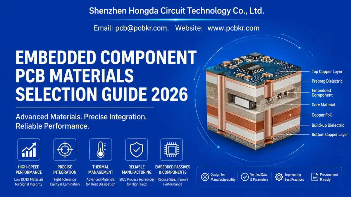
Embedded Component PCB Materials: 2026 Selection Guide for High-Density PCB Manufacturing
Embedded component PCB materials must be selected as a complete electrical, mechanical and manufacturing system—not as a laminate brand alone. For 2026 designs, the decision should link dielectric Dk/Df, copper roughness, resin flow, cavity geometry, CTE, thermal performance, component compatibility, and measurable impedance or reliability targets to the actual stack-up.
This revised guide expands the supplied article into a procurement- and engineering-oriented 2026 version. The original source correctly identifies the interaction among component, cavity, dielectric, copper and build-up structure as the central material-selection issue.
What materials are used in an embedded component PCB?
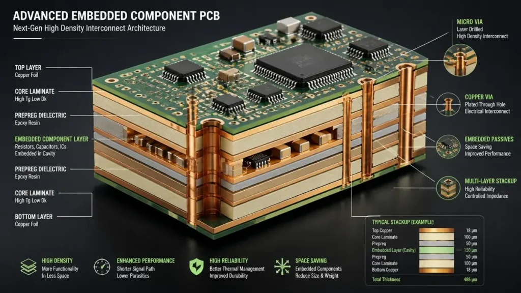
Embedded Component PCB Materials – Advanced 3D Stackup Architecture
Direct answer: A production embedded PCB normally combines core laminates, prepreg or build-up dielectric, copper foil, resin systems, embedded passive or active devices, and—when required—thermal or conductive structures.
The supplied source identifies core materials, prepreg, build-up dielectrics, copper foil, resin systems, embedded-component materials, conductive structures and thermal-management materials as the main material groups.
The engineering mistake is to treat these materials independently. A 0.10 mm cavity, for example, is not simply a mechanical hole: its dimensions affect resin displacement, local dielectric thickness, copper registration, via landing geometry and the stress transferred into the embedded component during lamination.
For a buyer, the RFQ should therefore specify the functional requirement first and the material family second. A supplier should be able to show the proposed stack‑up, material construction, component envelope, lamination strategy and verification method before material substitution is approved. For end‑to‑end technology overview, design challenges and supplier procurement evaluation workflows, please refer to our Embedded Component PCB: Technology, Manufacturing & Procurement Guide
Why is dielectric selection critical for embedded component PCB performance?
Direct answer: Dielectric selection controls electrical spacing, impedance, capacitance, propagation behavior, thermal expansion and lamination response; for high-speed designs, Dk and Df must be evaluated together with copper geometry and frequency.
The source article identifies layer thickness, impedance, capacitance, signal propagation, thermal expansion, lamination behavior and mechanical stability as direct consequences of dielectric choice.
For 2026 high-speed designs, do not place a single Dk value on the purchase order and assume signal integrity is controlled. The effective impedance depends on dielectric thickness, trace width, copper thickness, copper roughness, glass-weave position and the actual cured resin content.
A useful procurement specification is to define the target impedance, nominal dielectric thickness and tolerance, Dk/Df measurement frequency or method, copper roughness requirement, and the stack-up revision against which the supplier must manufacture. IPC maintains test methods for Dk/Df, TDR impedance and high-frequency signal-loss characterization, including IPC-TM-650 methods 2.5.5.15, 2.5.5.7A and 2.5.5.14.
How should Dk and Df be specified for high-speed embedded PCBs in 2026?
Direct answer: Specify Dk and Df at the frequency and test method relevant to the channel, then validate the finished stack-up; do not select a material from a low-frequency Dk number alone.
For a 56 GHz-class channel, a material comparison can use a project-specific target such as Df ≤0.0025 at the relevant test frequency, but the actual allowable value must come from the channel-loss budget and qualified laminate data rather than a universal rule.
The more important engineering control is consistency: material lot, resin content, cured dielectric thickness, copper profile and trace geometry must remain within the stack-up model. A nominal Dk mismatch of only a few hundredths can become significant when the dielectric is thin and impedance tolerance is tight.
For embedded structures, the material surrounding the component is also mechanically active. Resin shrinkage and CTE mismatch can transfer stress into the component and surrounding dielectric during lamination and thermal cycling. Published research on embedded flip-chip structures identifies CTE mismatch, solder fatigue and resin fracture as important thermo-mechanical reliability considerations.
How does copper foil selection affect embedded PCB signal integrity and manufacturability?
Direct answer: Copper thickness and surface profile must be selected together with line width, frequency and plating build; lower-profile copper becomes increasingly important as channel frequency rises.
The supplied article correctly identifies copper thickness, foil type, surface profile, roughness and plating thickness as the key copper parameters.
At high frequency, current crowds near the conductor surface, so roughness can increase effective conductor loss and disturb the modeled impedance. For a 56 GHz-class application, an engineering team may evaluate VLP/ULP/HVLP copper with an Rz target around 0.3–1.0 µm depending on the laminate, etch process and loss budget. This is a design target, not a universal acceptance limit.
Manufacturing pain point: specifying ultra-smooth copper without checking adhesion and etchability can create a different failure mode. The foil must survive oxide or alternative surface treatment, lamination, fine-line etching and plating without unacceptable peel strength, undercut or trace-width drift.
For procurement, request the copper foil grade, nominal thickness, roughness metric (Ra/Rz), measurement method, plating allowance and finished conductor thickness—not simply ‘1 oz copper’.
What are the biggest manufacturing pain points when selecting materials for embedded PCB cavities?
The dominant problems are resin flow, cavity dimensional tolerance, component movement, void formation, local dielectric-thickness variation, lamination stress, warpage and registration loss.
The supplied source specifically flags cavity filling, void formation, local thickness, component stress, bonding and warpage as material-dependent lamination issues.
Pain point 1 — Resin starvation: too little resin around a cavity can leave incomplete bonding or voids; too much flow can intrude into a controlled cavity and change component clearance.
Pain point 2 — Component movement: a component can shift during pressing if the cavity, adhesive system and restraining structure are not designed as a process window rather than a nominal dimension.
Pain point 3 — Local thickness: copper topography and component height can consume the available resin-flow volume. A stack-up that looks correct in CAD may produce a different cured dielectric thickness after pressing.
Pain point 4 — Warpage: asymmetric copper distribution, dissimilar CTE and non-uniform resin content can create panel curvature that later affects drilling, routing, SMT and final assembly.
Pain point 5 — Void detection: visual inspection cannot prove internal bonding quality. Cross-sectioning, X-ray or other qualified non-destructive methods should be selected according to the component and reliability requirement.
A practical supplier review should therefore ask for the lamination recipe window, cavity tolerance, component placement tolerance, void acceptance criterion, cross-section plan and evidence of first-article stack-up verification.
How should materials be selected for embedded resistors and capacitors?
Direct answer: The material must meet the required electrical value while remaining compatible with the PCB fabrication process, lamination cycle, laser/drill operations and reliability test plan.
The supplied article makes this key distinction explicitly: embedded passive material selection must satisfy both the electrical target and PCB manufacturing compatibility.
Embedded resistor technologies can use dedicated resistive films or other internal structures. The buyer should specify nominal resistance, tolerance, power-density requirement, trimming strategy if applicable, temperature coefficient, dielectric environment and long-term stability.
For embedded capacitive structures, the engineering variables include dielectric thickness, dielectric constant, electrode area, copper thickness and local geometry. The capacitance target should be verified on representative test structures because cured resin content and dimensional tolerance change the effective result.
Do not accept a component material solely because its datasheet electrical value looks attractive. The decisive question is whether the material can be repeatedly integrated into the intended multilayer construction.
What 2026 PCB manufacturing technologies should be considered with embedded components?
Direct answer: The most relevant technology stack combines advanced HDI/microvia processing, high-accuracy laser drilling, fine-line imaging, controlled lamination, low-profile copper, high-frequency material characterization, automated optical inspection and electrical verification.
IPC-6012F explicitly covers rigid multilayer boards with buried/blind vias and microvias as well as active/passive embedded circuitry; IPC also identifies IPC-7092 as the design and assembly implementation standard for embedded circuitry.
2026 manufacturing practice increasingly treats the embedded component zone as a controlled three-dimensional process window. Laser drilling can be used for microvias and controlled interconnect formation, while high-resolution imaging and automated inspection reduce registration and fine-line risks.
For high-speed embedded boards, material characterization should include appropriate Dk/Df testing and finished-board signal verification. IPC’s TM-650 library includes methods for high-frequency signal loss, TDR impedance and Dk/Df measurement.
For advanced designs, mSAP/SAP-style fine-line processing may be considered when the routing density requires it. The technology should be selected from the actual line/space, copper thickness, plating and yield target—not because the process name sounds more advanced.
Which material parameters should a PCB buyer put into an embedded PCB RFQ?
Direct answer: The RFQ should contain measurable electrical, mechanical, thermal, dimensional and reliability parameters, plus the evidence required for first-article approval.
Recommended parameter matrix:
• Laminate family and manufacturer-approved equivalent: define whether substitutions require written approval.
• Cured dielectric thickness: nominal value plus tolerance, especially around cavity and impedance layers.
• Dk/Df: specify test method and frequency or frequency band.
• Copper: finished thickness, foil type, roughness metric and target value.
• Trace geometry: minimum line/space, finished line-width tolerance and plating allowance.
• Cavity: length, width, depth, corner radius and dimensional tolerance.
• Component placement: X/Y tolerance, rotation tolerance and allowable clearance to copper.
• Lamination: resin-flow strategy, maximum pressure/temperature exposure and void-control requirement.
• Thermal: Tg, Z-axis CTE and any thermal-conductivity target relevant to the application.
• Reliability: thermal cycling, solder/reflow exposure, insulation resistance, CAF or other application-specific tests.
• Inspection: cross-section frequency, X-ray/AOI requirements, electrical test and impedance verification.
This approach is consistent with the supplied source’s recommendation to specify laminate family, dielectric thickness, copper thickness, surface finish, thermal requirements, impedance, high-frequency requirements, component material and reliability requirements.
Which embedded PCB manufacturing scenarios require the most careful material engineering?
Direct answer: High-speed computing, RF modules, miniaturized wearables, medical electronics, automotive control units and power-dense products are especially sensitive because electrical, mechanical and thermal requirements interact.
Scenario 1 — AI/networking hardware: embedded passives can shorten local interconnects and free routing area, but low-loss dielectric and low-profile copper become important as channel frequency rises.
Scenario 2 — Compact RF module: the material system must control Dk/Df, conductor roughness and dimensional stability while avoiding cavity or component placement errors that shift the RF geometry.
Scenario 3 — Wearable or miniature electronics: the value proposition is often area reduction. The engineering risk is that a small cavity leaves very little tolerance for component movement, resin squeeze-out or warpage.
Scenario 4 — Thermal-dense electronics: copper structures or thermal materials can be integrated with embedded devices, but thermal expansion mismatch must be checked against the surrounding laminate and component package.
Scenario 5 — High-reliability products: the supplier must demonstrate that the embedded construction survives the same environmental and thermal exposures as the rest of the board.
How can a buyer verify that an embedded PCB supplier really controls the material process?
Direct answer: Ask for objective manufacturing evidence tied to the exact stack-up: incoming material certificates, dimensional inspection, cross-sections, impedance results, void/lamination evidence and reliability data.
A credible qualification package should connect the material lot to the manufactured panel. At minimum, the supplier should be able to identify the laminate construction, copper specification, dielectric build and process revision used for the first article.
For high-speed boards, ask for TDR or equivalent impedance results and, when required by the channel design, insertion-loss characterization. For embedded cavities, ask for cross-sections through the cavity edge, component interface and critical via structures.
IPC-6012F expanded requirements in areas including printed-board cavities, hole registration, internal plated layers, dielectric spacing and microvia reliability, making it a useful framework for qualification discussions.
The engineering rule is simple: a supplier’s capability statement is not process evidence. A buyer should qualify the exact construction, not a generic factory capability list.
What is the best material-selection strategy for Shenzhen Hongda Circuit Technology Co., Ltd. projects?
Direct answer: Start with the electrical and mechanical requirements, build the stack-up around the embedded component geometry, then freeze materials only after manufacturing compatibility and verification methods are agreed.
Our recommended workflow is: 1) define component type and envelope; 2) define signal, power and thermal requirements; 3) create the preliminary stack-up; 4) select dielectric and copper families; 5) model cavity and resin-flow conditions; 6) review drilling/microvia strategy; 7) manufacture a first article; 8) cross-section and electrically verify the construction; 9) close the process window before volume production.
This sequence prevents a common procurement failure: selecting the cheapest laminate first and discovering later that the dielectric thickness, resin flow, copper roughness or CTE is incompatible with the board architecture.
For supplier RFQs, Shenzhen Hongda Circuit Technology Co., Ltd. recommends treating the stack-up, embedded-component specification and verification plan as one controlled engineering package.
2026 Embedded Component PCB Material Parameter Checklist
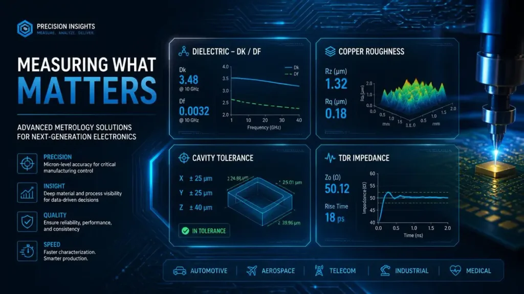
Embedded PCB Material Parameter Checklist & Testing Metrics
| Parameter | Engineering target / example | Why it matters | Verification |
| Dielectric thickness | Project nominal ± agreed tolerance | Impedance, cavity clearance, capacitance | Microsection / thickness measurement |
| Dk / Df | Frequency-specific; use qualified laminate data | Loss, phase delay, impedance | IPC-TM-650 method appropriate to frequency |
| Copper roughness | VLP/ULP/HVLP selected to loss budget | High-frequency conductor loss | Profilometry / supplier CoA |
| Finished copper | Defined by layer and current capacity | Resistance, etchability, reliability | Microsection / thickness test |
| Cavity size | CAD dimension with process tolerance | Component fit and resin flow | Optical / dimensional inspection |
| Component placement | Defined X/Y/rotation tolerance | Via landing and electrical geometry | AOI / X-ray / cross-section |
| Tg / CTE | Application-specific, high-reliability where required | Thermal cycling and warpage | Material certificate / TMA / DSC |
| Void criterion | Defined by component and reliability class | Bonding and reliability | X-ray / microsection |
| Impedance | Typically 50 Ω single-ended or 90/100 Ω differential as designed | Signal integrity | TDR |
| Reliability | Application-specific test plan | Long-term field performance | Thermal cycling / IST / CAF etc. |
Procurement FAQs: What Buyers Search Before Choosing an Embedded PCB Supplier
Can a PCB manufacturer supply the laminate, embedded component integration and HDI process from one controlled stack-up?
A strong supplier should be able to review the complete stack-up rather than quote the laminate separately. Ask for the component envelope, cavity design, dielectric construction, microvia strategy and verification plan as one engineering package.
What material data should I request before approving an embedded component PCB supplier?
Request laminate construction, cured dielectric thickness, Dk/Df data with test method, copper thickness and roughness, Tg/CTE, component compatibility, cavity tolerance and the planned inspection evidence. Avoid approving a supplier from a material brand name alone.
Can embedded component PCBs use low-loss materials for high-speed signals?
Yes. Low-loss laminates and low-profile copper can be combined with embedded structures, but the stack-up must be modeled and then verified on the finished board. Dk/Df, copper roughness, dielectric thickness and impedance should be treated as a coupled system.
What is the biggest manufacturing risk when buying embedded component PCBs?
The highest risk is usually the interaction between cavity geometry, component placement and lamination. Resin flow, voids, component movement, local dielectric thickness and warpage can create defects that are invisible from the Gerber files alone
How should I compare two embedded PCB suppliers on price and quality?
Compare the same controlled construction: material grade, dielectric build, copper specification, cavity tolerance, component placement tolerance, via technology, inspection plan, first-article evidence, reliability testing and lead time. A lower unit price is not comparable if the supplier has relaxed any of these parameters.
Technical Reference Basis
User-supplied source: Embedded Component PCB Materials: Selection Guide.
IPC-6012F: Qualification and Performance Specification for Rigid Printed Boards; includes multilayer boards with microvias and active/passive embedded circuitry.
IPC-7092: Design and Assembly Process Implementation for Embedded Circuitry.
IPC-TM-650: relevant test methods include Dk/Df characterization, TDR impedance, high-frequency signal loss and embedded passive material testing.
About Author
David Chen https://www.linkedin.com/in/pcbcoming
David Chen boasts an extensive professional background in PCBA manufacturing, PCBA testing, and PCBA optimization, with specialized expertise in high-precision PCBA fault analysis and rigorous PCBA reliability testing. The author has worked with high-layer-count server PCB fabrication, ultra-low-loss backplane stackups, and thermo-mechanical reliability optimization for AI infrastructure projects involving 112G and 224G PAM4 architectures. Skilled in complex circuit design and cutting-edge advanced PCB manufacturing processes, he delivers solutions that elevate product durability and performance across industrial applications. His technical articles focusing on PCBA manufacturing workflows and testing methodologies are widely cited by industry peers, research institutions, and technical platforms, solidifying his reputation as a recognized technical authority in the global circuit board manufacturing sector.