Embedded Component PCB IPC Standards: A Manufacturing and Procurement Guide
Embedded Component PCB IPC Standards, primarily guided by IPC-7092A for design and process implementation, require pairing with performance specifications such as IPC-6017A and IPC-6012F based on the board’s embedded structure, HDI construction, materials, assembly process, product class, and reliability demands. Rather than simply claiming “IPC compliant,” a reliable supplier converts these standards into measurable fabrication, inspection, and traceability controls.
Why Is IPC‑7092A Important for Embedded Component PCB Manufacturing?
IPC‑7092A is important because embedded PCB manufacturing combines component integration, multilayer lamination, electrical interconnection, inspection, assembly and reliability into one manufacturing flow.
The original document correctly identifies IPC‑7092 as the dedicated reference for embedded circuitry design and assembly implementation.
IPC’s current design‑standard information lists IPC‑7092 as “Design and Assembly Process Implementation for Embedded Circuitry.” The current revision is IPC‑7092A, released in 2022.
For a PCB manufacturer, this distinction matters.
An embedded component PCB is not simply:
PCB fabrication + component placement.
It is a controlled integration of:
- PCB material selection
- Inner‑layer circuit formation
- Embedded resistor/capacitor or active‑device integration
- Component cavity or placement structure
- Lamination
- Laser drilling
- Microvia formation
- Copper plating
- Via filling
- Outer‑layer imaging
- Surface finishing
- SMT/through‑hole assembly
- Electrical testing
- Cross‑section analysis
- Reliability verification
IPC‑7092A specifically addresses the design, material and assembly challenges associated with embedded circuitry and the transition to subsequent surface‑mount or through‑hole assembly.
Engineering experience: the real problem is process interaction
In production, the difficult part is rarely one individual operation.
The difficult part is what happens between operations.
For example, an embedded component may pass an incoming inspection but fail after lamination because:
- component thickness was not matched to the dielectric stack‑up;
- resin flow was not adequately controlled;
- copper balance was poor;
- the component created a local pressure discontinuity;
- the embedded component shifted during lamination;
- subsequent laser drilling referenced the wrong effective datum.
This is why an embedded PCB should be engineered as a single manufacturing system, not as independent PCB and component processes.
Which IPC Standards Apply to an Embedded Component PCB?
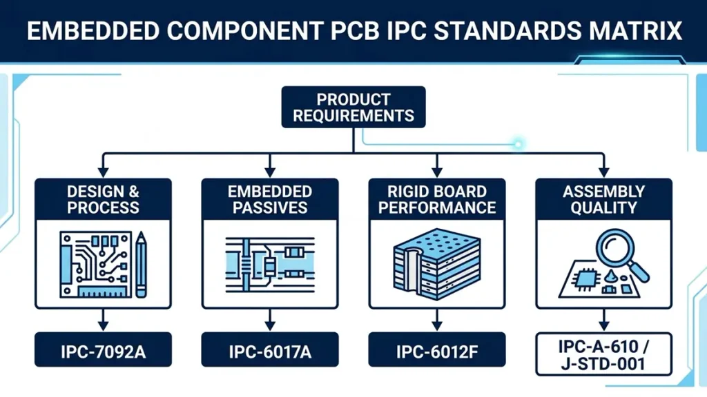
Embedded Component PCB IPC Standards Matrix – Hongda Circuit
There is no single IPC standard that automatically covers every embedded PCB requirement; the correct compliance matrix depends on PCB construction, embedded technology, HDI architecture, materials, assembly and end‑use reliability.
The source article correctly emphasizes that embedded PCBs can simultaneously involve multilayer fabrication, HDI, microvias, embedded passive components, active devices and advanced assembly.
A practical 2026 standards structure is:
| Engineering area | Relevant IPC reference |
|---|---|
| Embedded circuitry design/process | IPC‑7092A |
| Embedded passive‑device performance | IPC‑6017A |
| Rigid PCB performance | IPC‑6012F |
| Generic PCB design | IPC‑2221C |
| HDI design | IPC‑2226 |
| Base materials | IPC‑4101 series |
| High‑speed/controlled impedance | Applicable IPC high‑speed design guidance |
| Assembly soldering | IPC J‑STD‑001 |
| Assembly acceptability | IPC‑A‑610 |
| BGA design | IPC‑7095 |
| Manufacturing data transfer | IPC‑2581 |
| Traceability | IPC‑1782 |
IPC’s standards resources confirm that IPC‑2221C is the current generic board‑design revision listed by IPC, while IPC‑6012F is the current rigid‑board performance specification.
Importantly, IPC‑6012F explicitly includes multilayer boards with blind/buried vias/microvias and active/passive embedded circuitry.
Therefore, a purchasing specification that says only:
“PCB shall meet IPC standards”
is technically incomplete.
Does IPC‑7092A Replace Other PCB Standards?
No. IPC‑7092A should be treated as part of a broader standards system rather than as a replacement for PCB performance, HDI, material, assembly or reliability specifications.
The uploaded article makes this point directly: applicable requirements depend on construction, component type, HDI structure, assembly process, product class, reliability requirements and customer specifications.
A better engineering approach is to build a hierarchy:
Product requirements → PCB architecture → Embedded technology → Applicable IPC standards → Manufacturing controls → Inspection → Reliability qualification
For example:
Example: Embedded resistor + HDI + BGA
A board may simultaneously require:
- IPC‑7092A for embedded‑circuitry implementation
- IPC‑6017A for embedded passive circuitry
- IPC‑6012F for rigid‑board performance
- IPC‑2226 for HDI design considerations
- IPC‑7095 for BGA‑related design
- IPC‑A‑600 for bare‑board acceptability where applicable
- J‑STD‑001/A‑610 for the assembly stage
This is exactly why the original article recommends an application‑specific standards matrix rather than treating IPC‑7092 as the only applicable document. For end‑to‑end technology overview, design challenges and supplier evaluation workflows for embedded‑component projects, please refer to our Embedded Component PCB: Technology, Manufacturing & Procurement Guide.
What Manufacturing Technologies Should Be Added to an Embedded Component PCB in 2026?
The most useful 2026 manufacturing upgrades are not a single “new machine,” but the integration of high‑density imaging, laser microvia processing, advanced via filling, controlled lamination, automated optical inspection, X‑ray inspection, microsection analysis and digital process traceability.
1. Laser Direct Imaging — LDI
LDI is increasingly valuable for fine‑line and HDI structures because artwork registration can be digitally controlled without relying on conventional phototool registration.
For advanced embedded HDI boards, engineering targets may include:
- Fine‑line geometry down to approximately 50/50 µm for selected structures
- Tighter layer‑to‑layer registration than conventional coarse‑pitch designs
- Laser‑formed microvias
- Sequential build‑up layers
However, these are manufacturing capability targets, not universal IPC acceptance limits. The actual minimum should be established from the supplier’s equipment, material system, copper thickness and yield history.
2. Laser Microvia Drilling
Modern embedded HDI boards commonly use laser‑drilled microvias to reduce routing area and connect build‑up layers.
Typical engineering ranges may include:
- Microvia diameter: approximately 50–100 µm
- Target aspect ratio: often controlled around 0.8:1 to 1:1
- Sequential build‑up: 1+N+1, 2+N+2 or more complex constructions
- Laser depth controlled by dielectric thickness
The actual specification must be established from the stack‑up and reliability requirement.
3. Copper‑Filled Microvias
Copper‑filled microvias become particularly important where:
- stacked microvias are required;
- via‑in‑pad is used;
- BGA pitch is tight;
- embedded components reduce available routing channels.
IPC‑6012F specifically expanded attention to microvia reliability, copper‑wrap plating, internal plated layers and related structural considerations.
This is an important manufacturing issue because a via can look acceptable externally while having an internal defect.
Therefore, our engineering inspection should not stop at AOI.
A qualification structure may include:
AOI → electrical test → microsection → dimensional measurement → reliability testing
IPC also provides coupon concepts for evaluating stacked and staggered blind/buried‑via structures and structural integrity.
What Are the Most Difficult Manufacturing Problems in Embedded Component PCBs?
The hardest problems are component displacement, resin‑flow imbalance, cavity dimensional control, local copper imbalance, lamination voids, via registration, thermal stress and the inability to inspect internal structures using conventional surface inspection alone.
Manufacturing Pain Point 1: Embedded Component Position Shift
A conventional SMT component is placed onto an accessible PCB surface.
An embedded component is subsequently buried.
If its position moves by even a small amount, the error may affect:
- electrical connection;
- surrounding copper clearance;
- laser‑via landing;
- impedance geometry;
- mechanical stress distribution.
The practical control method is to establish:
component datum → cavity datum → copper datum → laser datum → final registration verification.
Manufacturing Pain Point 2: Lamination Resin Flow
The embedded component changes the local geometry of the stack‑up.
A flat multilayer laminate does not necessarily have the same resin‑flow behavior after a component is introduced.
Potential defects include:
- resin‑starved regions;
- local voids;
- excessive resin accumulation;
- dielectric thickness variation;
- component tilt;
- internal delamination.
Therefore, the prepreg selection cannot be based only on nominal thickness.
The engineering team should evaluate:
- resin content;
- cured thickness;
- flow characteristics;
- copper pattern density;
- component thickness;
- lamination pressure;
- temperature ramp;
- vacuum conditions.
Manufacturing Pain Point 3: Cavity Tolerance
When a placed embedded component is used, cavity geometry becomes a manufacturing variable.
A reasonable engineering starting point may be:
Component size + controlled clearance + process capability margin
rather than simply cutting a cavity exactly equal to the component dimensions.
For example, if a component has a nominal length of 5.00 mm, the cavity should not automatically be specified as 5.00 mm.
The actual clearance must be calculated from:
- component tolerance;
- routing requirement;
- placement accuracy;
- lamination movement;
- dielectric flow;
- thermal expansion.
Manufacturing Pain Point 4: Internal Inspection
This is one of the biggest differences between conventional and embedded PCBs.
AOI cannot see a buried component.
Therefore, a qualified manufacturing program may require:
- X‑ray inspection;
- cross‑section analysis;
- electrical test;
- impedance testing where applicable;
- solderability testing;
- reliability testing;
- process coupons.
IPC’s resources specifically recognize microsection evaluation and test‑coupon approaches for printed‑board qualification and conformance.
How Should Embedded Components Be Selected for PCB Manufacturing?
Components should be selected according to electrical function, thickness, thermal behavior, mechanical compatibility, assembly survivability and the PCB’s lamination process—not simply according to electrical specifications.
A component suitable for external SMT assembly may not automatically be suitable for embedding.
Engineering review should consider:
| Parameter | Engineering question |
|---|---|
| Length/width | Can the component fit the cavity or internal land structure? |
| Thickness | Does it match the dielectric stack‑up? |
| Termination | Can reliable internal interconnection be created? |
| Temperature rating | Can it survive lamination and subsequent reflow? |
| Moisture sensitivity | Does the component require special handling? |
| CTE | Is the thermal expansion compatible? |
| Mechanical strength | Can it withstand lamination pressure? |
| Electrical tolerance | Does embedding change the intended circuit performance? |
| Inspection | Can the buried structure be verified? |
IPC‑7092A’s scope specifically covers the design, selection, processing and testing considerations associated with embedded circuitry.
How Does HDI Manufacturing Change the Embedded PCB Process?
HDI adds another level of registration, dielectric‑thickness, laser‑drilling, copper‑plating and microvia‑reliability control to an embedded PCB.
An embedded component PCB with HDI may contain:
Core layers → embedded device → sequential dielectric → laser microvias → copper plating → stacked/staggered vias → BGA fan‑out
This creates multiple critical interfaces.
For example:
Embedded component → dielectric → laser microvia → copper‑filled via → BGA pad
A small registration error at any interface can reduce manufacturing margin.
IPC identifies HDI as a dedicated design area under IPC‑2226, while IPC‑6012F incorporates requirements for advanced rigid‑board structures including microvias and embedded circuitry.
Engineering recommendation
For an HDI embedded board, do not approve the supplier based only on a sample PCB.
Request:
- stack‑up drawing;
- microvia structure;
- via‑fill method;
- minimum trace/space;
- registration capability;
- cross‑section;
- copper‑thickness data;
- electrical test method;
- reliability test plan;
- production traceability.
How Can a Manufacturer Control Embedded PCB Lamination Reliability?
Lamination reliability is controlled by matching the component geometry, dielectric system, copper distribution and press recipe before production rather than attempting to correct defects after pressing.
A typical engineering development cycle should include:
Step 1 — Stack‑up simulation
Determine:
- finished board thickness;
- dielectric thickness;
- copper thickness;
- component thickness;
- resin content;
- Z‑axis expansion.
Step 2 — Copper‑balance analysis
Large copper areas beside an embedded component can create asymmetric thermal and mechanical behavior.
The engineering team should examine copper density layer by layer.
Step 3 — Lamination DOE
For a new embedded structure, engineering can evaluate:
- press temperature;
- ramp rate;
- pressure;
- vacuum;
- dwell time;
- cooling rate.
Step 4 — Cross‑section verification
Inspect:
- dielectric thickness;
- component position;
- resin coverage;
- internal voids;
- delamination;
- copper interface;
- via connection.
Step 5 — Reliability validation
Where required, use application‑specific testing rather than assuming that bare‑board IPC compliance alone proves field reliability.
The original source correctly states that reliability additionally depends on application environment, thermal conditions, mechanical stress, component/material selection, electrical loading and customer‑specific qualification.
How Should Buyers Specify IPC Requirements in an Embedded PCB RFQ?
Buyers should specify the exact IPC document, revision, product classification, acceptance criteria, testing, reliability requirements and documentation instead of writing “IPC compliant.”
The source article already provides the correct RFQ foundation.
Recommended RFQ structure
- PCB construction
Example:
10‑layer rigid HDI embedded‑component PCB
- Embedded technology
Embedded resistor / capacitor / active device
- IPC requirements
IPC‑7092A + applicable IPC‑6017A/IPC‑6012F requirements
- HDI
Specify:
- microvia diameter;
- via structure;
- stacked or staggered;
- via filling;
- minimum trace/space.
- Materials
Specify:
- laminate family;
- Tg;
- Dk/Df where relevant;
- copper foil;
- dielectric thickness.
- Surface finish
For example:
- ENIG;
- ENEPIG;
- immersion silver;
- OSP.
- Inspection
Specify:
- AOI;
- X‑ray;
- electrical test;
- microsection;
- dimensional inspection.
- Documentation
Require:
- CoC;
- material certificates;
- cross‑section report;
- electrical test report;
- inspection records;
- traceability records.
This turns “IPC compliant” into an auditable purchasing specification.
How Can Procurement Teams Verify That a PCB Supplier Actually Controls IPC Compliance?
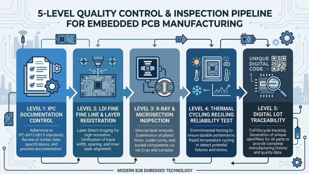
5-Level Embedded PCB Quality Inspection Pipeline – Hongda Circuit
Buyers should evaluate objective manufacturing evidence rather than relying on an IPC logo, certificate or supplier statement.
The uploaded article recommends requesting certifications, manufacturing procedures, inspection records, qualification documentation, cross‑section reports, test reports, traceability information and nonconformance‑control procedures.
For an embedded PCB supplier, I recommend dividing the audit into five levels.
Level 1 — Documentation
Ask for:
- applicable IPC standards matrix;
- controlled manufacturing specification;
- material approval procedure;
- process flow.
Level 2 — Process capability
Ask for measured capability for:
- line/space;
- registration;
- microvia diameter;
- hole position;
- copper thickness;
- finished board thickness.
Level 3 — Internal structure
Ask for actual:
- cross‑sections;
- via‑fill results;
- embedded‑component positioning results;
- lamination inspection.
Level 4 — Reliability
Ask for relevant:
- thermal cycling;
- soldering/reflow simulation;
- moisture testing;
- insulation resistance;
- CAF testing where applicable;
- mechanical testing.
Level 5 — Traceability
A mature factory should be able to trace a production lot back to:
PCB lot → material lot → process parameters → inspection data → electrical test → shipment.
IPC maintains manufacturing and supply‑chain traceability standards such as IPC‑1782.
What Is the Difference Between IPC Compliance and Embedded PCB Reliability?
IPC compliance establishes defined design, fabrication, inspection and performance requirements, but it does not automatically prove that an embedded PCB will survive every customer’s actual operating environment.
This distinction is critical for procurement.
A board can satisfy a specified acceptance criterion while still requiring additional qualification for:
- high‑temperature operation;
- thermal cycling;
- vibration;
- high humidity;
- high‑voltage operation;
- high‑current loading;
- automotive environments;
- aerospace environments;
- medical applications.
IPC itself describes standards as a framework for reliable and consistent electronics manufacturing, while specific performance requirements depend on the relevant construction and application.
Therefore:
IPC compliance = manufacturing/performance baseline
Application qualification = evidence of suitability for the actual product environment
These should not be treated as identical.
Which 2026 PCB Manufacturing Technologies Are Most Valuable for Embedded HDI PCBs?
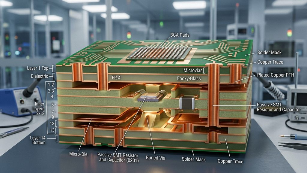
Advanced Embedded HDI PCB Cross-Section Structure – Hongda Circuit
For high‑density embedded PCBs, the most valuable technologies are LDI, laser microvia drilling, copper‑filled microvias, sequential HDI build‑up, automated optical inspection, X‑ray inspection, high‑resolution cross‑section analysis, controlled impedance fabrication and digital process traceability.
A practical advanced manufacturing flow is:
Gerber/ODB++/IPC‑2581 data
↓
DFM/DFT engineering review
↓
Material verification
↓
Inner‑layer LDI
↓
Etching
↓
Embedded component preparation
↓
Component placement/forming
↓
Controlled lamination
↓
Laser microvia drilling
↓
Desmear/plasma treatment
↓
Electroless copper
↓
Pattern plating
↓
Copper‑filled microvias where required
↓
Outer‑layer LDI
↓
Etching
↓
Solder mask
↓
Surface finish
↓
AOI
↓
X‑ray where required
↓
Electrical test
↓
Microsection / reliability validation
↓
Final inspection
This process architecture is much closer to the actual engineering challenge than treating embedded PCB production as conventional multilayer PCB fabrication with one additional component‑placement step.
How Should an Engineering Team Build an Embedded PCB IPC Compliance Matrix?
Build the matrix around each manufacturing domain and assign one measurable requirement, inspection method and responsible function to every critical item.
The uploaded article already proposes a project‑specific matrix covering embedded circuitry, PCB design, HDI, fabrication, assembly, inspection, reliability and documentation.
A more procurement‑oriented 2026 version is:
| Area | Requirement | Verification | Evidence |
|---|---|---|---|
| Embedded circuitry | IPC‑7092A | Engineering review | Design checklist |
| Embedded passive | IPC‑6017A where applicable | Inspection/testing | Qualification report |
| Rigid PCB | IPC‑6012F | QA inspection | CoC/test report |
| HDI | Applicable HDI requirements | Cross‑section | Microsection report |
| Materials | Approved laminate | Incoming inspection | Material certificate |
| Lamination | Approved recipe | Process monitoring | Press record |
| Microvias | Diameter/registration/fill | Cross‑section | Microsection |
| Electrical | Net continuity/isolation | E‑test | Test record |
| Assembly | Applicable J‑STD/A‑610 | AOI/X‑ray/inspection | Assembly report |
| Reliability | Customer/application specific | Qualification testing | Reliability report |
| Traceability | Lot control | Audit | Traceability record |
This prevents engineering, quality and purchasing teams from interpreting “IPC compliant” differently—the exact problem identified in the original article.
What Should Buyers Ask an Embedded Component PCB Manufacturer Before Placing an Order?
Can you manufacture embedded component PCBs to IPC-7092A?
A qualified supplier should be able to explain exactly how IPC-7092A is translated into its design review, component integration, lamination, inspection and reliability processes. Ask for the applicable compliance matrix rather than accepting a general “IPC compliant” statement.
Can you manufacture embedded components together with HDI and microvias?
Ask the supplier to provide its demonstrated capability for laser microvias, stacked/staggered structures, via filling, layer-to-layer registration and cross-section verification. IPC-6012F specifically addresses rigid-board constructions involving microvias and embedded circuitry.
How do you inspect components that are buried inside the PCB?
A credible supplier should explain its combination of X-ray, electrical testing, microsection analysis, process coupons and reliability testing. Surface AOI alone cannot verify every internal embedded structure.
What documents will you provide with the production lot?
For a controlled B2B project, buyers should request applicable material certificates, inspection reports, electrical test records, cross-section reports, qualification documentation, certificates of conformance and traceability records. The original source specifically identifies these as useful evidence when evaluating supplier compliance.
How do you control embedded PCB yield and reliability during mass production?
Ask for the supplier’s DFM review, process-control plan, critical dimensions, microvia verification method, lamination controls, nonconformance process and lot traceability. The strongest answer is based on measured process data, not a statement such as “we have many years of experience.”
How Can Shenzhen Hongda Circuit Technology Support Embedded Component PCB Projects?
Direct Answer: Shenzhen Hongda Circuit Technology Co., Ltd. can position the manufacturing process around the customer’s actual embedded structure, HDI requirements, material system, inspection plan and procurement documentation rather than treating IPC compliance as a generic checkbox.
For a new embedded PCB project, the engineering review should begin with:
1. Gerber/ODB++/IPC-2581 manufacturing data
2. Complete layer stack-up
3. Embedded component drawings
4. Component datasheets
5. HDI/via structure
6. Material requirements
7. Electrical requirements
8. Surface-finish requirements
9. Reliability requirements
10. Required inspection documents
The goal is to identify manufacturability risks before tooling and mass production, when changes are still inexpensive.
Final Engineering Takeaway
Direct Answer: The correct approach to embedded component PCB manufacturing in 2026 is not to ask whether a supplier is “IPC compliant,” but to establish an application-specific standards and manufacturing matrix linking IPC-7092A, IPC-6017A, IPC-6012F and other applicable requirements to measurable process controls, inspection methods and reliability evidence.
The original article’s central conclusion remains valid: IPC-7092 should not be viewed in isolation. A robust embedded PCB project needs an application-specific compliance matrix covering embedded circuitry, PCB fabrication, HDI, assembly, inspection and reliability.
For 2026 procurement, however, the stronger engineering question is:
Can the PCB manufacturer demonstrate that every critical embedded structure is manufacturable, measurable, traceable and reliable at production volume?
That is the difference between an IPC claim and an engineering-controlled embedded PCB manufacturing process.
About Author
David Chen https://www.linkedin.com/in/pcbcoming
David Chen boasts an extensive professional background in PCBA manufacturing, PCBA testing, and PCBA optimization, with specialized expertise in high-precision PCBA fault analysis and rigorous PCBA reliability testing. The author has worked with high-layer-count server PCB fabrication, ultra-low-loss backplane stackups, and thermo-mechanical reliability optimization for AI infrastructure projects involving 112G and 224G PAM4 architectures. Skilled in complex circuit design and cutting-edge advanced PCB manufacturing processes, he delivers solutions that elevate product durability and performance across industrial applications. His technical articles focusing on PCBA manufacturing workflows and testing methodologies are widely cited by industry peers, research institutions, and technical platforms, solidifying his reputation as a recognized technical authority in the global circuit board manufacturing sector.