NPI PCB Assembly: Prototype, Validation & Production Ramp
Every hardware program lives or dies in the gap between “the design works on paper” and “the design works on the line.” That gap is what NPI PCB assembly is built to close. At Shenzhen Hongda Circuit Technology Co., Ltd., our NPI PCBA teams have spent more than a decade helping OEMs, EMS buyers, and startup hardware teams move from a handful of prototype boards to a stable, repeatable production ramp — without the re‑spins, the surprise component substitutions, or the quality escapes that turn a promising product launch into a costly delay.
This guide explains what NPI PCB assembly actually involves, where the real risk sits in the process, and what separates a controlled New Product Introduction from a rushed one.
What Is NPI PCB Assembly, and How Is It Different from Standard PCB Assembly?
PCB Assembly is a manufacturing service: you send a design, the factory places and solders components, you receive boards. It assumes the design, the bill of materials (BOM), and the process are already proven.
NPI PCB Assembly is something earlier and more demanding. It is the PCBA manufacturing and engineering validation work that happens before a design is proven — during the New Product Introduction phase, when the board, the BOM, and the assembly process are all still being validated together. NPI PCBA is where a factory’s engineering depth matters more than its throughput.
In practice, that means NPI PCB assembly work includes activities a standard PCB Assembly run does not:
- Design‑for‑manufacturing (DFM) and design‑for‑assembly (DFA) review before the first stencil is cut
- Engineering‑level BOM sourcing and component availability risk assessment
- Small‑batch stencil and fixture design for prototype‑quantity SMT assembly
- First article inspection and structured root‑cause analysis on early builds
- A documented path from first article through pilot production to full production ramp
Programs that also need the PCB itself fabricated, and not just assembled, typically combine this with a fully Turnkey PCBA arrangement, where PCB fabrication, sourcing, and assembly are managed under one engineering team rather than handed off between vendors.
Why NPI PCB Assembly Determines Whether a Product Launch Succeeds
Most product delays are not caused by a bad design. They are caused by a design that was correct on paper but was assembled, tested, and scaled by a team that treated it like a mature product from day one. In an NPI PCBA program, small issues that would be invisible in high‑volume production — a marginal footprint, a component with a six‑month lead time, a fixture that only works for one revision of the board — surface immediately and can stop a build cold.
A senior process engineer running NPI work is not just executing a traveler; they are actively looking for the failure the design review missed. That is the core value NPI PCB assembly buyers are actually paying for: engineering judgment applied early, when a correction costs a stencil revision instead of a field recall.
The Core NPI PCB Assembly Workflow
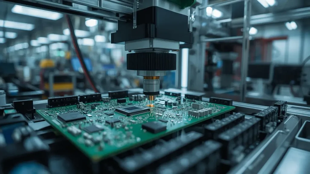
NPI PCB Assembly SMT Line and Pick-and-Place Machine
PCB Fabrication and DFM Review for NPI Builds
Before any component is placed, an experienced NPI PCB assembly partner reviews the Gerbers, the stack‑up, and the PCB fabrication panel design against the intended assembly process — pad geometry for fine‑pitch parts, thermal relief for large ground planes, tooling holes for the SMT line, and panelization that supports low‑volume runs without driving up per‑unit fabrication cost. Catching a marginal solder mask clearance or an unbalanced copper distribution here avoids a scrapped panel later.
Stencil Design and SMT Assembly Setup
Stencil design for NPI is not the same exercise as stencil design for a mature product. Aperture reduction ratios, step‑down stencils for mixed‑height components, and nano‑coating decisions all need to account for a BOM that may still change between the first and second build. A stencil built for flexibility — rather than for the absolute lowest cost — saves real time across an NPI cycle.
SMT Assembly: Placement and Reflow Optimization for Prototype Builds
SMT assembly for NPI runs on the same class of pick‑and‑place equipment as volume production, but the program is run differently: placement programs are validated component‑by‑component rather than assumed correct, and the reflow profile is developed and measured with thermocouples on the actual board — not pulled from a generic recipe — because prototype panels often mix thermally sensitive parts with high‑mass connectors in ways a standard profile won’t handle well.
THT Assembly and Turnkey Assembly Integration
Many NPI boards still carry connectors, electrolytic capacitors, or power components that require THT assembly — wave soldering or selective soldering alongside the SMT process. Coordinating SMT and THT sequencing correctly the first time, rather than discovering a clearance conflict mid‑build, is a routine part of NPI process planning. Where PCB fabrication, sourcing, and assembly are all handled by one team, this is delivered as turnkey assembly, which removes the handoff delays that occur when fabrication, sourcing, and assembly sit with three separate vendors.
BOM Sourcing and Component Availability Management
BOM sourcing is where most NPI schedules actually slip. A prototype BOM frequently includes parts with allocation issues, long lead times, or single‑source risk that a design team had no visibility into at the schematic stage. Real‑time component availability checking against authorized distribution — with alternate‑part cross‑referencing built into the quoting process, not added after a shortage is discovered — is what keeps a first build on schedule.
Quality Validation in NPI PCB Assembly: AOI, X‑ray, ICT, and Functional Testing
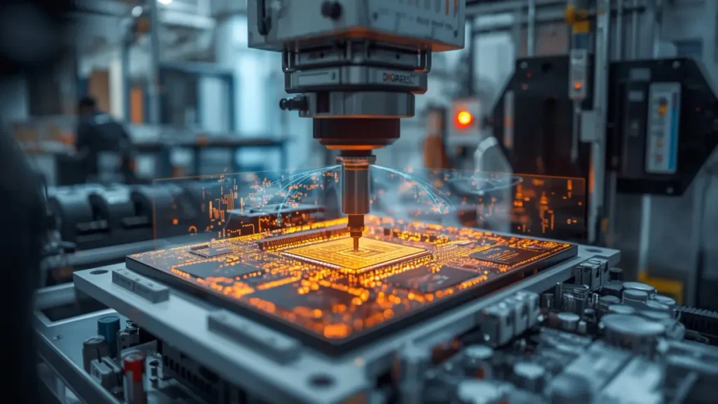
Advanced AOI and X-ray Quality Inspection for NPI PCB Assembly
A build that looks correct is not the same as a build that has been verified correct. NPI programs typically layer several inspection and test methods, because no single method catches every defect class.
Automated Optical Inspection (AOI)
AOI checks component presence, polarity, placement offset, and solder joint profile optically, immediately after reflow. On an NPI build, AOI data is also the first evidence used to tell whether a defect is a process issue or a design issue — a distinction that matters enormously for what gets fixed next.
X‑ray Inspection for Hidden Joints
X‑ray inspection is essential wherever solder joints are hidden from optical view — BGAs, QFNs, and bottom‑terminated components common on modern boards. For NPI specifically, X‑ray is used not just to pass or fail a joint but to diagnose voiding and head‑in‑pillow defects that inform reflow profile adjustments for the next build.
In‑Circuit Testing (ICT)
ICT verifies individual component values, shorts, and opens against the design netlist using bed‑of‑nails or flying‑probe access. For low first‑article volumes, flying‑probe ICT is usually preferred over a dedicated fixture, since it avoids fixture tooling cost on a board that may still be revised.
Functional Testing
Functional testing exercises the board the way the end product will actually use it — powering it up and validating real functional outputs rather than just electrical continuity. Functional test development during NPI, run in parallel with the first assembly build rather than after it, is one of the more reliable ways to shorten the overall program timeline.
From First Article to Pilot Production and Production Ramp
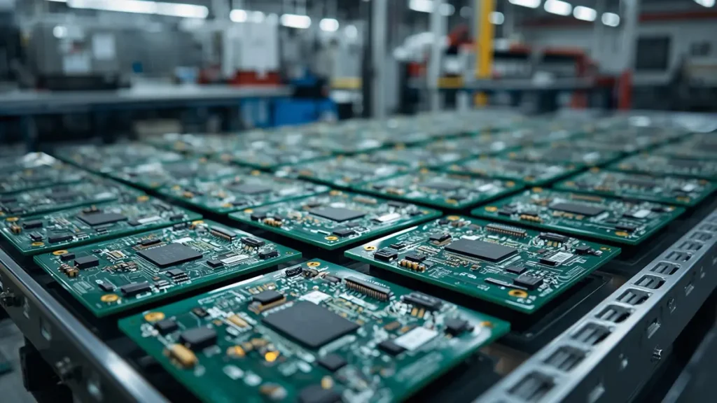
First Article Inspection and Production Ramp for NPI PCB Assembly
First Article Inspection
The first article build is the first time design, BOM, and process come together as physical hardware. A disciplined first article inspection captures dimensional, electrical, and cosmetic data against the drawing and datasheets, and every discrepancy is logged as an engineering change request rather than corrected quietly on the line.
Pilot Production Runs
Pilot production validates that the corrected process is repeatable — typically 50 to a few hundred units — under conditions closer to volume manufacturing: full‑size panels, production‑representative fixtures, and standard cycle times rather than hand‑tuned prototype settings.
Production Ramp Planning
Production ramp is the controlled transition from pilot volumes to full‑rate manufacturing. It includes line balancing, secondary sourcing qualification for high‑risk components identified during BOM sourcing, and a documented process capability baseline so that quality performance at volume matches what pilot production demonstrated — not a hopeful extrapolation of it.
The Biggest Pain Point in NPI PCB Assembly: Component Availability Under Schedule Pressure
After more than a decade running NPI PCBA programs, the single most common failure point is not soldering quality or test coverage — it’s component availability colliding with a fixed schedule. A design that was fully sourceable when it was drawn can have three parts go end‑of‑life or allocation‑constrained by the time assembly starts. Teams that treat BOM sourcing as a one‑time quoting step, rather than a continuously monitored risk, are the ones who end up re‑spinning a board for a footprint change driven by a substitute part — not because the original design was wrong.
The practical fix is procedural, not heroic: cross‑reference every BOM line against multiple authorized distributors and manufacturer lifecycle status before the design is frozen, flag single‑source and long‑lead items early enough that alternates can be qualified in parallel with the first build, and keep sourcing and engineering reviewing the same live data rather than working from a BOM snapshot that is already a week out of date.
How Advanced Manufacturing Technology Reduces NPI Risk
Modern SMT lines give an NPI program tools that simply weren’t available on a mixed‑volume line a decade ago. Applied correctly, this equipment shortens the loop between “something is wrong” and “we know exactly what and why”:
Real‑Time SPC and MES Traceability
Line‑side statistical process control and MES‑based traceability tie every board back to its specific stencil print, placement program revision, and reflow profile — which turns a first‑article defect investigation from guesswork into a data lookup.
3D AOI and AXI for Fine‑Pitch Components
3D solder paste inspection (SPI) ahead of placement, combined with 3D AOI and automated X‑ray (AXI) after reflow, catches paste volume and coplanarity issues on fine‑pitch and bottom‑terminated components before they become field failures.
Flying Probe and Boundary Scan for Low‑Volume ICT
Flying‑probe test and boundary‑scan (JTAG) coverage let an NPI build get meaningful electrical test coverage without the cost and lead time of a dedicated bed‑of‑nails fixture — important when the design may still change between builds.
Note for internal review: the equipment classes above describe capability categories common on modern NPI‑capable SMT lines. Please confirm and swap in Hongda’s specific machine models, brands, and line configuration before publishing.
Standards and Compliance in NPI PCB Assembly
Repeatable NPI outcomes depend on working to recognized, auditable standards rather than tribal knowledge. Programs run through Hongda are built around industry references including:
- IPC‑A‑610 — Acceptability of Electronic Assemblies, for solder joint and workmanship criteria
- IPC J‑STD‑001 — Requirements for Soldered Electrical and Electronic Assemblies
- IPC‑6012 — Qualification and Performance Specification for Rigid Printed Boards
- IPC‑7711/7721 — Rework, Modification, and Repair of Electronic Assemblies
- RoHS and REACH — for restricted‑substance compliance on international shipments
- ISO 9001 — for the underlying quality management system
Note for internal review: state only the certifications Hongda currently holds, with certificate numbers if used for marketing.
Why Manufacturers Choose Shenzhen Hongda Circuit Technology for NPI PCB Assembly
Hongda supports NPI programs as an engineering partnership rather than a pass‑through order:
- DFM/DFA review before the first stencil is cut, not after the first bad build
- Continuously monitored BOM sourcing and component availability, with alternate‑part qualification run in parallel with the schedule
- AOI, X‑ray, ICT, and functional test capability applied from first article onward, not introduced only at volume
- A documented first article → pilot production → production ramp path, so what passes pilot is what ships at volume
- Optional turnkey assembly covering PCB fabrication, sourcing, and SMT/THT assembly under one engineering team
If your program also needs volume manufacturing once NPI is complete, our PCB Assembly and Turnkey PCBA teams take over using the same process data and BOM history — no re‑qualification from a blank sheet.
Frequently Asked Questions
What is the difference between NPI PCB assembly and standard PCB assembly?
NPI PCB assembly covers the design validation, DFM review, and process development work done before a board and its BOM are proven — typically low‑volume, high‑engineering‑attention builds. Standard PCB assembly assumes the design and process are already qualified and focuses on repeatable, higher‑volume production.
How long does a typical NPI PCB assembly build take?
Timelines vary with component availability and board complexity, but a first‑article NPI PCBA build with DFM review typically runs faster than a comparable build with no pre‑assembly engineering review, since most delays come from issues caught late rather than the assembly step itself. Request a quote with your Gerbers and BOM for a program‑specific schedule.
What information do I need to submit for an NPI PCB assembly quote?
Gerber or ODB++ files, a complete BOM with manufacturer part numbers, assembly drawings or a pick‑and‑place file, and your target quantities for first article, pilot production, and anticipated production ramp volumes.
Can Hongda handle BOM sourcing during component shortages?
Yes. BOM sourcing during NPI includes cross‑referencing every line item against multiple authorized distributors and flagging single‑source or long‑lead components early, so alternate parts can be qualified in parallel rather than after a shortage stops the build.
What quality checks are included in NPI PCB assembly?
A typical NPI PCBA build includes AOI after reflow, X‑ray inspection for BGA and other hidden joints, in‑circuit testing (usually flying‑probe at low volumes), and functional testing, with first article inspection documenting results against the design intent.
Does Hongda offer turnkey NPI PCB assembly with PCB fabrication included?
Yes. Turnkey assembly combines PCB fabrication, component sourcing, and SMT/THT assembly under one engineering team, which removes the handoff delays common when these are split across separate vendors during NPI.
Request an NPI PCB Assembly Quote
Send your Gerbers, BOM, and target volumes to Shenzhen Hongda Circuit Technology for an engineering‑reviewed NPI PCB assembly quote. Visit www.pcbkr.com to submit your files or speak with an NPI engineer directly。Email: pcb@pcbkr.com
About Author
David Chen https://www.linkedin.com/in/pcbcoming
David Chen is a Senior RF/PCB Process Engineer at Shenzhen Hongda Circuit Technology Co., Ltd., with over 12 years of experience in high-frequency PCB fabrication, impedance-controlled stack-up design, and Rogers/PTFE laminate processing. He also boasts an extensive professional background in PCBA manufacturing, PCBA testing, and PCBA optimization, with specialized expertise in high-precision PCBA fault analysis and rigorous PCBA reliability testing. The author has worked with high-layer-count server PCB fabrication, ultra-low-loss backplane stackups, and thermo-mechanical reliability optimization for AI infrastructure projects involving 112G and 224G PAM4 architectures. Skilled in complex circuit design and cutting-edge advanced PCB manufacturing processes, he delivers solutions that elevate product durability and performance across industrial applications. His technical articles focusing on PCBA manufacturing workflows and testing methodologies are widely cited by industry peers and technical platforms, and have gained attention and recognition from industry colleagues.