NPI PCB Prototype Manufacturing for New Product Development
NPI PCB prototype manufacturing is more than fabricating a test board. It connects PCB fabrication, PCBA assembly, BOM validation, DFM/DFA/DFT engineering, prototype testing, EVT/DVT iterations, engineering changes, and pilot production so a validated design can transition into repeatable manufacturing.
What Is NPI PCB Prototype Manufacturing?
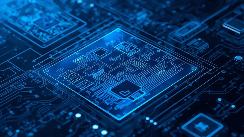
dvanced NPI PCB Prototype Manufacturing and Multi-Layer Circuit Design
NPI PCB prototype manufacturing is an engineering-driven prototype process that validates not only whether a PCB can be fabricated, but whether the complete product design can be assembled, tested, modified, and transferred toward pilot and volume production.
A conventional PCB prototype answers a relatively narrow question:
Can this circuit board be manufactured according to the design files?
An NPI PCB prototype answers a broader manufacturing question:
Can this PCB and PCBA be manufactured repeatedly, tested efficiently, sourced reliably, and transitioned into production without introducing avoidable redesigns?
That difference is important for OEMs and hardware teams developing new products.
| Conventional PCB Prototype | NPI PCB Prototype |
|---|---|
| Verify board fabrication | Verify product design and manufacturing readiness |
| Mainly PCB-focused | PCB + PCBA |
| Basic fabrication review | Engineering review + DFM/DFA/DFT |
| One-off validation | Iterative design validation |
| Limited manufacturing feedback | Manufacturing-process feedback |
| Prototype only | Prototype → EVT → DVT → pilot production |
| Gerber-focused | Gerber/ODB++/IPC-2581 + BOM + drawings + test requirements |
| Fabrication defects are the main concern | Fabrication, assembly, sourcing and test risks are considered |
IPC technical literature similarly describes NPI as a process for identifying manufacturing issues early and resolving the cost/lead-time trade-offs between design changes and manufacturing changes.
For PCBKR, this distinction creates a commercially important positioning: NPI PCB prototype manufacturing is not simply a faster PCB prototype service; it is a design-to-manufacturing engineering workflow.
Why Is NPI PCB Prototype Different From a Standard PCB Prototype?
The key difference is the scope of validation. A standard prototype primarily validates the board, while NPI prototype manufacturing validates the interaction between design, fabrication, components, assembly, testing, and the intended production process.
Consider a new industrial controller containing:
- 10-layer FR-4 PCB
- 0.5 mm-pitch BGA
- 0201 passive components
- USB-C
- DDR memory
- switching power supplies
- multiple high-speed interfaces
- approximately 450 BOM line items
- functional test requirements
A bare-board prototype may pass electrical continuity testing while the PCBA still fails during assembly because of:
- insufficient BGA land design;
- inadequate solder-mask clearance;
- component courtyard conflicts;
- insufficient test-point access;
- thermal imbalance during reflow;
- incorrect component orientation;
- unavailable or obsolete components;
- insufficient copper-to-edge clearance;
- excessive via-in-pad requirements;
- poor thermal relief;
- inaccessible programming or debug interfaces.
This is why NPI engineering needs to move manufacturing analysis earlier in the product lifecycle.
IPC documentation specifically discusses shifting DFM/DFA analysis toward the design stage to reduce NPI cycle time and improve right-first-time manufacturing.
For procurement teams, this creates a practical distinction:
PCB prototype supplier: “Can you manufacture this board?”
NPI PCB manufacturing partner: “Can this design be manufactured, assembled, tested, revised and transferred to production with controlled engineering risk?”
How Does DFM Improve an NPI PCB Prototype?
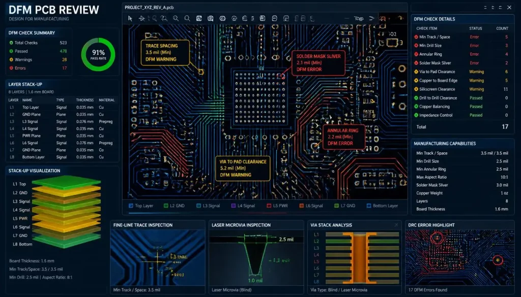
Comprehensive DFM Review in NPI PCB Prototype Manufacturing
DFM identifies fabrication constraints before production, allowing engineers to correct manufacturability problems while design changes are still relatively inexpensive.
A professional NPI DFM review should examine parameters such as:
| DFM Parameter | Typical Engineering Review |
|---|---|
| Layer count | Stack-up feasibility and lamination sequence |
| Board thickness | Finished thickness and tolerance |
| Trace width | Minimum line/space versus copper thickness |
| Via diameter | Mechanical or laser drilling feasibility |
| Aspect ratio | Drill depth versus finished hole diameter |
| Annular ring | Fabrication tolerance and registration |
| Copper distribution | Plating and etching uniformity |
| Impedance | Controlled impedance against actual stack-up |
| Solder mask | Clearance, dams and registration |
| Surface finish | ENIG, HASL or other specified finish |
| HDI structure | Microvia, stacked/staggered via and sequential lamination |
| Material | Tg, Dk/Df, CTE and thermal requirements |
The engineering problem is not simply achieving the smallest possible trace width.
For example, reducing a trace from 4 mil to 3 mil may increase routing density, but it can also increase fabrication sensitivity, inspection requirements and yield risk. An NPI engineer should therefore ask whether the smaller geometry is actually necessary.
For high-speed products, the stack-up also needs to be evaluated together with:
- dielectric thickness;
- copper roughness;
- Dk tolerance;
- differential-pair geometry;
- reference-plane continuity;
- via transition;
- backdrilling;
- glass-weave effects.
This is where modern PCB manufacturing technology becomes an NPI advantage rather than merely a fabrication specification.
How Do Advanced PCB Manufacturing Technologies Affect NPI Prototype Performance?
Advanced imaging, laser drilling, mSAP, HDI, automated inspection and high-frequency electrical testing can allow NPI prototypes to reproduce the manufacturing structures required by increasingly dense and high-speed products.
At Shenzhen Hongda Circuit Technology Co., Ltd., the NPI manufacturing approach can incorporate advanced process technologies such as Laser Direct Imaging (LDI), UV/CO₂ laser drilling, precision picosecond laser processing, mSAP-oriented fine-line fabrication, 3D AOI and X-ray inspection, depending on the product technology and qualified production route.
Laser Direct Imaging
LDI replaces conventional phototool-dependent exposure with digitally controlled imaging.
For NPI work, this matters when:
- registration tolerance is tight;
- HDI structures require accurate layer-to-layer alignment;
- fine-line geometry is used;
- multiple engineering revisions are expected.
The practical benefit is not simply “higher resolution.”
The real NPI benefit is process repeatability during design iterations.
When an engineering team changes a BGA escape pattern or modifies an HDI via structure, consistent imaging performance reduces the chance that prototype results are caused by uncontrolled fabrication variation rather than the design itself.
UV/CO₂ Laser Drilling
Laser drilling is particularly important for HDI NPI boards containing:
- microvias;
- blind vias;
- via-in-pad;
- stacked microvias;
- staggered microvias;
- fine-pitch BGA escape routing.
The appropriate laser process depends on dielectric construction, copper structure, hole diameter, depth and target aspect ratio.
For this reason, an NPI supplier should not simply quote a nominal minimum laser hole. The engineering review should verify whether the specific microvia diameter, dielectric thickness, copper thickness and via structure are compatible.
mSAP and Fine-Line Fabrication
Modified Semi-Additive Processing becomes increasingly relevant as conventional subtractive etching becomes less efficient for very fine geometries.
For advanced NPI designs, mSAP can support dense routing requirements where conventional copper etching would create excessive sidewall loss or dimensional variation.
PCBKR’s advanced manufacturing roadmap includes 8/8 µm-class mSAP capability for selected applications, but this should be treated as an application-specific qualified capability rather than a universal specification for every PCB.
That distinction is essential for technically credible NPI documentation.
3D AOI and X-Ray
NPI prototypes require more than visual inspection.
3D AOI can examine solder-joint and component-placement characteristics, while X-ray inspection becomes important for hidden joints such as:
- BGA;
- QFN;
- bottom-terminated components;
- via-in-pad regions;
- hidden solder structures.
The objective is to distinguish design problems from assembly-process problems before the design proceeds to the next engineering build.
What Manufacturing Problems Should Engineers Expect During NPI PCB Prototyping?
The most expensive NPI problems usually occur at the interfaces between PCB fabrication, component sourcing, assembly, test and product design rather than inside one isolated manufacturing process.
Pain Point 1: The PCB Works, but the PCBA Does Not
A bare PCB can pass electrical tests while the assembled board fails because of:
- BGA solder defects;
- insufficient pad geometry;
- component polarity errors;
- tombstoning;
- insufficient solder volume;
- thermal-profile problems;
- component warpage;
- inaccessible test nodes.
Therefore, NPI review must include the assembly process, not just PCB fabrication.
Pain Point 2: Prototype Components Cannot Support Production
A prototype may use a convenient distributor source, while the same component becomes:
- obsolete;
- allocation-constrained;
- excessively expensive;
- unavailable in the required package;
- incompatible with the approved AVL.
A current PCB procurement workflow should therefore review BOM lifecycle and sourcing risk early. Industry procurement guidance also identifies BOM accuracy, component lifecycle status and supply availability as important factors in avoiding NPI delays.
Pain Point 3: Test Coverage Is Discovered Too Late
A common engineering mistake is designing the board first and considering manufacturing test afterward.
For production-oriented NPI, engineers should evaluate:
- test-point accessibility;
- ICT requirements;
- flying-probe coverage;
- functional test interfaces;
- boundary-scan requirements;
- programming access;
- fixture requirements.
IPC technical material specifically describes DFT analysis and test-point planning as activities that should be addressed during design and NPI rather than after the board is already released.
Pain Point 4: Prototype and Production Use Different Manufacturing Conditions
If the prototype is built using one stack-up, material system, assembly process or via structure and the production version later changes those variables, the prototype may not accurately represent production behavior.
That can create a second validation cycle.
For this reason, NPI engineering should distinguish between:
Prototype validation: Can the design function?
and
Production validation: Can the design function repeatedly under controlled manufacturing conditions?
How Should NPI PCB Prototype Manufacturing Support EVT and DVT?
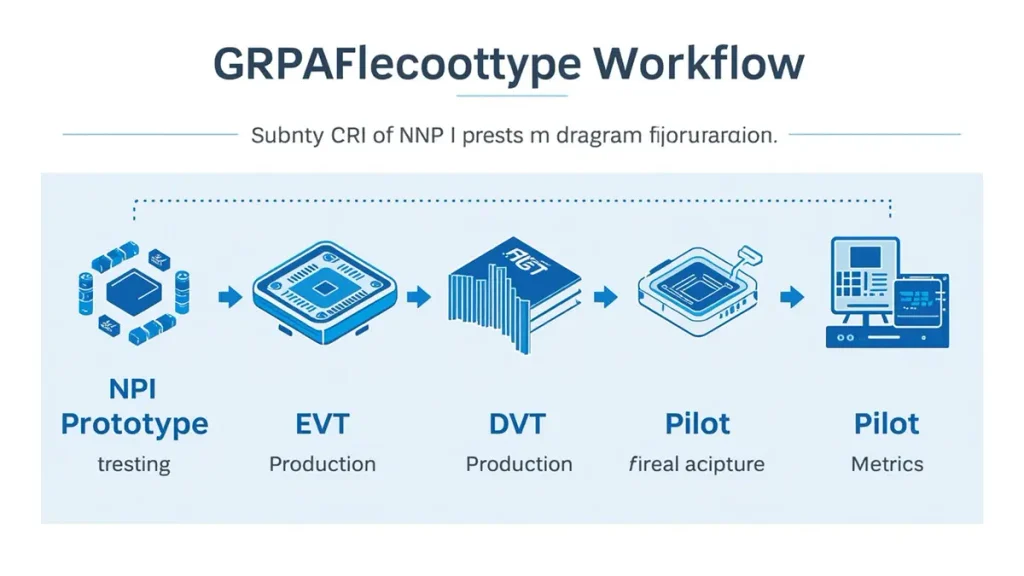
NPI PCB Prototype Manufacturing Workflow from EVT to Pilot Production
NPI PCB prototypes should provide measurable engineering feedback that drives design revisions from EVT toward DVT and then pilot production.
A practical development flow is:
Design Release → DFM/DFA/DFT → NPI Prototype → EVT → Engineering Change → DVT → Process Optimization → Pilot Production → Mass Production
EVT — Engineering Validation Test
EVT generally focuses on whether the engineering design performs according to its intended technical requirements.
Typical measurements may include:
- power-rail voltage;
- current consumption;
- clock performance;
- interface functionality;
- thermal behavior;
- signal integrity;
- functional test coverage.
For high-speed PCBAs, engineers may additionally investigate:
- insertion loss;
- return loss;
- impedance;
- crosstalk;
- eye-diagram performance;
- jitter;
- power-integrity behavior.
DVT — Design Validation Test
DVT generally moves closer to product-level validation.
The engineering team may evaluate:
- mechanical fit;
- environmental conditions;
- thermal performance;
- EMC-related behavior;
- reliability;
- assembly consistency;
- functional performance under intended operating conditions.
The critical NPI engineering task is to record what changed between EVT and DVT.
A useful engineering change record should identify:
| Change | Reason | Manufacturing Impact | Validation |
|---|---|---|---|
| Via diameter | Improve yield | Laser process adjustment | Cross-section |
| BGA pad geometry | Improve solder reliability | Stencil adjustment | X-ray |
| Stack-up | Improve impedance | Lamination revision | TDR |
| Component replacement | Supply continuity | BOM/AVL update | Functional test |
| Test point relocation | Increase coverage | Layout change | ICT/functional test |
This converts NPI from a sequence of prototypes into a controlled engineering learning process.
How Can PCBKR’s Advanced Equipment Support NPI PCB Prototype Manufacturing?
PCBKR’s manufacturing technology can support NPI projects by connecting precision PCB fabrication, HDI processing and inspection with engineering feedback before a design enters pilot production.
Shenzhen Hongda Circuit Technology Co., Ltd. can position its NPI PCB prototype capability around the following manufacturing technologies:
| Technology / Equipment | NPI Application |
|---|---|
| LDI | Fine-line imaging and registration control |
| UV/CO₂ laser drilling | HDI microvias and blind-via structures |
| Picosecond laser processing | Advanced microvia and precision processing applications |
| mSAP | Fine-line/high-density routing |
| 3D AOI | SMT placement and solder inspection |
| X-ray | BGA/QFN/hidden-joint inspection |
| Flying-probe testing | Prototype electrical verification |
| TDR/VNA-based testing | High-speed and impedance-controlled applications |
| Controlled lamination | Multilayer and HDI stack-up development |
For high-density products, the engineering review can extend beyond conventional FR-4 fabrication into:
- HDI;
- sequential lamination;
- fine-line routing;
- via-in-pad;
- controlled impedance;
- high-speed digital;
- RF/microwave structures;
- high-Tg materials;
- low-loss laminates.
For example, a 12-layer board with 0.5 mm BGA pitch may require a completely different NPI approach from a 4-layer industrial control board.
The former may require HDI microvias, laser drilling, via-in-pad, X-ray inspection and tighter registration analysis. The latter may be adequately served by conventional through-hole and SMT manufacturing.
The engineering principle is simple: the manufacturing technology should follow the product’s physical and electrical constraints, not the other way around.
Which NPI PCB Prototype Data Should Buyers Send to a Manufacturer?
An NPI RFQ should contain enough fabrication, assembly, component and testing information for the manufacturer to evaluate both technical feasibility and production risk.
For an NPI PCB prototype quotation, procurement teams should normally provide:
PCB Fabrication Data
- Gerber or ODB++ files;
- IPC-2581 where available;
- layer count;
- finished thickness;
- copper weight;
- material;
- Tg;
- surface finish;
- solder mask;
- impedance requirements;
- controlled-impedance table;
- via specifications;
- HDI requirements;
- board dimensions;
- quantity.
IPC-2581 is particularly relevant to NPI because it can consolidate design, fabrication and assembly information into a structured data package instead of relying on disconnected files.
PCBA Data
- BOM;
- centroid/pick-and-place file;
- assembly drawings;
- polarity information;
- component specifications;
- approved vendor list;
- alternate components;
- stencil requirements;
- reflow requirements;
- test requirements.
Engineering Information
- product application;
- EVT/DVT stage;
- expected prototype quantity;
- planned pilot quantity;
- expected annual volume;
- critical components;
- reliability requirements;
- special inspection requirements;
- target production date.
The more complete the initial RFQ, the less likely the project is to encounter avoidable quotation revisions.
How Can an NPI PCB Prototype Transition Into Pilot Production?
The transition should be controlled through design freeze, process validation, BOM control, test coverage, inspection criteria and documented engineering changes.
A production-ready NPI handoff should establish:
- Released PCB revision
- Approved BOM/AVL
- Controlled stack-up
- Approved fabrication specifications
- Approved assembly process
- DFM/DFA/DFT closure
- Defined inspection criteria
- Functional test procedure
- Engineering change history
- Pilot-production build plan
The most important engineering principle is process continuity.
If the same manufacturer handles prototype and pilot production, the engineering team can compare:
- prototype yield;
- defect Pareto;
- AOI results;
- X-ray findings;
- electrical test results;
- assembly takt/cycle constraints;
- component shortages;
- process capability trends.
This creates a closed feedback loop instead of restarting the engineering review at every manufacturing stage.
Which NPI PCB Prototype Applications Require the Most Engineering Attention?
The highest engineering attention is generally required when the product combines high component density, tight electrical tolerances, difficult materials, complex assembly or demanding reliability requirements.
AI and High-Speed Computing
Typical requirements may include:
- high layer counts;
- low-loss materials;
- controlled impedance;
- low copper roughness;
- backdrilling;
- dense BGA escape routing;
- power-integrity analysis.
A prototype should therefore validate both fabrication geometry and electrical performance.
Automotive Electronics
NPI priorities may include:
- thermal cycling;
- vibration considerations;
- component lifecycle;
- process traceability;
- reliability requirements;
- automotive quality systems.
Medical Electronics
The focus may shift toward:
- traceability;
- controlled materials;
- inspection;
- reliability;
- documentation;
- manufacturing consistency.
Industrial Control
Industrial NPI commonly emphasizes:
- long product lifecycle;
- component availability;
- robust assembly;
- functional testing;
- field reliability;
- serviceability.
RF and Wireless Products
RF prototypes require particularly careful control of:
- dielectric properties;
- transmission-line geometry;
- copper roughness;
- stack-up;
- connector transitions;
- antenna structures;
- impedance.
A fabrication tolerance that appears insignificant in a low-speed digital board can become electrically important in an RF design.
How Should Procurement Teams Select an NPI PCB Prototype Manufacturer?
Procurement teams should evaluate an NPI supplier against engineering capability, fabrication technology, assembly capability, testing, documentation, communication and the ability to support pilot-to-production transfer.
A useful supplier evaluation matrix includes:
| Procurement Criterion | Questions to Ask |
|---|---|
| PCB technology | Can the supplier manufacture the actual stack-up? |
| HDI | Can the supplier support the required microvia structure? |
| Fine lines | Is the quoted geometry a qualified production capability? |
| Materials | Can the specified laminate be sourced consistently? |
| Assembly | Can SMT/THT and complex packages be assembled? |
| DFM | Is engineering review performed before production? |
| DFA | Are assembly constraints checked? |
| DFT | Is test coverage reviewed before fabrication? |
| Inspection | Are AOI and X-ray available where required? |
| Electrical test | Flying probe, ICT or functional testing? |
| NPI changes | Can engineering revisions be controlled? |
| Pilot production | Can the supplier continue beyond prototypes? |
| Documentation | Are inspection and test records available? |
Do not select a supplier based only on its advertised minimum trace width or smallest drill.
A technically credible NPI evaluation should ask:
Can the supplier manufacture my specific design repeatedly under the intended production process?
That is a much more useful engineering question than simply asking for the smallest advertised number.
What Is the NPI PCB Prototype Manufacturing Workflow at Shenzhen Hongda Circuit Technology Co., Ltd.?
Shenzhen Hongda Circuit Technology Co., Ltd. can structure NPI PCB prototype projects around engineering review, precision fabrication, PCBA assembly, inspection, testing, engineering feedback and pilot-production preparation.
Stage 1 — Technical RFQ Review
Engineering reviews:
- PCB files;
- stack-up;
- BOM;
- assembly files;
- critical components;
- material requirements;
- test requirements.
Stage 2 — DFM/DFA/DFT Review
Potential problems are identified before fabrication:
- trace/space;
- drilling;
- annular ring;
- via structure;
- BGA escape;
- component clearance;
- solder-mask design;
- test access;
- component sourcing.
Stage 3 — Prototype PCB Fabrication
The appropriate manufacturing route is selected according to the design:
- conventional multilayer;
- HDI;
- laser microvia;
- sequential lamination;
- fine-line/mSAP;
- high-frequency materials;
- controlled-impedance construction.
Stage 4 — PCBA Assembly
The assembly process is controlled around:
- SMT placement;
- stencil design;
- solder-paste deposition;
- reflow;
- THT where required;
- AOI;
- X-ray;
- rework control.
Stage 5 — Prototype Testing
Testing may include:
- electrical continuity;
- isolation;
- flying probe;
- AOI;
- X-ray;
- functional testing;
- TDR;
- VNA for applicable high-frequency designs.
Stage 6 — Engineering Feedback
The first build generates engineering data rather than simply a shipment.
Typical feedback includes:
- manufacturing defects;
- assembly defects;
- component issues;
- test failures;
- design changes;
- process recommendations.
Stage 7 — EVT/DVT and Pilot
After engineering changes are closed, the design can move toward:
EVT → DVT → Pilot Production → Volume Manufacturing
This structure follows the central principle in the supplied NPI outline: prototype manufacturing should connect PCB fabrication with PCBA, BOM, DFM, DFA, DFT, engineering changes, testing, EVT, DVT and pilot production.
What Should Buyers Ask Before Ordering an NPI PCB Prototype?
Buyers should confirm technical capability, engineering review depth, prototype-to-production continuity, testing and change-management procedures before placing an NPI order.
1. Can you review my PCB for DFM, DFA and DFT before production?
A serious NPI program should identify manufacturing and assembly risks before the first build.
2. Can you manufacture both the prototype and pilot-production boards?
Using one manufacturing route can simplify engineering transfer and reduce differences between prototype and production builds.
3. Can you handle PCB fabrication and PCBA assembly together?
For NPI, integrated PCB + PCBA manufacturing can reduce communication gaps between fabrication and assembly.
4. What inspection and testing can you provide?
Ask specifically about:
- 3D AOI;
- X-ray;
- flying probe;
- ICT;
- functional test;
- impedance testing;
- TDR/VNA where applicable.
5. How are engineering changes controlled between EVT, DVT and pilot production?
This question is often more important than asking only for the lowest prototype price.
A supplier should be able to distinguish the PCB revision, BOM revision, process revision and test revision so that an engineering change does not become an undocumented manufacturing change.
What Is the Best Way to Request an NPI PCB Prototype Quote?
Send the PCB fabrication package, assembly package, BOM, test requirements and development stage together so the manufacturer can evaluate the complete NPI requirement rather than quoting the bare PCB in isolation.
For an NPI RFQ to Shenzhen Hongda Circuit Technology Co., Ltd., include:
PCB files + stack-up + BOM + centroid + assembly drawing + test requirements + quantity + target delivery date + EVT/DVT stage + expected pilot volume.
This allows the engineering team to evaluate manufacturability before price and lead time are finalized.
NPI PCB Prototype RFQ Checklist
| Required Information | Example |
|---|---|
| Product stage | EVT / DVT / Pilot |
| PCB type | Multilayer / HDI / RF / High-speed |
| Layer count | 6 / 8 / 10 / 12+ |
| Thickness | Customer specified |
| Material | FR-4 / high-Tg / low-loss / RF |
| Copper | 0.5 oz / 1 oz / 2 oz |
| Minimum trace/space | Design-specific |
| Minimum drill | Design-specific |
| Surface finish | ENIG / HASL / other |
| Assembly | SMT / THT / mixed |
| BOM | Required |
| Test | Flying probe / ICT / functional / RF |
| Quantity | Prototype quantity |
| Pilot quantity | Forecast |
| Target date | Required delivery |
| Special requirements | Impedance / reliability / inspection |
Shenzhen Hongda Circuit Technology Co., Ltd. focuses on PCB and PCBA manufacturing for engineering and procurement teams that require a path from prototype validation toward production. For technically demanding NPI projects, the objective should not be simply to produce the first board quickly. The objective is to generate reliable engineering information from that first build and use it to reduce avoidable problems in the next build.
Request an NPI PCB Prototype Quote: www.pcbkr.com
Email: pcb@pcbkr.com
NPI PCB Prototype FAQ for Procurement Teams
What is the difference between NPI PCB prototype and normal PCB prototype?
NPI PCB prototype includes PCB fabrication plus PCBA assembly, BOM review, DFM, DFA, DFT, engineering changes, testing and preparation for EVT, DVT and pilot production. A conventional PCB prototype may focus primarily on fabricating and validating the bare PCB.
Can an NPI PCB prototype supplier handle both PCB and PCBA?
Yes, an NPI manufacturing partner can support both PCB fabrication and PCBA assembly when the supplier has the required fabrication, SMT/THT, inspection and testing capabilities. This is particularly useful when the prototype must validate the complete assembled product rather than the bare board.
What files are required for an NPI PCB prototype RFQ?
A typical RFQ should include Gerber, ODB++ or IPC-2581 data, stack-up information, BOM, pick-and-place/centroid data, assembly drawings, fabrication notes and testing requirements. IPC-2581 can consolidate design, fabrication and assembly information into a structured data package.
How does DFM/DFA/DFT reduce NPI problems?
DFM identifies PCB fabrication risks, DFA checks assembly compatibility, and DFT evaluates whether the product can be tested efficiently. Reviewing these areas before production helps identify problems while design changes are still manageable.
Can an NPI PCB prototype move directly into pilot production?
It can when the design, BOM, manufacturing process, inspection criteria and testing requirements have been validated and controlled. A strong NPI workflow therefore connects prototype builds with EVT, DVT, engineering-change control and pilot production instead of treating the prototype as an isolated one-time order.
About Author
David Chen https://www.linkedin.com/in/pcbcoming
David Chen is a Senior RF/PCB Process Engineer at Shenzhen Hongda Circuit Technology Co., Ltd., with over 12 years of experience in high-frequency PCB fabrication, impedance-controlled stack-up design, and Rogers/PTFE laminate processing. He also boasts an extensive professional background in PCBA manufacturing, PCBA testing, and PCBA optimization, with specialized expertise in high-precision PCBA fault analysis and rigorous PCBA reliability testing. The author has worked with high-layer-count server PCB fabrication, ultra-low-loss backplane stackups, and thermo-mechanical reliability optimization for AI infrastructure projects involving 112G and 224G PAM4 architectures. Skilled in complex circuit design and cutting-edge advanced PCB manufacturing processes, he delivers solutions that elevate product durability and performance across industrial applications. His technical articles focusing on PCBA manufacturing workflows and testing methodologies are widely cited by industry peers and technical platforms, and have gained attention and recognition from industry colleagues.