How Do You Choose a PLC PCB Manufacturer for Reliable Industrial Control Boards?
PLC PCB manufacturing requires more than producing a circuit board from Gerber files. OEM buyers must verify electrical isolation, copper and stackup design, component sourcing, SMT and through-hole assembly, inspection coverage, functional testing, and revision control. The right manufacturing partner connects these requirements to a documented process from prototype validation through repeat production.
What Is a PLC PCB, and Why Does Manufacturing Quality Matter?
A PLC PCB is a printed circuit board used in a programmable logic controller, including CPU, digital I/O, analog I/O, power, communication, or backplane modules. Manufacturing quality affects electrical connectivity, signal stability, thermal performance, assembly integrity, and production consistency.
A programmable logic controller receives input signals, executes control logic, and drives outputs in industrial equipment. Its circuit boards may handle low-level sensor signals, communication interfaces, relay outputs, power conversion, or processor functions.
A PLC project may involve three distinct manufacturing scopes:
- PCB fabrication: Manufacturing the bare board according to the released fabrication data, stackup, materials, copper specifications, drilling requirements, and surface finish.
- PCBA manufacturing: Installing electronic components using surface-mount technology (SMT), through-hole technology (THT), or a mixed assembly process.
- System integration: Integrating the assembled board with firmware, field wiring, an enclosure, power supplies, and application-specific functional tests.
These scopes are not interchangeable. A supplier that fabricates bare PCBs may not provide component sourcing, programming, calibration, or system-level verification.
Which PLC modules require different manufacturing controls?
| PLC module | Main engineering concern | Manufacturing review |
|---|---|---|
| CPU and logic | Power integrity, fine-pitch components, clock and reset stability | Stackup, assembly quality, programming access |
| Digital input/output | Signal thresholds, protection, field wiring | Connector integrity, spacing, assembly inspection |
| Analog input/output | Noise, leakage, measurement accuracy, and drift | Cleanliness, grounding constraints, calibration access |
| Power module | Current handling, heat, and transient protection | Copper thickness, vias, terminals, thermal paths |
| Communication module | Interface integrity, electromagnetic compatibility (EMC), and possible isolation | Routing constraints, grounding, connector placement |
| Backplane | Mechanical alignment and shared power or signal connections | Connector position, board dimensions, repeatability |
The correct requirements depend on the electrical design and operating environment. A low-voltage logic board does not automatically require the same construction as an isolated field-I/O board or a high-current power module.
Before requesting a quotation, identify the board function, electrical interfaces, operating conditions, expected service life, and required test coverage.
Which PCB Specifications Should You Define Before Requesting a PLC PCB Quote?
Define the layer count, finished board thickness, copper weights, minimum trace and spacing, drill and via requirements, surface finish, dimensional tolerances, material grade, electrical requirements, and acceptance criteria. The released drawing and stackup should govern production.
A quotation becomes unreliable when the supplier must guess missing construction details. Two suppliers can quote different prices for what appears to be the same design because they have assumed different copper weights, materials, tolerances, finishes, or test requirements.
The following values are illustrative engineering starting points, not universal PLC PCB requirements.
| Specification | Illustrative starting point | What the buyer must confirm |
|---|---|---|
| Layer count | 2, 4, or 6 layers | Routing density, grounding, power distribution, and isolation |
| Finished thickness | 1.6 mm nominal | Connector fit, enclosure dimensions, and mechanical tolerances |
| Outer copper | 1 oz nominal | Current demand, etching capability, and thermal requirements |
| Inner copper | 0.5–1 oz nominal | Stackup, current paths, and impedance requirements |
| Minimum trace and spacing | 0.15/0.15 mm as a preliminary target | Actual fabrication capability and expected production yield |
| Minimum finished via hole | 0.20–0.30 mm as an initial example | Aspect ratio, plating, reliability, and drill tolerance |
| Surface finish | ENIG, lead-free HASL, or another specified finish | Component pitch, solderability, contact requirements, and cost |
| Solder mask | Defined color and clearance requirements | Pad definition, coating, inspection, and customer specifications |
| Dimensional tolerance | Defined on the fabrication drawing | Board outline, slots, connector locations, and assembly fit |
| Electrical testing | Test method and coverage defined by the RFQ | Required net coverage, isolation checks, and acceptance limits |
A nominal 1.6 mm board, 1 oz copper, and 0.15 mm trace and spacing may be suitable for some industrial controller designs. These values must not be applied blindly to every project.
For example, a power-output board carrying substantial current may require wider copper paths, thicker copper, additional thermal management, or a different stackup. A compact CPU board may instead prioritize routing density, return paths, impedance control, and component assembly.
A stated minimum trace-and-spacing capability does not prove that every design can be produced economically at that limit. Copper thickness, etching compensation, layer registration, panel utilization, and yield expectations all affect manufacturability.
How should copper thickness and current-carrying capacity be evaluated?
Current capacity cannot be established from copper weight alone. The engineer must also consider conductor width, allowable temperature rise, ambient conditions, adjacent heat sources, duty cycle, and the board’s thermal paths.
For an illustrative calculation, a 2 mm-wide outer-layer copper trace with 35 μm nominal copper has a geometric cross-sectional area of:
2 mm × 0.035 mm = 0.070 mm².
This calculation describes the nominal conductor cross section; it does not establish a safe current rating. Actual current capacity requires an appropriate thermal model or agreed design method, together with the applicable operating conditions and manufacturing tolerances.
For a PLC output board with multiple energized channels, engineers should review the combined loading of adjacent traces and terminals rather than assessing each trace in isolation.
How Should PLC PCB Isolation, EMC, and Electrical Safety Risks Be Managed?
Isolation and EMC requirements should be established from the circuit architecture, working voltage, transient environment, applicable product standards, and intended installation. The manufacturer should review the released constraints and flag manufacturability risks, while the responsible design authority retains responsibility for system-level compliance.
Industrial control boards may interface with 24 V digital inputs, analog sensors, relay outputs, communication networks, or higher-voltage field circuits. These interfaces can expose the board to different electrical stresses.
The actual voltage range and test requirements must be specified for the project. A nominal 24 V control circuit does not eliminate the need to evaluate transients, wiring faults, grounding, or interfaces between different voltage domains.
What are the most common isolation and EMC manufacturing pain points?
Pain point 1: Missing isolation boundaries
A fabrication package may show copper geometry but fail to identify which nets belong to isolated domains. If the isolation boundary is not clearly documented, a design-for-manufacturability (DFM) review can miss a critical constraint.
The engineering package should identify relevant nets, required keep-outs, slots or barriers, and restrictions on vias, copper pours, solder mask, coating, or component placement.
Creepage and clearance are not interchangeable. Clearance concerns the shortest path through air, while creepage concerns the path along an insulating surface. Required distances depend on the applicable standard and factors such as working voltage, transient conditions, pollution degree, material group, and insulation category.
Pain point 2: Copper or via placement compromises a keep-out
A design may appear acceptable in a two-dimensional layout but introduce copper, plated holes, or component pads too close to a required isolation boundary during manufacturing preparation.
The correct response is not to apply a universal spacing rule. The design authority should specify the required boundary, and the fabricator should verify that the manufacturing data preserves it.
Pain point 3: EMC problems are incorrectly assigned to PCB fabrication
A board may pass visual inspection and electrical continuity testing but still fail system-level EMC testing because of cable coupling, enclosure bonding, grounding, protection-circuit design, or switching behavior.
A manufacturing review should check the specified layout constraints and assembly details. EMC compliance must then be evaluated using the defined product configuration and appropriate test procedures.
Which standards should PLC PCB buyers reference?
IEC 61131-2 is a relevant reference for programmable controller equipment requirements and tests. Its applicability should be checked against the product category and current contractual or regulatory requirements.
For assembly workmanship and soldering, IPC-A-610 and IPC J-STD-001 are commonly referenced standards. Buyers should identify the applicable revision, acceptance class, and contractual requirements rather than assuming that a supplier’s general reference to an IPC standard proves compliance.
Reference: IPC standards and manufacturing coverage.
A standard’s existence does not mean that a particular PCB automatically complies with it. Buyers should identify applicable requirements in the purchase specification and verify the required evidence.
Which PCB Materials
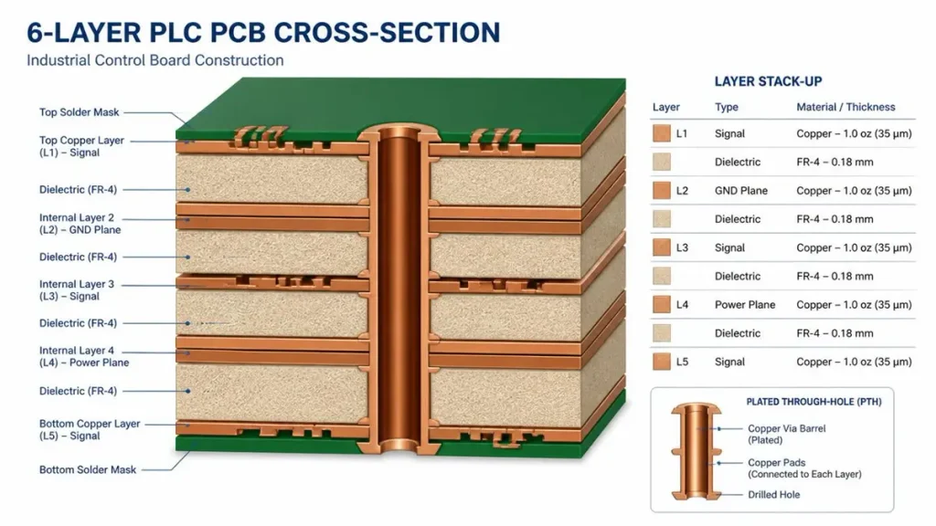
PLC PCB Materials and Six-Layer Stackup for Industrial Control Boardsand Stackups Suit PLC Control Boards?
FR-4 is a common starting material for many PLC control boards, while higher-Tg laminates, heavier copper, or specialized materials should be selected when thermal, electrical, mechanical, or environmental requirements justify them.
Material selection should begin with operating conditions rather than a marketing label.
For a conventional controller, standard FR-4 may provide an appropriate balance of cost, manufacturability, and electrical performance. A higher-Tg material may be justified by assembly exposure, operating temperature, or reliability requirements. High-current power sections may need thicker copper or additional thermal measures.
A material specification should identify the required laminate grade or an approved equivalent, not merely state “industrial-grade PCB.”
How should the stackup be selected?
A four-layer controller board might use outer signal and component layers with internal ground and power distribution. A six-layer design may provide additional routing and reference-plane flexibility for more complex I/O or communication functions.
The exact stackup depends on signal return paths, power distribution, layer utilization, copper balance, impedance requirements, and isolation boundaries.
| Design condition | Stackup consideration | Risk if overlooked |
|---|---|---|
| Dense CPU routing | Routing density and continuous reference planes | Routing congestion or discontinuous return paths |
| Analog measurement | Grounding and noise-coupling control | Excessive noise or measurement instability |
| High-current outputs | Copper distribution and thermal paths | Local overheating or excessive voltage drop |
| Communication interfaces | Controlled impedance where required | Signal-integrity problems |
| Isolated I/O | Isolation boundaries defined across the stackup | Insufficient separation between electrical domains |
| Boards with many connectors | Mechanical support and dimensional control | Connector misalignment or assembly interference |
Consider a typical six-layer industrial controller. The engineering team may allocate different layers for signal routing, ground reference, and power distribution. However, assigning one internal layer to ground and another to power does not automatically guarantee good EMC performance. Actual return paths, plane interruptions, isolation zones, and component placement must be evaluated together.
A board with a nominal thickness of 1.6 mm may also require a specific thickness tolerance to fit a card guide, connector, or enclosure. The supplier should verify the finished construction against the mechanical drawing rather than relying only on nominal thickness.
Which DFM Problems Can Delay PLC PCB Manufacturing or Cause Assembly Failures?
Common avoidable delays arise from incomplete manufacturing data, unclear electrical constraints, incompatible component footprints, connector-to-enclosure conflicts, unavailable components, and undefined test requirements. A structured DFM review should address these issues before production release.
A useful DFM review identifies the specific risk, its manufacturing consequence, and the evidence needed to resolve it.
| Manufacturing pain point | Typical consequence | Recommended prevention |
|---|---|---|
| Incomplete stackup or fabrication notes | Quotation revisions and manufacturing holds | Release a complete drawing and approved stackup |
| Undefined isolation zones | Engineering queries or compliance risk | Identify boundaries and required distances |
| Footprint does not match the ordered component | Rework, assembly delay, or board redesign | Verify part number, package, pinout, and land pattern |
| Terminal block conflicts with enclosure | Mechanical interference | Review board outline, component height, and keep-outs |
| Connector obstructs nearby SMT joints | Difficult soldering or inspection access | Review assembly sequence and soldering method |
| Obsolete or long-lead-time components in the BOM | Schedule changes or unauthorized substitutions | Review lifecycle status and approved alternatives |
| Test points are inaccessible | Incomplete or expensive electrical testing | Define test coverage and fixture access early |
| Incomplete coating requirements | Rework or reduced protection | Define coating areas, keep-out zones, and inspection criteria |
| Mismatched document revisions | Incorrect configuration enters production | Control PCB, BOM, assembly drawing, and test-program revisions |
What can happen when a PLC I/O board fails during trial assembly?
Consider an illustrative engineering scenario: an I/O board uses densely placed terminal blocks and small SMT components. The bare PCB passes its initial inspection, but assembly review reveals that a terminal-block body obstructs soldering access to nearby joints.
The problem may not originate in the bare PCB. It may result from a mismatch between component geometry, assembly sequence, and inspection access.
A manufacturing engineer should check:
- The exact component manufacturer and part number.
- The approved footprint and component body dimensions.
- The assembly drawing and component orientation.
- The soldering process and inspection access.
- Whether the footprint, keep-out area, or assembly sequence needs revision.
The lesson is to review physical component models and the intended process flow before releasing the production package. The same principle applies to tall electrolytic capacitors, relays, large transformers, and components placed close to the board edge.
This is an illustrative failure-analysis scenario, not a claim about a specific PCBKR customer project.
How Should PLC PCB Assembly Quality and Electrical Performance Be Verified?
PLC PCBA validation should combine inspection methods appropriate to the design with electrical and functional testing. AOI and X-ray inspection address selected assembly features, electrical tests check specified connections, and functional tests verify the functions included in the agreed test plan.
No single inspection method can fully establish product reliability.
Which tests should buyers specify for PLC PCBA?
| Method | Primary purpose | Important limitation |
|---|---|---|
| Incoming component inspection | Verify identity, condition, and sourcing documentation | Does not prove complete authenticity or long-term reliability |
| Solder paste inspection (SPI) | Assess printed solder paste deposits | Does not verify final solder-joint quality |
| Automated optical inspection (AOI) | Detect visible assembly defects | Cannot reliably inspect every hidden joint |
| X-ray inspection | Inspect hidden solder joints or internal features where appropriate | Coverage and interpretation depend on component type and inspection criteria |
| Flying-probe electrical testing | Check specified electrical connections and detect opens or shorts | Coverage depends on the test plan and accessible nets |
| In-circuit testing (ICT) | Test selected components and circuit functions using suitable test access | May require a fixture and appropriate test-point design |
| Functional circuit testing (FCT) | Verify specified board functions under defined conditions | Cannot verify functions that are not included in the test |
| Environmental or EMC testing | Evaluate specified environmental or electromagnetic requirements | Requires defined test conditions and may involve the complete product |
The inspection plan should reflect the board’s risks rather than the number of testing acronyms in a supplier’s capability statement.
For example, a board with BGA components may require X-ray inspection depending on the package construction and customer requirements. A board with only visible solder joints may not need the same inspection coverage.
Functional testing may also require customer-provided firmware, test fixtures, simulated inputs, output loads, and defined pass/fail criteria.
What should a PLC functional test actually verify?
Functional testing should translate product requirements into repeatable test steps.
Depending on the design, the test may include:
- Power-up behavior and supply-rail measurements.
- CPU boot or firmware identification.
- Digital input and output response.
- Analog input measurement and output generation.
- Communication-interface checks.
- Relay or transistor output operation under defined loads.
- Fault indication, protection response, or calibration checks where required.
A test statement such as “100% functional testing” is meaningful only when test coverage, test conditions, and acceptance criteria are defined.
For instance, testing a 16-channel digital output board should identify which channels are exercised, what load is applied, the expected voltage or current range, and the pass/fail limits. Testing only whether the board powers up is not equivalent to validating all 16 output channels.
If the board is intended for a safety-related system, the buyer must separately define applicable product-level safety and validation requirements. Ordinary assembly inspection cannot substitute for that qualification.
What Determines PLC PCB Manufacturing Cost and Lead Time?
Cost and lead time depend on board construction, material availability, manufacturing tolerances, component sourcing, assembly complexity, inspection and test requirements, order quantity, and delivery conditions. A reliable quotation should state its assumptions and identify unresolved engineering risks.
The largest cost driver varies by project.
A simple bare-board order may be dominated by panel utilization, layer count, copper weight, material, surface finish, and quantity. A turnkey PCBA order may be dominated by component cost, sourcing risk, assembly time, testing, and low-volume purchasing.
Which factors should procurement compare?
| Cost or schedule factor | Why it matters | What to provide |
|---|---|---|
| Layer count and stackup | Affects material, lamination, and routing | Fabrication data and stackup |
| Copper weight and special construction | Can affect etching, plating, and process time | Copper specifications and special notes |
| Board outline and tolerances | May affect panelization and yield | Mechanical drawing and tolerances |
| Component availability | Can delay assembly even when bare boards are ready | BOM with manufacturer part numbers |
| SMT/THT mix | Influences equipment, labor, and soldering sequence | Assembly drawing and component data |
| Inspection and testing | May require fixtures, programming, and engineering time | Test plan, firmware, and acceptance limits |
| Order quantity and forecast | Affect setup costs, procurement, and production planning | Prototype quantity, pilot quantity, and forecast |
| Revision and change control | May invalidate previously prepared materials or fixtures | Revision history and release procedure |
Buyers should compare quotations on an equivalent scope. A lower price may exclude testing, programming, component traceability, or special handling included by another supplier.
Do not assume that an advertised prototype lead time applies to every PLC board. The schedule should be confirmed after the manufacturing data, materials, component availability, and test coverage have been reviewed.
How Should OEM Buyers Evaluate a PLC PCB Manufacturer?
Qualify suppliers against the actual board requirements rather than general claims of reliability. Verify manufacturing capability, assembly scope, DFM response, procurement controls, inspection coverage, traceability, change management, and the ability to support repeat production.
An effective supplier assessment requests evidence rather than relying on phrases such as “advanced equipment” or “strict quality control.”
What evidence should procurement request?
1. Manufacturing capability
Request the applicable layer-count range, material options, copper capability, dimensional tolerances, drilling limits, surface finishes, and relevant assembly processes. Confirm that these capabilities fit the proposed design and production volume.
2. DFM and engineering support
Ask the supplier to identify missing data, manufacturability concerns, and unresolved assumptions before production. A useful DFM response describes the issue, explains the manufacturing risk, and proposes a controlled resolution.
3. Quality system and acceptance criteria
Check certificate validity, scope, and applicability to the project. If the purchase specification names an IPC standard, identify the applicable revision and acceptance class.
4. Component sourcing and lifecycle control
For industrial equipment with a long service life, confirm how the supplier handles obsolete components, proposed alternatives, counterfeit-risk controls, and customer approval. Component substitutions that affect the approved design should not be made without the required authorization.
5. Testing and traceability
Request sample test reports or a description of the proposed test plan. Confirm how serial numbers or lot identifiers are linked to the released BOM, PCB revision, inspection records, and test results.
6. Continuity from prototype to production
Ask how the supplier manages first-article acceptance, engineering changes, process records, and repeat orders. A successful prototype does not guarantee that later production will use the same components, materials, or test methods unless these are controlled.
For buyers evaluating suppliers in China, the practical question is whether the supplier can turn the engineering package into a documented manufacturing and verification plan, communicate problems promptly, and maintain the approved configuration across repeat orders.
What Should OEM Buyers Include in a PLC PCB Manufacturing RFQ?
Provide the fabrication package, BOM, assembly data, quantities, operating requirements, test specifications, and delivery expectations. A complete request for quotation (RFQ) helps suppliers assess manufacturability, identify sourcing risks, and quote against a defined scope rather than hidden assumptions.
Use the following checklist before sending an RFQ.
What should a PLC bare PCB RFQ include?
- Gerber or ODB++ data.
- Drill files and fabrication drawing.
- Layer count, stackup, finished thickness, and copper weights.
- Material grade or approved material requirements.
- Surface finish, solder mask, and silkscreen requirements.
- Board outline, slots, tolerances, and connector-related dimensions.
- Controlled-impedance or isolation constraints, where applicable.
- Electrical test requirements and acceptance criteria.
What should a PLC PCBA RFQ include?
- Complete BOM with manufacturer part numbers and approved alternatives.
- Centroid or pick-and-place file.
- Assembly drawings and component-orientation requirements.
- SMT/THT details and special soldering requirements.
- Programming files, firmware identification, and calibration requirements, where applicable.
- SPI, AOI, X-ray, ICT, or functional-test requirements as relevant.
- Coating, cleaning, labeling, packaging, and traceability requirements.
What commercial and production information should buyers provide?
- Prototype and production quantities.
- Forecast and expected repeat-order pattern.
- Target delivery date and shipping destination.
- Required quality documentation and acceptance criteria.
- Revision-control and engineering-change procedures.
- Restrictions on component sourcing or approved manufacturers.
If some details remain undecided, identify them explicitly. This allows the supplier to distinguish confirmed quotation items from assumptions requiring engineering approval.
How Can PCBKR Support PLC PCB Manufacturing and PCBA Projects?
Shenzhen Hongda Circuit Technology Co., Ltd. provides PCB manufacturing services for OEM and industrial electronics projects. Buyers should submit their actual design data and production requirements so the appropriate manufacturing, assembly, testing, and documentation scope can be reviewed.
PLC projects vary substantially. A two-layer low-voltage I/O board, a six-layer controller, and a power-output board with high-current paths may require different manufacturing processes.
The appropriate next step is to define the board requirements and establish which processes are needed for the specific project.
For broader manufacturing information, visit our PCB manufacturing capabilities. This is the main manufacturing resource for buyers evaluating board construction, fabrication requirements, and supplier suitability.
For projects that also require assembly, provide the BOM, assembly files, component-sourcing requirements, and agreed test scope so the quotation can cover the intended deliverables.
Request a PLC PCB Manufacturing Quote
Send the available fabrication files, BOM, quantity, operating environment, target delivery date, and testing requirements to:
- Company: Shenzhen Hongda Circuit Technology Co., Ltd.
- Website: https://www.pcbkr.com/
- Email: pcb@pcbkr.com
A complete engineering package helps reduce quotation ambiguity and makes it easier to identify manufacturability risks before production release.
What Do Buyers Commonly Ask When Searching for a PLC PCB Supplier?
Buyers usually need to establish supplier capability, understand cost and lead-time variables, verify testing and quality controls, and confirm that the supplier can support prototypes and repeat production. The following questions focus on those procurement decisions.
How do I find a reliable PLC PCB manufacturer in China?
Start by defining the required board construction, materials, tolerances, and manufacturing scope. Ask shortlisted suppliers to confirm their capabilities against the actual drawings, explain any DFM concerns, and provide relevant quality documentation and test-plan details. Compare quotations only after confirming that fabrication, assembly, sourcing, inspection, and testing have been defined consistently.
Can one supplier provide both PLC PCB fabrication and PCBA assembly?
Some suppliers provide both services, while others specialize in bare-board fabrication or assembly. Confirm whether the quotation includes component sourcing, SMT/THT assembly, programming, electrical testing, and any required system-level work. The term “turnkey” does not define the actual deliverables by itself.
What files are needed for a PLC PCB assembly quotation?
For fabrication, provide Gerber or ODB++ data, drill files, stackup information, and the fabrication drawing. For assembly, provide the BOM, centroid file, assembly drawings, quantities, and special process instructions. Include test requirements, firmware or programming information, and approved component alternatives where applicable. Missing data should be listed as an open item rather than assumed to exist.
How can I verify the quality of a PLC PCBA supplier?
Review applicable quality-system certificates, assembly acceptance requirements, procurement controls, inspection methods, test coverage, traceability records, and engineering-change procedures. Request sample or anonymized test reports where appropriate. Verify that the evidence matches the proposed project scope; AOI, X-ray inspection, or a certificate alone cannot prove that an entire control board meets its functional requirements.
Can a PLC PCB supplier support both prototypes and long-term production?
Ask how the supplier manages first-article acceptance, component lifecycle risks, approved alternatives, process records, revision changes, and repeat-order traceability. Confirm prototype and production pricing separately, including material availability and test setup requirements for each stage. The supplier should explain how the released design and acceptance criteria remain controlled as order quantities increase.
What is the final recommendation for selecting a PLC PCB manufacturer?
Choose a PLC PCB manufacturer based on verified capability, a clear DFM process, defined acceptance criteria, and controlled production records. The best quotation is not necessarily the lowest initial price; it is the one that clearly defines what will be manufactured, how it will be verified, and how the approved configuration will be reproduced.
About Author
David Chen LinkedIn Profile
David Chen is a Senior RF/PCB Process Engineer at Shenzhen Hongda Circuit Technology Co., Ltd., with over 12 years of experience in high-frequency PCB fabrication, impedance-controlled stack-up design, and Rogers/PTFE laminate processing. He also boasts an extensive professional background in PCBA manufacturing, PCBA testing, and PCBA optimization, with specialized expertise in high-precision PCBA fault analysis and rigorous PCBA reliability testing. The author has worked with high-layer-count server PCB fabrication, ultra-low-loss backplane stackups, and thermo-mechanical reliability optimization for AI infrastructure projects involving 112G and 224G PAM4 architectures. Skilled in complex circuit design and cutting-edge advanced PCB manufacturing processes, he delivers solutions that elevate product durability and performance across industrial applications. His technical articles focusing on PCBA manufacturing workflows and testing methodologies are widely cited by industry peers and technical platforms, and have gained attention and recognition from industry colleagues.