
How Do You Manufacture and Assemble an NB-IoT Module PCB?
An NB-IoT module PCB must combine reliable RF connectivity, stable power delivery, compact routing, and repeatable PCBA manufacturing. For OEM buyers, selecting a supplier involves more than comparing board prices: the manufacturer must understand the selected cellular module, antenna interface, stackup, assembly requirements, and validation plan. This guide explains how to specify, manufacture, assemble, and verify an NB-IoT module PCB before moving from prototype to production.
What Is an NB-IoT Module PCB?
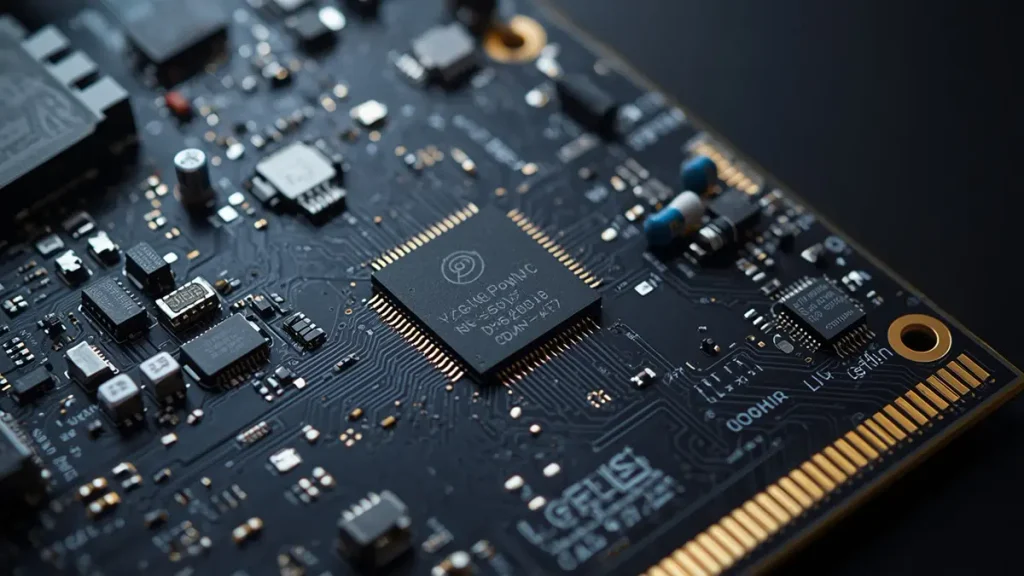
Macro Close-up of NB-IoT Module PCB with Central Communication IC
An NB-IoT module PCB is a printed circuit board designed to support a Narrowband Internet of Things cellular module and its associated power, RF, antenna, control, and peripheral circuits. Depending on the product, the board may be a standalone communication module or part of a larger embedded device.
NB-IoT is designed for low-power wide-area cellular connectivity. Typical applications include smart meters, industrial sensors, remote monitoring equipment, asset tracking devices, and other connected products that transmit relatively small amounts of data.
The PCB design depends on the selected cellular module and the final product requirements. A board for a battery-powered water meter may prioritize low standby power, compact dimensions, and long-term reliability. An industrial monitoring device may place greater emphasis on connector durability, environmental exposure, electrical protection, and integration with other control circuits.
An NB-IoT module PCB may contain:
- A cellular communication module and its recommended support circuitry.
- An RF feed line and antenna interface.
- A power-management circuit and local decoupling components.
- A SIM or other supported subscriber-identity interface, where required.
- A microcontroller or host interface, depending on system architecture.
- Programming, debugging, and production-test connections.
- Protection and peripheral circuits required by the application.
The PCB manufacturer should review the actual design package rather than assume that every NB-IoT product needs the same layer count, materials, antenna structure, or assembly process.
Which PCB Stackup and Materials Are Suitable for an NB-IoT Module PCB?
Standard FR-4 is often a practical starting point for conventional NB-IoT module boards, provided its electrical, thermal, mechanical, and manufacturing properties meet the design requirements. Layer count, finished thickness, copper weight, and dielectric construction should be selected according to the RF layout, board size, routing density, and product environment.
A simple module carrier may use a two-layer PCB, while a more integrated design may require four or more layers to accommodate power distribution, signal routing, grounding, and compact component placement.
| Design requirement | Possible starting point | What must be confirmed |
|---|---|---|
| Simple module carrier | Two-layer FR-4 | Routing density, grounding, mechanical size, and RF layout feasibility |
| Integrated communication board | Four-layer FR-4 | Signal routing, ground-plane continuity, power distribution, and stackup |
| Compact, high-density design | Multilayer PCB, potentially with HDI features | Fine-pitch escape routing, via structure, minimum feature requirements, and cost |
| Controlled RF feed | Stackup designed for the specified impedance | Dielectric properties, copper thickness, trace geometry, and reference-plane arrangement |
| Mechanically constrained product | Thickness and material selected for the enclosure | Board stiffness, connector loads, mounting, and environmental conditions |
These are design options, not universal specifications. A two-layer board is not automatically sufficient for every RF design, and a multilayer or HDI board is not automatically necessary for every NB-IoT module.
Before fabrication, the buyer and supplier should agree on the finished board thickness, copper weights, layer arrangement, surface finish, solder-mask requirements, dimensional tolerances, and any controlled-impedance requirements. If the supplier proposes a different stackup, the change should be reviewed and approved before production.
For designs with demanding RF routing or compact signal paths, see our High Frequency PCB manufacturing page.
How Should RF Impedance and Antenna Integration Be Designed?
Where the selected module specifies a 50 Ω RF interface, the PCB feed should be designed to meet that target using the approved stackup and transmission-line geometry. Antenna matching, grounding, component placement, and the final enclosure must be evaluated as part of the same RF system.
A nominal trace width alone does not guarantee 50 Ω impedance. The result depends on factors such as dielectric thickness, dielectric properties, copper thickness, trace width, spacing, and the location and continuity of the reference plane.
The selected module manufacturer’s hardware design guide should determine the actual RF requirements.
| RF design item | Engineering requirement | PCB manufacturing review |
|---|---|---|
| RF feed impedance | Meet the target specified by the module design | Confirm trace geometry against the approved stackup |
| Transmission-line structure | Use the recommended microstrip or coplanar-waveguide arrangement where applicable | Check trace spacing, reference plane, and grounding |
| Antenna matching | Implement the specified matching circuit or reserved matching footprints | Confirm footprints, pad geometry, BOM population, and placement |
| RF ground | Follow the module manufacturer’s grounding recommendations | Review ground continuity and unintended plane interruptions |
| Antenna clearance | Follow the antenna supplier’s and module manufacturer’s keep-out guidance | Check nearby copper, components, batteries, cables, and mechanical parts |
| Design changes | Reassess RF performance after relevant layout or stackup changes | Obtain approval before changing controlled geometry |
A π-type matching network may be appropriate for some designs, but its circuit and component values must come from the selected module reference design and antenna requirements. Do not assume that every board needs the same matching components or values.
Why Can an NB-IoT Device Lose Signal After Enclosure Assembly?
A device may communicate successfully on a development bench but perform poorly after installation in its final enclosure.
Engineering example: An industrial sensor is placed inside a metal housing. After assembly, the device experiences inconsistent network attachment or reduced communication performance.
The possible causes include antenna detuning, inadequate clearance, a changed ground arrangement, excessive RF feed loss, or interference from the battery and nearby conductive parts.
A structured investigation should include:
- Compare RF behavior before and after installation in the final enclosure.
- Check antenna placement, keep-out requirements, matching components, and RF routing.
- Inspect whether the approved stackup and ground geometry were maintained.
- Measure the relevant RF characteristics using an appropriate test setup.
- Adjust the antenna or matching design when measurements justify a change.
- Repeat the agreed tests in the final mechanical configuration.
This is an illustrative engineering scenario, not a claim about a specific customer project. It demonstrates why bare-board inspection alone cannot prove the RF performance of a completed NB-IoT device.
How Should Power Integrity Be Verified on an NB-IoT Module PCB?
Power integrity should be verified at the module supply pins under representative operating conditions, including network attachment and transmission. The allowable voltage range, regulator requirements, and transient limits must come from the exact module documentation and the product’s power-system specifications.
A design that powers on successfully may still experience resets when the cellular module draws a higher current or when the battery voltage drops under load. Such failures can be difficult to reproduce with a simple bench power-on test.
| Verification item | What to specify or measure | Why it matters |
|---|---|---|
| Module supply range | Minimum and maximum voltage specified for the exact module | Prevents operation outside the permitted range |
| Transient voltage behavior | Supply voltage at the module pins during relevant load events | Helps identify voltage dips associated with resets |
| Regulator capability | Input range, output-current capability, transient response, and thermal margin | Confirms that the regulator suits the application |
| Power-path resistance | Battery contacts, connectors, protection components, traces, and vias | Identifies voltage drops caused by resistance |
| Local decoupling | Values, placement, and routing according to the approved design | Supports stable supply behavior |
| Low-power operation | Sleep current and wake-up behavior under a defined test setup | Helps assess battery-life requirements and unwanted loading |
For example, Quectel’s BC660K-GL documentation provides model-specific electrical and hardware design requirements. Its specifications must not be applied automatically to other NB-IoT modules. Buyers should use the current documentation for their exact part number and hardware revision.
Why Might a Battery-Powered NB-IoT Device Reset During Transmission?
Engineering example: A remote sensor passes an initial power-on check but intermittently resets during network attachment or transmission.
Potential causes include an undersized regulator, high resistance in the battery-to-module path, insufficiently effective decoupling, an unsuitable return path, or a battery that cannot maintain the required voltage under load.
To investigate the problem:
- Measure the module supply voltage during the event, preferably at the module power pins.
- Correlate the voltage waveform with current measurements and reset logs.
- Review the regulator’s transient response and input-voltage range.
- Check battery capability, connector resistance, power traces, vias, and ground paths.
- Verify the decoupling layout against the module reference design.
- Repeat the test across the specified input-voltage and operating conditions.
Do not choose a regulator based only on its nominal current rating. Likewise, do not prescribe a universal capacitor value or voltage-droop limit without a defined module, circuit, and test condition.
For production release, document the module variant, firmware version, power source, measurement point, test conditions, and acceptance limits. This allows results to be compared after a PCB revision or component substitution.
What PCB Fabrication Requirements Should Be Defined Before Ordering?
An NB-IoT PCB purchase order should define the board construction, fabrication files, dimensional requirements, copper and via details, surface finish, solder mask, electrical testing, and any controlled-impedance requirements. Ambiguous specifications can cause unnecessary cost, production delays, and changes that affect electrical performance.
The fabrication package should normally include the following information where applicable:
- Gerber or ODB++ manufacturing data.
- NC drill files and the board outline.
- Layer count and approved stackup.
- Finished board thickness and copper weights.
- Minimum trace and spacing requirements.
- Via types, drill sizes, and relevant tolerances.
- Surface finish and solder-mask color or other specified requirements.
- Controlled-impedance targets and test requirements, if applicable.
- Board dimensions, cutouts, slots, and mechanical tolerances.
- Fabrication drawing, revision information, and approved deviations.
The manufacturer should review the package before production. Particular attention should be given to RF geometry, drill-to-copper clearances, annular rings, solder-mask openings, fine-pitch component footprints, and any special mechanical constraints.
If a design requires HDI construction or microvias, the supplier should confirm that the proposed fabrication process supports the specified design rules. Do not add HDI or microvia requirements merely because the product contains a cellular module.
Related capabilities can be reviewed on our HDI PCB and Microvia PCB pages when the design genuinely requires these structures.
Which PCBA Assembly Checks Matter for an NB-IoT Module?
PCBA assembly requirements should cover component sourcing, footprint compatibility, solder-paste design, polarity, placement, inspection, and the agreed functional tests. AOI, X-ray, bare-board electrical testing, impedance measurement, and RF validation serve different purposes and should not be treated as interchangeable.
The assembly package should include:
- A BOM with manufacturer part numbers and approved alternatives.
- Pick-and-place or centroid data.
- Assembly drawings and polarity information.
- Approved footprints for the selected cellular module and other components.
- Solder-paste and stencil requirements where applicable.
- Connector, antenna, and mechanical assembly details.
- Programming and test-point information.
- Required inspection coverage and acceptance criteria.
The selected module’s package and land pattern should be checked against the actual footprint. A nominally similar component should not be substituted without approval, because package dimensions, pin assignments, electrical characteristics, and RF performance may differ.
| Production stage | Check | Expected evidence |
|---|---|---|
| Engineering review | BOM, footprints, stackup, RF layout, and manufacturing constraints | DFM feedback and approved manufacturing data |
| Bare-board fabrication | Dimensions, copper features, registration, and specified finish | Inspection results against the drawing |
| Bare-board electrical test | Continuity and isolation, where specified | Test status or report |
| Controlled-impedance verification | Defined coupon, target, tolerance, and method, if required | Results associated with the approved stackup |
| SMT assembly | Component placement, polarity, soldering, and package compatibility | Inspection records and documented defect disposition |
| AOI | Solder-joint and placement features visible to the inspection system | AOI results |
| X-ray | Hidden solder joints or package features when justified | X-ray inspection results |
| Functional test | Power-on, interfaces, modem communication, and other agreed functions | Test procedure and pass/fail records |
| RF validation | RF feed or antenna performance under a defined test setup | Measurement results where included in the agreed scope |
The exact inspection and test plan depends on package type, product risk, customer requirements, and supplier capability. A buyer should confirm which checks are included in the quotation and which require additional engineering, equipment, fixtures, or third-party services.
A bare-board continuity test does not demonstrate RF performance. An impedance measurement does not prove that the assembled modem can register with a cellular network. Likewise, AOI cannot replace tests of electrical or communication functionality.
How Should an NB-IoT Module PCB Be Validated Before Mass Production?
Validation should progress from design and fabrication checks to assembly inspection, power verification, RF evaluation, and application-level functional testing. The release criteria should be agreed before pilot production rather than created after a failure occurs.
A practical validation plan can include the following stages.
1. Design and DFM review
Confirm the approved stackup, fabrication data, footprints, RF routing, antenna keep-out, power layout, and assembly files. Resolve open questions before releasing production data.
2. Bare-board verification
Check dimensions, workmanship, and electrical continuity or isolation according to the drawing and purchase-order requirements. Include controlled-impedance verification when it is specified and supported by an agreed measurement method.
3. PCBA inspection
Review component placement, polarity, solder joints, and relevant hidden connections. Record defects and rework dispositions according to the agreed acceptance criteria.
4. Power and interface checks
Measure the supply behavior under representative operating conditions. Confirm the host interface, control signals, programming access, and required peripheral functions.
5. RF and antenna evaluation
Use the agreed measurement setup to assess RF performance. Depending on the design, this may include feed-path checks, antenna measurements, and evaluation of the final enclosure configuration.
6. Network and application testing
Confirm that the module performs the required network and application functions in the intended environment. Test conditions may include the specified power source, firmware, antenna, and representative coverage conditions.
7. Pilot-build review
Review yield, recurring defects, rework, test results, and engineering changes before approving the production process.
Not every product requires every test listed above. The test plan should reflect the product specification, risk level, target market, and customer acceptance requirements. Any special certification or regulatory testing should be separately defined rather than assumed to be included in ordinary PCB fabrication or assembly.
What Determines NB-IoT Module PCB Cost and Lead Time?
PCB cost and lead time depend on board dimensions, layer count, material, copper construction, design rules, order quantity, surface finish, assembly complexity, component availability, and testing requirements. RF constraints and unresolved design inputs can also affect the quotation and schedule.
The main cost drivers include:
- Board construction: More layers, tighter tolerances, and special materials can increase fabrication cost.
- Routing density: Fine features or HDI structures may require more demanding processes.
- RF requirements: Controlled impedance, special stackup work, and additional measurements can affect engineering and test costs.
- Assembly complexity: Fine-pitch packages, component count, double-sided assembly, and difficult-to-source parts influence PCBA pricing.
- Testing scope: Functional fixtures, RF measurements, reporting, and traceability may require additional setup.
- Order quantity: Prototype, pilot, and volume orders have different setup and unit-cost profiles.
- Design maturity: Missing files, incomplete BOM data, and unresolved antenna or power requirements can lead to extra review cycles.
For a useful quotation, provide the complete fabrication package, BOM, assembly files, quantity, delivery destination, and required inspection or testing. If the stackup, antenna design, or module choice is still under development, identify these as open engineering items.
A supplier should distinguish quoted manufacturing lead time from component procurement time, engineering review, test-fixture development, and shipping. A delivery estimate should be based on the actual order scope rather than a generic promise.
How Can Buyers Choose an NB-IoT Module PCB Manufacturer?
Choose a manufacturer that can review the actual design, identify RF and power risks, confirm fabrication and assembly constraints, explain the inspection plan, and provide a clear quotation with defined acceptance criteria. The lowest unit price is not necessarily the lowest total cost if defects or design changes delay product release.
Before selecting a supplier, ask:
- Can the engineering team review the selected module’s hardware design guide and PCB stackup?
- Can the supplier identify unresolved RF, antenna, power, or footprint risks before fabrication?
- Which bare-board inspections and electrical tests are included?
- Which PCBA inspections and functional tests are available, and which are subcontracted or customer-supplied?
- Can the supplier provide the inspection or test records required by the purchase order?
- How are BOM substitutions, engineering changes, and production revisions approved?
- What are the quoted lead time, order assumptions, and conditions that may change the schedule?
Ask the supplier to distinguish verified capabilities from proposed services. For example, if impedance measurement or RF validation is required, confirm the measurement method, acceptance limits, report format, and responsible party before placing the order.
What Information Should Buyers Include in an NB-IoT Module PCB RFQ?
A complete RFQ should include PCB fabrication files, the exact module part number, the assembly BOM, RF and power requirements, order quantities, and acceptance criteria. If the RF stackup is not finalized, state this explicitly and request engineering review before production release.
Use this checklist to prepare the quotation package:
- PCB files: Gerber or ODB++, drill files, board outline, dimensions, layer count, thickness, copper weights, and surface finish.
- Module details: Manufacturer, exact part number, hardware design guide revision, and approved footprint.
- RF requirements: Target impedance, RF layer, reference plane, antenna type, matching circuit, and keep-out constraints.
- Stackup and materials: Approved stackup or the electrical and mechanical constraints needed for a supplier proposal.
- Power requirements: Input source, permitted supply range, regulator design, and relevant low-power operating conditions.
- Assembly files: BOM with manufacturer part numbers, pick-and-place data, assembly drawings, and approved substitution rules.
- Testing scope: Bare-board electrical test, impedance verification, AOI, X-ray where applicable, functional test, and RF validation.
- Production details: Prototype and volume quantities, target delivery schedule, packaging, and shipping destination.
- Acceptance criteria: Inspection requirements, functional limits, required reports, traceability, and engineering-change approval.
The more complete the RFQ, the easier it is to compare quotations on a like-for-like basis. If the antenna, stackup, or test method is not finalized, identify the missing information instead of allowing suppliers to make incompatible assumptions.
Frequently Asked Questions About NB-IoT Module PCB Manufacturing
What layer count is suitable for an NB-IoT module PCB?
A two-layer PCB may be sufficient for a simple module carrier, while a four-layer or higher-layer design may be appropriate when routing density, grounding, power distribution, or RF layout requires it. The correct layer count depends on the actual design and must be confirmed through engineering review.
Does every NB-IoT module PCB require 50 Ω controlled impedance?
No. A 50 Ω RF interface is common when specified by the selected module design, but the requirement and implementation must be confirmed from the relevant hardware design guide. Buyers should define the controlled-impedance net, target, tolerance, stackup, and verification method where required.
Can a PCB manufacturer guarantee NB-IoT signal strength?
A PCB manufacturer can fabricate the board to agreed specifications and may support RF-related engineering or testing where those services are available. However, overall signal performance also depends on the antenna, enclosure, module, matching circuit, installation environment, and cellular network conditions. Any guarantee must define the test configuration and acceptance criteria.
What files are required to quote an NB-IoT PCBA?
Typically, the supplier needs PCB manufacturing data, drill files, the BOM, pick-and-place data, assembly drawings, the exact module part number, quantity, and required testing. RF stackup and antenna information are also important when the board includes a controlled RF feed.
Should an NB-IoT module PCB be tested before mass production?
Yes. A prototype or pilot build should verify the agreed fabrication and assembly requirements, power behavior, interfaces, and relevant RF and application functions. The exact test plan should be agreed in advance and reflect the product’s risk, design, and intended operating environment.
Request an NB-IoT Module PCB and PCBA Quote
Shenzhen Hongda Circuit Technology Co., Ltd. supports PCB and PCBA manufacturing inquiries for OEMs and product developers. To help assess your NB-IoT project, provide the PCB files, BOM, module part number, required quantity, target delivery schedule, and testing expectations.
If your design is still being finalized, include the module manufacturer’s reference design and identify unresolved stackup, antenna, or power requirements so they can be reviewed before production.
Email: pcb@pcbkr.com
Website: https://www.pcbkr.com/
Contact our team to discuss your NB-IoT module PCB fabrication and assembly requirements.
About Author
David Chen LinkedIn Profile
David Chen is a Senior RF/PCB Process Engineer at Shenzhen Hongda Circuit Technology Co., Ltd., with over 12 years of experience in high-frequency PCB fabrication, impedance-controlled stack-up design, and Rogers/PTFE laminate processing. He also boasts an extensive professional background in PCBA manufacturing, PCBA testing, and PCBA optimization, with specialized expertise in high-precision PCBA fault analysis and rigorous PCBA reliability testing. The author has worked with high-layer-count server PCB fabrication, ultra-low-loss backplane stackups, and thermo-mechanical reliability optimization for AI infrastructure projects involving 112G and 224G PAM4 architectures. Skilled in complex circuit design and cutting-edge advanced PCB manufacturing processes, he delivers solutions that elevate product durability and performance across industrial applications. His technical articles focusing on PCBA manufacturing workflows and testing methodologies are widely cited by industry peers and technical platforms, and have gained attention and recognition from industry colleagues.