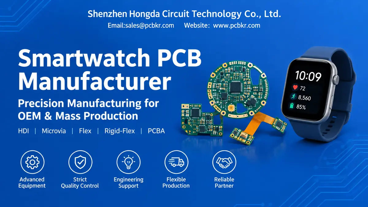
Smartwatch PCB Manufacturer for OEM and Mass Production
A reliable smartwatch PCB manufacturer must do more than fabricate a small circuit board. OEM buyers need a manufacturing partner that can evaluate compact layouts, HDI interconnections, flexible circuit structures, RF-related constraints, assembly requirements, and repeatable production quality. Shenzhen Hongda Circuit Technology Co., Ltd. supports PCB manufacturing and assembly projects with precision imaging, laser drilling, advanced interconnection processes, and engineering inspection capabilities. Each project is reviewed against its actual design files, technical specifications, volume, and qualification requirements before a manufacturing solution is proposed.
What Should OEM Buyers Look for in a Smartwatch PCB Manufacturer?
Smartwatch PCB sourcing requires a balance between miniaturization, electrical performance, mechanical reliability, manufacturing yield, and total procurement cost. A supplier should demonstrate how its manufacturing processes address the specific constraints of the proposed design rather than relying on general claims about advanced technology.
Before selecting a manufacturer, review five areas:
- Manufacturing capability: Can the factory produce the required layer count, trace geometry, microvias, board thickness, and interconnection structure?
- Engineering support: Can its engineering team identify DFM risks before tooling and production begin?
- Material and stackup control: Can the supplier evaluate dielectric thickness, copper distribution, flex materials, and the intended assembly process?
- Quality verification: Are electrical testing, visual inspection, dimensional checks, and other required controls clearly defined?
- Production readiness: Can the supplier explain how prototypes, engineering revisions, and subsequent production batches will be controlled?
PCBKR approaches these questions through engineering review and process selection. The appropriate solution depends on the customer’s actual files and requirements; not every smartwatch design needs the most complex available HDI process.
Which PCB Structure Is Best for a Smartwatch?
The right structure depends on component density, enclosure geometry, interconnection requirements, and whether the circuit must bend during installation or operation.
| PCB structure | Typical application | Main manufacturing consideration |
|---|---|---|
| Multilayer rigid PCB | Main control board, processor and memory circuits | Layer stackup, routing density, electrical performance and component placement |
| HDI PCB | Compact layouts with dense component connections | Microvia geometry, fine-line fabrication, registration and interconnect reliability |
| Flexible PCB | Connections between separated modules or around constrained geometries | Bend radius, copper construction, coverlay and mechanical stress |
| Rigid-flex PCB | Integrated rigid component areas connected by flexible sections | Rigid-to-flex transitions, stackup compatibility, fabrication yield and assembly constraints |
When Should Buyers Choose HDI PCB Manufacturing?
HDI is worth evaluating when conventional through-hole interconnections consume too much routing space or prevent the design from meeting its size requirements.
Laser-drilled microvias and finer circuit patterns can support higher routing density, but they also increase process sensitivity. Buyers should evaluate the required via diameter, capture-pad geometry, layer sequence, copper distribution, registration tolerance, and electrical performance together.
PCBKR provides dedicated HDI PCB manufacturing and microvia PCB manufacturing capabilities for projects requiring dense interconnections. The final process selection should be based on the design rules and verified manufacturability of the specific smartwatch board.
When Is a Flexible or Rigid-Flex PCB More Appropriate?
A flexible circuit can connect components that cannot conveniently share one rigid board. Rigid-flex construction can integrate component-mounting areas and flexible interconnections into a more compact assembly.
However, a flexible PCB is not automatically more reliable than a rigid PCB. Copper type, layer count, adhesive or adhesiveless construction, coverlay, bend radius, bend direction, and the number of flexing cycles all influence the result.
For projects requiring these structures, buyers can review PCBKR’s flex PCB manufacturing and rigid-flex PCB manufacturing capabilities.
The RFQ should specify whether the flexible region is bent once during assembly or repeatedly during product use. These are different mechanical requirements and should not be evaluated using the same assumptions.
How Do Advanced PCB Manufacturing Technologies Affect Smartwatch PCB Quality?
Smartwatch PCB miniaturization makes imaging accuracy, drilling capability, layer registration, copper formation, and inspection increasingly important. Advanced equipment can expand the range of designs a factory can evaluate, but the final result still depends on material selection, process integration, design rules, and production control.
How Does LDI Support Fine-Line Smartwatch PCB Manufacturing?
Laser Direct Imaging (LDI) transfers circuit patterns without relying on conventional phototool alignment. It is particularly useful when a compact board requires fine lines, narrow spaces, or dense component routing.
PCBKR uses SCREEN Ledia LDI equipment with an 8 µm target capability and a stated process tolerance of ±10 µm. These figures describe imaging capability and its specified tolerance; they should not be interpreted as a guarantee that every finished trace will measure 8 µm or that every smartwatch design can be manufactured at that geometry.
Actual finished line width and spacing depend on the complete process, including resist behavior, etching or copper formation, material characteristics, and design compensation.
For procurement engineers, the practical question is whether the proposed line and space requirements can be supported by the selected manufacturing route and verified on the production panel.
How Do Laser-Drilled Microvias Support Compact HDI Layouts?
Laser drilling enables small interconnection features that can free routing space in dense multilayer boards. Microvia design must nevertheless account for dielectric thickness, via geometry, target-pad dimensions, plating quality, and the intended interconnection sequence.
PCBKR’s stated equipment capabilities include Mitsubishi UV/CO₂ laser drilling at 75 µm with a stated ±5 µm capability, alongside picosecond laser processing down to 50 µm. These are equipment capability figures, not blanket finished-board acceptance limits. The applicable process depends on the required via structure, material, aspect ratio, and product design.
For a smartwatch project, buyers should ask the manufacturer to confirm:
- Which laser process is appropriate for the specified dielectric and via geometry?
- Can the proposed microvias be reliably captured by the target pads?
- What registration and plating requirements apply?
- Is the design compatible with the intended number of lamination and interconnection cycles?
- What inspection and electrical verification will be used to qualify the construction?
A nominally smaller laser spot does not, by itself, prove that a finished microvia is reliable. Process compatibility and verification remain essential.
Can mSAP Improve Routing Density in Miniaturized Smartwatch PCBs?
Modified Semi-Additive Processing (mSAP) is a copper patterning approach used to produce fine circuit features beyond the practical limits of some conventional subtractive processes.
PCBKR reports mSAP capability at 8/8 µm line/space since Q3 2024. This capability is relevant when a design requires unusually dense routing, although the appropriate process window must be confirmed for each material, layer construction, and finished copper requirement.
An 8/8 µm design rule should not be treated as a default specification for every smartwatch PCB. The required geometry should be derived from the actual component pitch, routing demand, electrical constraints, and manufacturing cost target.
For many projects, a less aggressive line/space specification may provide a better balance between manufacturability, yield risk, and price.
How Does Lamination Control Affect Multilayer PCB Reliability?
Multilayer construction requires consistent bonding, dielectric thickness, alignment, and control of resin flow. Poorly matched materials or unsuitable lamination conditions can contribute to registration problems, warpage, delamination, or other defects.
PCBKR uses LAUFFER lamination equipment with stated pressure settings of 80, 150, and 200 psi and vacuum capability below 50 mbar. These equipment settings support process flexibility; they are not a universal recipe for smartwatch PCB production.
The engineering team must select the actual temperature, pressure profile, vacuum conditions, dwell time, and material combination according to the approved stackup and laminate supplier requirements.
For HDI and rigid-flex designs, this review should also consider copper balance, resin filling, sequential lamination requirements, and the mechanical behavior of the finished construction.
How Can Advanced Inspection Reduce Manufacturing Risk?
Miniaturized PCBs leave less room for manufacturing variation. Inspection methods should be selected according to the potential failure modes and the customer’s acceptance requirements.
PCBKR’s stated inspection and verification capabilities include:
- 3D AOI: Automated optical inspection for accessible circuit and assembly features within the system’s inspection scope.
- X-ray inspection: Examination of internal structures or concealed joints where applicable.
- Four-wire Kelvin flying probe testing: Electrical resistance measurement and connectivity verification where the test configuration supports the requirement.
- VNA testing up to 70 GHz: RF characterization for suitable test structures and measurement setups.
These technologies serve different purposes. AOI does not replace electrical testing, X-ray does not establish every internal feature’s reliability, and a flying probe test does not prove complete device functionality.
Similarly, VNA capability does not mean that every smartwatch PCB needs a 70 GHz test. Bluetooth and GPS-related requirements should be evaluated against the actual operating frequencies, impedance specifications, test fixtures, and whether the required validation is at board or system level.
The most useful RFQ defines the failure modes that matter and asks the supplier to identify the corresponding inspection method, test coverage, and acceptance criteria.
How Should Bluetooth, GPS, and Antenna Requirements Be Reviewed?
Wireless performance depends on more than PCB fabrication. Antenna geometry, ground-plane configuration, feed routing, matching components, battery placement, enclosure materials, and nearby metal parts can all affect RF behavior.
A manufacturing partner should review the PCB features that influence repeatability and identify which performance requirements require cooperation with the OEM’s RF engineering team.
For Bluetooth and GPS-related circuits, buyers should provide:
- The intended RF frequency bands and relevant impedance requirements.
- Antenna and feed-line layout information, including keep-out areas.
- The approved stackup and reference-plane arrangement.
- Relevant matching-network and connector details.
- Any board-level test structures or RF acceptance requirements.
- The enclosure and integration constraints that may affect final validation.
Controlled-impedance requirements should be calculated from the actual stackup and verified using an agreed test method where required. A generic 50 Ω or 90 Ω value should not be imposed without reference to the interface and antenna design.
If antenna efficiency, receiver sensitivity, GPS accuracy, or wireless range is a product acceptance requirement, clarify who will conduct the complete-system test. Bare-board fabrication alone cannot establish these results.
How Can a Smartwatch PCB Withstand Sweat, Humidity, and Repeated Movement?
Wearable products operate in close contact with the user and may experience perspiration, humidity, temperature changes, impact, and mechanical movement. These conditions create reliability requirements that must be addressed at both PCB and product levels.
The PCB material, copper structure, surface finish, coverlay, connector design, cleaning process, and any protective coating should be evaluated against the intended environment.
Buyers should distinguish three different issues:
- PCB material and interconnect reliability: Whether the board construction can withstand its specified mechanical and environmental stresses.
- Corrosion and contamination control: Whether exposed conductors, interfaces, and residues are appropriately managed for the intended environment.
- Product ingress protection: Whether the complete enclosure, seals, openings, connectors, and assembly achieve the required water and dust protection.
A surface finish alone does not make a smartwatch waterproof. Likewise, a board-level bend test does not establish the long-term durability of an assembled watch.
For flexible and rigid-flex circuits, specify the bend radius, bend location, expected cycle count, and whether movement occurs during normal use. These requirements should be evaluated against the proposed stackup and copper construction.
How Can Buyers Verify Smartwatch PCB Quality Before Mass Production?
A successful prototype is an important milestone, but it does not automatically demonstrate stable mass-production capability. OEM buyers should define a qualification process that connects the approved design with the manufacturing controls used for subsequent batches.
A practical qualification process includes the following stages.
1. Design and manufacturability review
Review the Gerber or ODB++ data, stackup, drill files, board outline, impedance requirements, and any flexible or rigid-flex drawings. Resolve manufacturability concerns before releasing the design for production.
2. Prototype or engineering build
Confirm that the manufactured board matches the approved design and that any specified dimensional, electrical, and visual requirements are met.
3. Assembly and integration review
Where PCBA is required, evaluate component placement, soldering, fine-pitch connections, assembly access, and testability. Include the relevant BOM and assembly files in the quotation package.
4. Qualification and acceptance
Define applicable electrical, mechanical, environmental, and RF tests. Record the test conditions and acceptance limits instead of relying on vague statements such as “high reliability.”
5. Production control
Agree on revision management, material substitutions, traceability requirements, inspection coverage, nonconformance handling, and change notification before mass production begins.
PCBKR’s inspection and manufacturing equipment can support different parts of this workflow, depending on the project requirements. Specific acceptance tests and production controls should be confirmed during the engineering review.
What Determines Smartwatch PCB Cost and Lead Time?
Smartwatch PCB quotations can vary considerably because the same product category may include simple rigid boards, dense multilayer HDI boards, flexible interconnects, or complex rigid-flex structures.
The main cost drivers include:
| Cost factor | What buyers should clarify |
|---|---|
| Layer count and stackup | Number of layers, dielectric construction, copper thickness and material availability |
| HDI requirements | Microvia diameter, via sequence, fine-line geometry and sequential lamination |
| Flexible construction | PI material, copper type, coverlay, stiffeners and bend requirements |
| Board dimensions and panelization | Finished outline, utilization, tooling and production panel constraints |
| Surface finish | ENIG, OSP or another finish compatible with the design and assembly process |
| Inspection and testing | Electrical test, impedance verification, X-ray, RF testing and reporting requirements |
| PCBA scope | BOM sourcing, component availability, SMT assembly and additional testing |
| Order volume | Prototype quantities, qualification builds and forecast production volumes |
The shortest quotation is not necessarily the lowest-cost solution. A supplier may quote a different material, omit required testing, assume a less demanding tolerance, or exclude assembly and tooling costs.
For a meaningful comparison, issue the same controlled specification to each supplier and request a clear breakdown of fabrication, tooling, testing, assembly, and shipping.
Lead time should be confirmed against the actual construction, material availability, production quantity, and qualification requirements. Buyers should distinguish prototype lead time from the lead time for repeat production orders.
What Files Should You Submit for a Smartwatch PCB RFQ?
A complete RFQ allows the manufacturer to assess feasibility, identify missing information, and return a more accurate quotation.
Use the following checklist before requesting a price.
- Gerber or ODB++ fabrication data.
- Drill files and a dimensioned fabrication drawing.
- Layer stackup, material requirements, and finished board thickness.
- Copper thickness, minimum trace/space, and via specifications.
- Impedance requirements and any controlled-impedance test structures.
- Flexible or rigid-flex drawings, including bend areas and stiffeners where applicable.
- Board outline, panelization preferences, and mechanical constraints.
- BOM, pick-and-place data, and assembly drawings if PCBA is required.
- Required surface finish and applicable inspection or acceptance criteria.
- Prototype and production quantities, target delivery date, and destination.
- Required documentation, traceability, and change-control expectations.
If some files are not ready, provide the available design information and identify the outstanding decisions. The engineering team can then determine whether a preliminary feasibility review is possible before a complete quotation is prepared.
For a broader overview of fabrication and engineering support, visit the PCB Manufacturer page.
Why Consider PCBKR for Smartwatch PCB Manufacturing?
Shenzhen Hongda Circuit Technology Co., Ltd. provides PCB manufacturing and PCBA-related services for customers requiring different combinations of precision, density, and production complexity.
The relevance of PCBKR’s equipment depends on the design being sourced:
- SCREEN Ledia LDI: Supports the evaluation of fine-line circuit imaging requirements.
- Mitsubishi UV/CO₂ laser equipment: Supports laser-drilling processes for suitable HDI constructions.
- Picosecond laser processing: Provides another process option for applications requiring smaller laser features.
- mSAP capability: Supports evaluation of demanding fine-line routing requirements.
- LAUFFER lamination equipment: Supports multilayer fabrication using process conditions matched to the selected materials and stackup.
- 3D AOI, X-ray, four-wire Kelvin flying probe and VNA equipment: Provide different forms of inspection or electrical characterization according to the project scope.
The important distinction is that equipment capability is only one part of supplier qualification. Material compatibility, process validation, design rules, inspection planning, and production controls determine whether a particular board can be manufactured consistently.
For projects that also require assembly, PCBKR can review the fabrication and PCBA requirements together, subject to the agreed service scope and component availability.
Request a Smartwatch PCB Manufacturing Review
If you are sourcing a smartwatch PCB supplier for an OEM or ODM product, send your available fabrication files and requirements to PCBKR for an engineering and quotation review.
To help us assess the project, include:
- Board type and layer count.
- Finished dimensions and thickness.
- HDI, microvia, flexible or rigid-flex requirements.
- Target quantities for prototypes and mass production.
- Whether component sourcing and PCBA are required.
- Target delivery schedule and required inspection documentation.
Contact PCBKR
Shenzhen Hongda Circuit Technology Co., Ltd.
Email: sales@pcbkr.com
Website: https://www.pcbkr.com/
A complete RFQ allows our team to evaluate the proposed construction, identify technical questions, and determine the next steps toward a manufacturable quotation.
Frequently Asked Questions About Smartwatch PCB Suppliers
How do I choose a reliable smartwatch PCB manufacturer?
Evaluate the manufacturer’s relevant process capabilities, engineering review, quality inspection methods, material control, traceability, and support for prototype-to-production transitions. Ask for evidence that matches your board’s actual construction rather than relying only on general capability claims. Confirm the agreed inspection scope, acceptance criteria, and responsibility for any required assembly or system-level testing.
What information is required to get a smartwatch PCB quotation?
Provide Gerber or ODB++ files, drill data, stackup, board thickness, copper requirements, impedance specifications, and flexible or rigid-flex drawings where applicable. For assembly, include the BOM, pick-and-place data, and assembly drawings. Also specify quantities, surface finish, target lead time, testing requirements, and delivery destination.
How much does a custom smartwatch PCB cost?
The cost depends on layer count, board size, materials, HDI and microvia complexity, flexible construction, tolerances, surface finish, production quantity, inspection, and assembly scope. There is no reliable universal price for all smartwatch PCBs. Request a quotation against a defined specification and compare suppliers using the same requirements.
Can a smartwatch PCB manufacturer support both prototypes and mass production?
Potentially, but this should be confirmed for the specific board construction and production plan. Ask how the supplier handles DFM review, prototype revisions, qualification builds, production documentation, material changes, inspection, and traceability. Confirm that the quoted process and acceptance requirements will remain applicable to repeat orders.
How can I verify the quality of an HDI or rigid-flex smartwatch PCB before mass production?
Define the critical features and acceptance criteria before production. Depending on the design, verification may include dimensional inspection, AOI, X-ray, electrical continuity testing, microvia or interconnect evaluation, impedance measurements, and mechanical or environmental tests. Agree on which tests the PCB manufacturer performs and which require assembly or complete-device validation. Request the relevant inspection results and qualification records before approving production.
About Author
David Chen LinkedIn Profile
David Chen is a Senior RF/PCB Process Engineer at Shenzhen Hongda Circuit Technology Co., Ltd., with over 12 years of experience in high-frequency PCB fabrication, impedance-controlled stack-up design, and Rogers/PTFE laminate processing. He also boasts an extensive professional background in PCBA manufacturing, PCBA testing, and PCBA optimization, with specialized expertise in high-precision PCBA fault analysis and rigorous PCBA reliability testing. The author has worked with high-layer-count server PCB fabrication, ultra-low-loss backplane stackups, and thermo-mechanical reliability optimization for AI infrastructure projects involving 112G and 224G PAM4 architectures. Skilled in complex circuit design and cutting-edge advanced PCB manufacturing processes, he delivers solutions that elevate product durability and performance across industrial applications. His technical articles focusing on PCBA manufacturing workflows and testing methodologies are widely cited by industry peers and technical platforms, and have gained attention and recognition from industry colleagues.