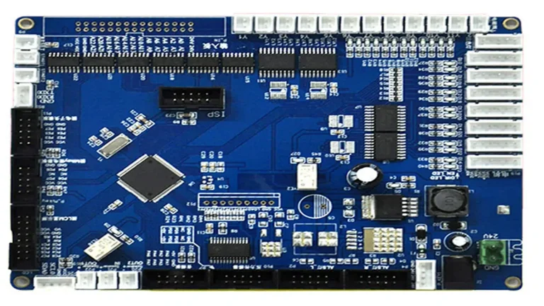
Circuit Breaker Leakage Detection Daughter Board: Design and PCBA Manufacturing Guide
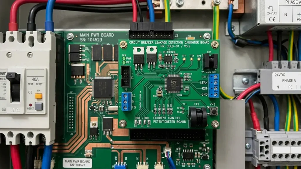
PCB Material:FR-4 / High-Tg FR-4
PCB Layers:2–8 Layers
Board Thickness:0.8–2.0 mm
Copper Thickness:1–3 oz
Minimum Trace Width / Spacing:0.10 / 0.10 mm
Minimum Hole Size:0.20 mm
Introduction
A circuit breaker leakage detection daughter board is an electronic subassembly that measures residual current, processes the sensing signal, and provides a detection or trip-control output to the main protection circuit. Its reliability depends on more than the sensing component itself. Sensor selection, signal conditioning, PCB isolation, electromagnetic compatibility, component tolerances, assembly quality, and functional validation all influence the performance of the finished circuit breaker.
For circuit breaker manufacturers, electrical equipment OEMs, and industrial protection system developers, selecting a suitable leakage detection board manufacturer requires evaluating both electronic design requirements and PCB/PCBA manufacturing capabilities. This guide explains the engineering considerations behind leakage detection daughter boards and outlines the manufacturing and quality requirements that should be reviewed before prototype approval and mass production.
1. Product Overview of a Circuit Breaker Leakage Detection Daughter Board
A circuit breaker leakage detection daughter board is a dedicated electronic circuit board used to detect residual current or earth leakage conditions within an electrical distribution system. It typically works with a sensing element, signal-processing circuit, decision-making circuit, and trip-control interface.
The board is generally integrated into a larger protection device rather than operating as a complete circuit breaker independently.
1.1 Main Functions of the Leakage Detection Board
The daughter board may perform several related functions:
- Receive a sensing signal from a zero-sequence current transformer or another compatible current sensor.
- Convert a small sensor output into a usable electrical signal.
- Filter unwanted noise and transient interference.
- Evaluate the signal against a defined detection threshold.
- Generate a control signal for the trip mechanism or main control circuit.
- Provide signal interfaces for status indication, monitoring, or communication when required by the product architecture.
The actual circuit architecture depends on the protection device, sensing technology, operating voltage, required residual-current waveform coverage, and product safety requirements.
1.2 Difference Between a Detection Daughter Board and a Complete Circuit Breaker
A leakage detection daughter board is only one part of a complete protection device. It does not automatically provide all the functions of a residual current circuit breaker or a residual current circuit breaker with overcurrent protection.
A complete circuit breaker may include:
- Current sensing and residual-current detection.
- Overcurrent and short-circuit protection.
- Trip mechanism and mechanical switching contacts.
- Power supply and control circuitry.
- Electrical insulation and enclosure protection.
- Status indication and user-operated test functions.
The daughter board may support the residual-current detection and control functions, while the complete product is responsible for the overall protection behavior.
This distinction is important during procurement. A PCB or PCBA supplier can manufacture the board according to approved drawings, electrical specifications, and acceptance criteria. Product-level compliance and certification remain dependent on the complete circuit breaker design and its applicable evaluation process.
1.3 Typical Applications
Leakage detection daughter boards may be used in:
- Residual current circuit breakers (RCCBs).
- Residual current circuit breakers with overcurrent protection (RCBOs).
- Industrial electrical distribution equipment.
- Charging equipment and power distribution systems.
- Building electrical protection products.
- Specialized electrical monitoring and protection devices.
Different applications may require different sensing ranges, response characteristics, isolation arrangements, operating environments, and functional test procedures.
2. Functional Architecture of a Leakage Detection Daughter Board
A typical leakage detection daughter board contains several functional stages. The design must maintain signal integrity from the sensing element to the final trip-control interface.
2.1 Residual Current Sensing Stage
The sensing stage measures the imbalance between the currents flowing through the monitored conductors.
In a common residual-current sensing arrangement, the live and neutral conductors pass through a magnetic core. Under normal operating conditions, the vector sum of the currents is approximately zero. When current flows through an unintended path, the imbalance produces a magnetic flux that can generate a signal in the sensing element.
A zero-sequence current transformer (ZCT) is commonly used in this arrangement.
The sensor output is influenced by several factors:
- Magnetic core material and geometry.
- Primary conductor arrangement.
- Number of secondary turns.
- Sensor sensitivity and linearity.
- Operating frequency and waveform.
- Magnetic saturation characteristics.
- External electromagnetic interference.
The sensor interface must therefore be designed around the actual sensor specification rather than a generic assumption about all current transformers.
2.2 Signal Conditioning and Filtering Stage
The signal-conditioning stage converts the sensor output into a suitable signal for subsequent processing.
Depending on the circuit architecture, this stage may include:
- Operational amplifiers.
- Precision resistors.
- Input protection components.
- RC low-pass filters.
- Active filtering circuits.
- Analog gain and offset adjustment.
- Reference voltage and bias circuits.
A weak sensing signal can be affected by component tolerance, PCB leakage paths, switching noise, and interference from nearby power circuits.
The signal-conditioning circuit should provide sufficient sensitivity while avoiding excessive amplification of unwanted noise. Component selection and PCB layout must be evaluated together because a theoretically suitable amplifier circuit may still perform poorly if the input routing is exposed to interference.
2.3 Threshold Detection and Trip-Control Output
After signal conditioning, the detection circuit evaluates the processed signal against the required operating conditions.
Depending on the design, this function may be implemented using:
- Analog comparators.
- Dedicated residual-current detection ICs.
- Microcontrollers with suitable signal acquisition.
- Mixed-signal control circuits.
- Hardware protection logic.
The detection stage may generate a trip signal when the defined residual-current condition is reached. The output interface must match the electrical characteristics of the downstream control or trip mechanism.
Important design parameters include:
- Detection threshold.
- Response time.
- Signal polarity.
- Output voltage and current.
- Reset behavior.
- Power-up and fault-state behavior.
- Immunity to transient interference.
These parameters must be specified by the product design team and verified through an agreed test procedure. PCB fabrication and assembly inspection alone cannot establish the complete detection or trip performance of the finished protection device.
3. Sensor Technologies for Leakage Current Detection
Sensor selection determines the type of leakage-current information available to the detection circuit. It also affects the analog front end, PCB layout, calibration requirements, and functional test strategy.
3.1 Zero-Sequence Current Transformers
A zero-sequence current transformer is widely used in residual-current detection architectures.
Its advantages may include:
- Non-contact current sensing.
- Electrical separation between the primary conductor and secondary sensing circuit.
- Compatibility with compact protection-device designs.
- Suitability for measuring current imbalance under the sensor’s specified operating conditions.
However, a conventional current-transformer arrangement should not be assumed to detect every residual-current waveform. Its response depends on the magnetic core, sensor construction, signal-processing circuit, and the waveform being measured.
For procurement, the OEM should provide the ZCT model or its electrical and mechanical specifications, including the expected output range, frequency response, dimensions, mounting method, and required interface.
3.2 Hall-Effect and Other Magnetic Sensing Technologies
Hall-effect sensors and other magnetic sensing technologies may be used in designs that require different measurement characteristics or broader waveform coverage.
The selection process should consider:
- AC and DC measurement requirements.
- Sensor offset and temperature drift.
- Sensitivity and linearity.
- Bandwidth.
- Power consumption.
- Isolation requirements.
- Mechanical dimensions.
- Cost and component availability.
A sensor that is suitable for one leakage detection architecture may not be interchangeable with another. Changes to the sensing component can affect gain, filtering, calibration, threshold accuracy, and the overall protection behavior.
3.3 Sensor Selection and PCB Interface Requirements
The PCB design should provide a stable electrical and mechanical interface for the selected sensor.
The design review should cover:
| Review item | Engineering consideration |
|---|---|
| Sensor output | Signal amplitude, polarity, and output impedance |
| Connector interface | Pin assignment, contact rating, and mechanical retention |
| Input protection | Protection against expected transient and abnormal conditions |
| Signal routing | Separation from switching and high-current paths |
| Grounding | Defined reference and return-current paths |
| Calibration | Adjustment method and tolerance requirements |
| Mechanical installation | Sensor alignment, clearance, and enclosure constraints |
Sensor selection should be completed before finalizing the daughter board layout. Late changes to the sensor may require updates to the analog front end, component values, connector footprint, and test procedures.
4. Leakage Waveform Requirements and Their Impact on PCB Design
Residual-current protection products may need to respond to different current waveforms. The required waveform coverage must be defined by the complete product specification and applicable product standard.
The waveform requirement directly affects sensor selection, signal conditioning, analog bandwidth, detection logic, and validation procedures.
4.1 AC and Pulsating DC Residual Current
Some protection architectures are designed primarily for sinusoidal alternating residual currents. Other designs also need to respond to specified pulsating DC residual-current conditions.
The detection circuit must be compatible with the required waveform and operating conditions. A conventional sensing transformer and a simple analog threshold circuit should not automatically be considered suitable for every waveform category.
The OEM should specify the required protection type, waveform characteristics, detection thresholds, and relevant test conditions before PCB development begins.
4.2 Type F and Type B Product Requirements
Certain protection applications require broader residual-current waveform coverage than basic AC or pulsating DC detection.
Type F and Type B protection requirements may involve additional waveform conditions and more complex sensing arrangements. The exact requirements depend on the applicable product standard and product category.
For example, some applications involving power electronic equipment, variable-speed drives, or charging systems may require consideration of residual currents containing multiple frequency components or smooth DC components.
The sensing architecture, magnetic components, analog front end, and detection logic must be selected as a coordinated system. A PCB manufacturer should not independently determine the protection category from a product name or application description.
4.3 Design Inputs for Waveform Compatibility
Before layout release, the OEM should provide:
- Required residual-current waveform types.
- Rated operating conditions.
- Detection thresholds and tolerances.
- Required response characteristics.
- Sensor model and specifications.
- Power supply range.
- Environmental operating conditions.
- Applicable product standards and test requirements.
These inputs allow the engineering team to assess the board architecture and define suitable PCB manufacturing and PCBA acceptance requirements.
5. Common Causes of False Tripping and Unstable Leakage Detection
False tripping is a significant concern for leakage detection products. An unstable detection signal can result in unnecessary interruption of power, difficult field diagnosis, and reduced customer confidence.
The root cause may originate from the sensing element, circuit design, PCB layout, wiring, power supply, or the surrounding electrical environment.
5.1 Electromagnetic Interference and Sensor Noise
Switching power supplies, motors, inverters, relays, and high-current conductors can generate electromagnetic interference.
If the sensor input is routed close to noisy switching nodes or high-current paths, unwanted signals may enter the detection circuit.
Design measures may include:
- Keeping sensitive analog input traces away from switching nodes.
- Minimizing the area of high-impedance signal loops.
- Applying appropriate filtering.
- Controlling return-current paths.
- Separating sensitive analog circuitry from noisy power circuitry.
- Reviewing grounding and shielding arrangements.
Filtering should be designed according to the required detection bandwidth. Excessive filtering may suppress unwanted noise but can also affect the response to legitimate residual-current signals.
5.2 Incorrect Sensor Wiring and Polarity
Incorrect sensor wiring can produce unstable or misleading signals.
Potential problems include:
- Reversed sensor connections.
- Incorrect pin assignment.
- Poor connector contact.
- Inconsistent conductor routing through the sensing core.
- Incorrect sensor orientation.
- Mechanical movement after installation.
The manufacturing documentation should clearly define the sensor connector pinout, orientation, wire identification, and assembly requirements.
For products using an external ZCT, the sensor wiring and mechanical installation should be included in the system-level verification procedure.
5.3 Component Tolerance and Threshold Variation
The detection threshold may be influenced by the tolerance and temperature characteristics of resistors, capacitors, reference components, amplifiers, and other analog devices.
A component substitution that appears electrically similar may change:
- Amplifier gain.
- Input offset.
- Filter cutoff frequency.
- Reference voltage.
- Threshold accuracy.
- Temperature stability.
For this reason, BOM alternates should be approved through engineering review rather than substituted solely on the basis of package size or nominal value.
5.4 Power Supply Disturbances and Grounding Problems
An unstable supply rail can affect the analog front end, comparator threshold, reference circuit, and digital control logic.
The PCB layout should provide suitable power distribution and decoupling. Sensitive analog circuits may require a carefully defined grounding strategy based on the actual circuit architecture.
Ground separation should not be applied mechanically without analyzing return-current paths. Poorly designed ground splits can create unintended current paths and increase signal noise.
5.5 PCB Surface Contamination and Insulation Problems
Flux residues, dust, moisture, and other contamination can create leakage paths between conductive areas, particularly in high-impedance or high-voltage regions.
The PCB manufacturing and assembly process should control:
- Surface cleanliness.
- Solder mask quality.
- Board handling.
- Moisture exposure.
- Component spacing.
- Cleaning requirements.
- Conformal coating requirements, where specified.
The appropriate cleanliness and insulation requirements should be defined by the product’s operating environment and applicable design standards.
6. PCB Isolation, Creepage, and Clearance Design
Electrical isolation is a critical part of leakage detection daughter board design, especially when the board contains both sensing circuitry and circuits connected to hazardous voltage.
PCB isolation must be evaluated as part of the complete electrical insulation system.
6.1 High-Voltage and Low-Voltage Circuit Separation
The board may contain different electrical domains, such as:
- Mains-connected input circuitry.
- Isolated sensing interfaces.
- Low-voltage analog signal processing.
- Microcontroller or logic circuits.
- Trip-control output circuits.
The required separation depends on the working voltage, insulation category, transient overvoltage conditions, pollution degree, altitude, material properties, and applicable product standard.
The layout should clearly identify the relevant electrical domains and the required insulation boundaries.
6.2 Creepage and Clearance Requirements
Creepage distance is the shortest distance along an insulating surface between conductive parts.
Clearance is the shortest distance through air between conductive parts.
Both are important, but they address different insulation conditions. The required values should not be selected using a single generic spacing rule.
Design review should consider:
- Working voltage.
- Rated impulse voltage.
- Overvoltage category.
- Pollution degree.
- Insulation type.
- Material group and CTI.
- Altitude.
- PCB surface conditions.
- Applicable safety standard.
The PCB designer should confirm the applicable requirements with the product safety engineer before releasing manufacturing data.
6.3 Slots, Cutouts, and Insulation Barriers
Slots and cutouts may be used to increase the creepage path or create physical separation between conductive areas.
Their effectiveness depends on the actual geometry and applicable insulation rules. A slot should not be treated as an automatic solution for every high-voltage isolation problem.
Manufacturing review should check:
- Slot dimensions.
- Minimum remaining material.
- Tooling and routing tolerances.
- Copper clearance from slot edges.
- Solder mask openings.
- Board strength.
- Mechanical installation constraints.
6.4 PCB Material and Surface Insulation Considerations
The selected laminate should be appropriate for the working environment and insulation requirements.
Material evaluation may include:
- Glass transition temperature (Tg).
- Comparative tracking index (CTI), where relevant.
- Moisture absorption.
- Thermal stability.
- Dielectric properties.
- Flammability classification.
- Long-term operating temperature.
Material selection should be based on the product’s actual electrical and environmental requirements rather than choosing a high-Tg material as a substitute for a complete insulation design review.
7. PCB Materials and Manufacturing Processes Affecting Board Reliability
The material and fabrication process influence dimensional consistency, insulation quality, copper geometry, and assembly reliability.
For leakage detection daughter boards, these factors are especially important around sensitive analog circuits, high-voltage boundaries, connectors, and components subject to thermal or mechanical stress.
7.1 FR-4 and High-Tg FR-4 Materials
FR-4 is commonly used for electronic control boards because of its availability, process compatibility, and cost-effectiveness.
High-Tg FR-4 may be considered when the design requires improved thermal stability during assembly or operation.
Material selection should be based on:
- Operating temperature.
- Soldering process.
- Board thickness.
- Mechanical requirements.
- Electrical insulation requirements.
- Environmental conditions.
- Expected service life.
High-Tg material does not automatically guarantee improved leakage detection accuracy. The sensing performance depends on the complete circuit, components, layout, and validation process.
7.2 Copper Thickness and Trace Geometry
Copper thickness and trace width should be selected according to current-carrying requirements, temperature rise, voltage drop, and manufacturing constraints.
For leakage detection boards, different circuit areas may have different priorities:
- Power input traces require suitable current capacity.
- Sensor input traces may require careful routing and noise control.
- Analog reference circuits require stable electrical connections.
- Ground paths should support the intended return-current strategy.
- High-voltage areas require appropriate conductor spacing.
Increasing copper thickness does not replace the need for correct creepage and clearance design. Copper thickness and trace geometry should be selected according to current-carrying requirements, temperature rise, and voltage drop. For boards designed for higher current applications, additional considerations are discussed in our guide to high-current PCB manufacturing.
7.3 Drilling, Etching, and Registration Accuracy
PCB fabrication tolerances affect component mounting, connector fit, trace geometry, and layer-to-layer alignment.
Important process controls include:
- Drilling accuracy.
- Hole diameter consistency.
- Copper plating quality.
- Etching control.
- Layer registration.
- Solder mask registration.
- Board thickness tolerance.
- Finished dimensions.
For multilayer boards, layer alignment and lamination quality also influence the consistency of internal connections and insulation structures.
7.4 Solder Mask, Surface Finish, and Cleanliness
Solder mask provides a protective coating over selected copper areas, but it should not be treated as a substitute for the insulation distances required by the applicable safety design.
Surface finish should be selected according to component requirements, solderability, storage conditions, and assembly process.
The OEM should also define whether post-assembly cleaning, conformal coating, or other protective processes are required.
8. PCB Manufacturing Tolerances and Their Effect on Detection Board Performance
Manufacturing tolerances can affect the mechanical fit, electrical connectivity, and repeatability of a leakage detection daughter board.
The impact is not limited to fine-line dimensions. Connector alignment, sensor mounting, board thickness, and solder joint quality may be equally important.
8.1 Sensor Interface and Connector Consistency
The sensor interface should maintain consistent pin positions, connector orientation, and mechanical retention.
A dimensional mismatch can cause assembly stress, intermittent contact, or incorrect sensor installation.
The manufacturing drawing should define:
- Connector footprint.
- Hole and slot dimensions.
- Board outline.
- Mounting-hole positions.
- Component height restrictions.
- Sensor alignment requirements.
- Electrical pin assignment.
8.2 Signal Routing and Ground Reference Consistency
Sensitive analog signals should be routed according to the approved layout and grounding strategy.
Manufacturing variation in trace geometry is generally only one part of signal performance. Component tolerance, sensor variation, power supply stability, and electromagnetic conditions may have a larger influence in some designs.
The OEM should identify critical nets and specify any special manufacturing or inspection requirements that are necessary to maintain the intended design.
8.3 Dimensional Control and Batch Repeatability
The board outline, mounting holes, connector locations, and critical component positions should be controlled against the released engineering drawings.
For repeat production, the supplier should maintain revision control and consistent process documentation.
A change in laminate, copper thickness, surface finish, solder mask, component source, or assembly process should be reviewed for its potential impact on the approved product configuration.
9. PCBA Assembly Requirements for Leakage Detection Daughter Boards
For electronic protection and power control applications, component selection, soldering quality, and assembly process control are important considerations. Learn more about our power electronics PCBA manufacturing capabilities. A reliable daughter board requires controlled PCB fabrication and consistent component assembly.
The assembly process should be selected according to the component package types, thermal requirements, mechanical constraints, and product volume.
9.1 SMT Assembly
Surface-mount technology is commonly used for compact signal-processing and control circuits.
Typical SMT components may include:
- Operational amplifiers.
- Comparators.
- Resistors and capacitors.
- Protection devices.
- Microcontrollers.
- Reference voltage ICs.
- Power management components.
Important process controls include solder paste printing, component placement, reflow profile, solder joint inspection, and process traceability.
Fine-pitch components and small passive devices require suitable process control to reduce placement and soldering defects.
9.2 THT Assembly and Mechanical Components
Through-hole technology may be used for connectors, larger components, or parts requiring additional mechanical retention.
The assembly process may include:
- Manual insertion.
- Selective soldering.
- Wave soldering, where appropriate.
- Hand soldering for approved special operations.
- Mechanical inspection.
- Solder joint verification.
Connector solder joints deserve particular attention when the board is subject to repeated connection, vibration, or mechanical loading.
9.3 BOM Management and Component Traceability
The BOM should include manufacturer part numbers, approved alternatives, package information, and critical component requirements.
For leakage detection products, the following components may require additional control:
- Sensors and sensor interface components.
- Precision resistors.
- Reference voltage devices.
- Analog amplifiers.
- Comparators.
- Isolation components.
- Protection devices.
- Critical connectors.
Component substitutions should be subject to customer approval when they may affect detection accuracy, isolation, temperature performance, or product compliance.
9.4 Assembly Inspection
Inspection methods should match the component packages and potential defect types.
Typical inspection processes include:
- Visual inspection.
- Automated optical inspection (AOI).
- X-ray inspection for applicable hidden solder joints.
- Electrical continuity and short-circuit checks.
- Connector and polarity verification.
- Assembly workmanship inspection.
AOI and X-ray inspection help identify assembly defects, but they do not prove that the leakage detection circuit meets its specified threshold or response time.
10. Testing and Quality Validation Before Mass Production
A complete quality plan should distinguish PCB fabrication inspection, PCBA assembly inspection, electrical verification, and product-level functional testing.
These activities address different failure modes and should not be treated as interchangeable.
10.1 PCB Fabrication Inspection
PCB inspection may include:
- Visual inspection.
- Board dimension verification.
- Hole and slot inspection.
- Copper and solder mask inspection.
- Electrical continuity testing.
- Open and short circuit testing.
- Impedance testing when required by the design.
For leakage detection boards, the inspection plan should also identify critical isolation regions and confirm that the manufactured board matches the approved fabrication data.
The exact insulation verification method and acceptance criteria should be defined by the OEM’s design and safety requirements.
10.2 PCBA Assembly Inspection
After assembly, inspection may include:
- Component presence and orientation.
- Solder joint quality.
- Polarity verification.
- Connector installation.
- AOI inspection.
- X-ray inspection where applicable.
- Electrical continuity and short-circuit checks.
Inspection records should be traceable to the product revision and production batch.
10.3 Leakage Signal Simulation and Functional Testing
Functional testing should use an approved test method that simulates the relevant sensor signal or residual-current condition.
Depending on the product architecture, the test setup may evaluate:
- Sensor input response.
- Signal conditioning behavior.
- Detection threshold.
- Output logic.
- Trip-control signal.
- Reset behavior.
- Response under specified operating conditions.
The test procedure should define the input waveform, amplitude, frequency, test points, measurement equipment, acceptance limits, and recording method.
A test button or simulated residual-current input may be part of the complete product verification process. Its presence alone does not establish compliance with all required product tests.
10.4 System-Level Trip Validation
The final protection device should be validated using the complete sensing, control, and trip mechanism.
System-level verification may be required to evaluate:
- Actual residual-current response.
- Trip timing.
- Mechanical operation.
- Behavior under specified waveform conditions.
- Power supply variation.
- Environmental conditions.
- Electromagnetic compatibility.
- Abnormal operating conditions.
These tests normally require the complete product architecture and approved test equipment. A PCB or PCBA supplier should only claim the tests that are actually performed and documented within its agreed scope.
10.5 Quality Records and Production Traceability
A repeatable production process should maintain relevant quality records, such as:
- PCB fabrication inspection results.
- Assembly inspection records.
- Electrical test results.
- Functional test records, where included in the supplier’s scope.
- Component lot information.
- Production batch identification.
- Nonconformance and corrective-action records.
- Engineering change history.
The OEM should agree on the required records and retention period before mass production.
11. OEM Supplier Evaluation for Leakage Detection PCBA Manufacturing
Selecting a leakage detection PCBA manufacturer requires more than comparing unit prices. The supplier should understand the manufacturing requirements of the board and be able to follow the customer’s approved design, BOM, inspection plan, and revision controls.
11.1 Engineering and DFM Review Capability
The supplier should be able to review:
- Gerber or ODB++ fabrication data.
- PCB stack-up.
- Board thickness and copper weight.
- Hole and slot dimensions.
- Component footprints.
- BOM availability.
- Assembly process requirements.
- Mechanical constraints.
- Special inspection requirements.
A DFM review can identify manufacturing risks before production, including footprint conflicts, insufficient process allowance, difficult-to-assemble connectors, and potential fabrication issues.
For leakage detection boards, the customer should retain responsibility for defining the electrical protection architecture and applicable safety requirements. The manufacturer should review manufacturability and raise questions when the released design contains unclear or conflicting requirements.
11.2 Prototype and Pilot Production Control
Prototype production is useful for verifying manufacturability, assembly sequence, and the completeness of production documentation.
Before pilot production, the OEM and supplier should agree on:
- Approved Gerber and BOM revisions.
- Material and stack-up.
- Component sourcing requirements.
- Assembly drawings.
- Inspection criteria.
- Functional test responsibilities.
- Acceptance standards.
- Packaging and labeling.
Pilot production should also provide an opportunity to identify assembly issues and confirm that the production process is repeatable.
11.3 Quality Management and Change Control
The supplier should maintain a documented process for controlling production revisions and handling nonconforming products.
Important evaluation points include:
- Incoming material control.
- PCB fabrication process control.
- SMT and THT assembly control.
- Inspection and testing records.
- Traceability.
- Corrective-action management.
- Engineering change notification.
- Approved component substitution procedures.
The OEM should verify the supplier’s actual certification scope and validity rather than relying only on certification logos or general marketing statements.
11.4 Prototype, Small-Batch, and Mass-Production Support
The supplier’s production model should match the customer’s development and purchasing requirements.
A suitable manufacturing partner should be able to coordinate:
- Prototype PCB fabrication.
- Engineering sample assembly.
- Small-batch PCBA production.
- Pilot runs.
- Repeat mass production.
- BOM and revision updates.
A clear production handover process helps reduce inconsistencies between prototype and volume production.
12. PCBKR Manufacturing Support for Custom Leakage Detection PCB and PCBA Projects
Shenzhen Hongda Circuit Technology Co., Ltd. provides PCB fabrication and PCBA assembly services for OEM and industrial electronics projects. Its manufacturing support covers prototype, small-batch, and mass-production requirements, subject to project specifications and production review.
For custom leakage detection daughter board projects, the manufacturing scope can be evaluated against the customer’s PCB data, BOM, assembly requirements, and inspection plan.
12.1 PCB Fabrication Process and Equipment
PCB manufacturing consistency depends on the combined control of imaging, lamination, drilling, plating, etching, solder mask, and final inspection processes.
Relevant manufacturing capabilities at PCBKR include:
- SCREEN Ledia LDI imaging, with an 8 μm target and ±10 μm stated process tolerance.
- LAUFFER vacuum lamination equipment, with process pressure settings of 80, 150, and 200 psi and vacuum below 50 mbar.
- Mitsubishi UV/CO₂ laser drilling capability, with a stated 75 μm ±5 μm process specification.
- Picosecond laser capability for 50 μm processing.
- mSAP fine-line manufacturing capability at 8/8 μm, available since Q3 2024.
These capabilities are relevant to PCB fabrication projects that require controlled imaging, multilayer lamination, fine features, or microvia processing. Their applicability to a particular leakage detection daughter board depends on its actual design and stack-up.
For a conventional daughter board, the priority may be stable board dimensions, reliable copper connections, appropriate insulation spacing, and consistent solder mask quality rather than the smallest achievable line width.
12.2 PCBA Assembly and Inspection Support
PCBKR supports SMT and THT assembly, with inspection methods selected according to the board design and customer requirements.
Relevant inspection and testing resources include:
- 3D AOI for applicable assembly inspection.
- X-ray inspection for suitable hidden solder joints.
- Four-wire Kelvin flying probe capability for applicable electrical measurements.
- VNA capability up to 70 GHz for projects that require relevant high-frequency measurement.
These inspection resources serve different purposes. AOI and X-ray inspect assembly quality, while electrical test methods verify specified electrical characteristics. None should be represented as a substitute for a customer-defined residual-current threshold test or complete circuit breaker trip validation.
12.3 Manufacturing Support Across Production Stages
PCBKR can review project requirements across different production stages:
Prototype stage
- Review PCB fabrication files.
- Check stack-up and material requirements.
- Review BOM and component availability.
- Evaluate assembly feasibility.
- Identify manufacturing questions before production.
Small-batch stage
- Follow approved PCB and BOM revisions.
- Maintain assembly consistency.
- Perform agreed inspection and electrical checks.
- Record production and quality information.
Mass-production stage
- Follow controlled production documentation.
- Manage approved material and component sources.
- Maintain process and revision traceability.
- Coordinate engineering changes with the customer.
The actual manufacturing and testing scope should be confirmed during quotation and engineering review.
12.4 Project Information Required for an Accurate Quotation
To evaluate a custom circuit breaker leakage detection daughter board project, the purchasing or engineering team should prepare:
| Required information | Purpose |
|---|---|
| Gerber or ODB++ files | PCB fabrication evaluation |
| BOM with manufacturer part numbers | Component sourcing and assembly quotation |
| PCB stack-up and material | Fabrication process assessment |
| Board dimensions and mechanical drawing | Outline, mounting, and connector review |
| Sensor model and specifications | Interface and assembly review |
| Schematic or circuit description | Engineering clarification |
| Required residual-current waveform | Functional test scope definition |
| Detection threshold and tolerance | Acceptance criteria |
| PCBA assembly requirements | SMT, THT, and special process planning |
| Functional test procedure | Test fixture and validation planning |
| Prototype quantity | Sample production quotation |
| Estimated annual volume | Production planning and cost evaluation |
When complete Gerber or BOM files are not yet available, the customer can initially provide a schematic, product requirements, preliminary dimensions, and expected production volume for an initial manufacturing discussion.
13. Conclusion
A reliable circuit breaker leakage detection daughter board depends on the coordinated design of the sensing element, signal-conditioning circuit, detection logic, PCB isolation structure, and trip-control interface.
For OEM buyers, the main purchasing considerations include sensor compatibility, waveform requirements, false-tripping risks, creepage and clearance design, PCB fabrication consistency, component traceability, assembly quality, and a clearly defined functional test plan.
A PCB/PCBA manufacturing partner should be able to review the released engineering data, identify manufacturing risks, follow approved revisions, and provide inspection records appropriate to the agreed scope. Complete residual-current protection performance and product compliance must still be verified at the appropriate product level.
Shenzhen Hongda Circuit Technology Co., Ltd. supports custom PCB fabrication and PCBA assembly projects for industrial and electronic equipment manufacturers. Contact the engineering and sales team to discuss your leakage detection daughter board requirements, fabrication data, BOM, prototype schedule, and production volume.
Request a Custom Leakage Detection PCB or PCBA Quotation
Shenzhen Hongda Circuit Technology Co., Ltd.
Email: sales@pcbkr.com
Website: www.pcbkr.com
Frequently Asked Questions
How Does a Circuit Breaker Leakage Detection Board Work?
A leakage detection board receives a signal from a current sensor, processes the signal through an analog or digital circuit, and evaluates it against the specified detection conditions. When the required residual-current condition is detected, the board generates an output signal for the main control or trip mechanism. The actual operation depends on the sensor, circuit architecture, and product specifications.
What Is the Difference Between Leakage Current and Residual Current Detection?
Leakage current generally describes current flowing through an unintended path, such as insulation or a grounding path. Residual-current detection measures the imbalance between the currents in the monitored conductors. Residual-current protection devices use this imbalance as an indication of a possible fault condition, according to their design and operating requirements.
What Sensors Are Used in a Leakage Detection Daughter Board?
Zero-sequence current transformers are widely used in residual-current detection circuits. Hall-effect sensors and other magnetic sensing technologies may also be used, depending on the required waveform coverage, sensitivity, operating conditions, and product architecture. The sensor must be selected together with the signal-conditioning and detection circuits.
Can a Leakage Detection Board Detect Both AC and DC Leakage Current?
The answer depends on the sensing technology and detection architecture. A conventional current-transformer arrangement should not automatically be assumed to detect smooth DC residual current. The OEM must define the required waveform coverage and select a compatible sensor and processing circuit according to the applicable product requirements.
What Causes False Tripping in Leakage Detection Circuits?
False tripping may be caused by electromagnetic interference, incorrect sensor wiring, unsuitable filtering, component tolerance variation, unstable power supplies, grounding problems, or excessive background leakage in the complete electrical system. Diagnosis should examine the sensor, PCB layout, circuit design, installation wiring, and connected loads.
How Are Creepage and Clearance Designed on a Leakage Detection PCB?
Creepage and clearance are determined by the applicable insulation requirements, including working voltage, transient conditions, pollution degree, insulation type, material group, and altitude. The required values should be confirmed during the product safety design review rather than selected from a universal PCB spacing rule.
What Tests Are Required for Leakage Detection PCBA?
Testing may include PCB electrical inspection, assembly inspection, continuity checks, sensor-input simulation, threshold verification, output checks, and system-level trip validation. The exact test scope depends on the product architecture and customer acceptance criteria. AOI and X-ray inspection alone cannot verify residual-current detection performance.
How Do I Choose a Leakage Detection PCBA Manufacturer?
Evaluate the supplier’s PCB fabrication capability, SMT and THT assembly processes, component sourcing controls, inspection resources, revision management, traceability, prototype support, and ability to follow customer-defined functional test requirements. The supplier’s actual certification scope and production experience should also be verified before mass-production approval.
About Author
David Chen LinkedIn Profile
David Chen is a Senior RF/PCB Process Engineer at Shenzhen Hongda Circuit Technology Co., Ltd., with over 12 years of experience in high-frequency PCB fabrication, impedance-controlled stack-up design, and Rogers/PTFE laminate processing. He also boasts an extensive professional background in PCBA manufacturing, PCBA testing, and PCBA optimization, with specialized expertise in high-precision PCBA fault analysis and rigorous PCBA reliability testing. The author has worked with high-layer-count server PCB fabrication, ultra-low-loss backplane stackups, and thermo-mechanical reliability optimization for AI infrastructure projects involving 112G and 224G PAM4 architectures. Skilled in complex circuit design and cutting-edge advanced PCB manufacturing processes, he delivers solutions that elevate product durability and performance across industrial applications. His technical articles focusing on PCBA manufacturing workflows and testing methodologies are widely cited by industry peers and technical platforms, and have gained attention and recognition from industry colleagues.
Circuit Breaker Leakage Detection Daughter Board – Data Sheet
| Parameter | Specification |
|---|---|
| Product Name | Circuit Breaker Leakage Detection Daughter Board |
| Product Type | Custom PCB / PCBA |
| Application | Circuit Breaker Leakage Protection Systems |
| Board Function | Residual Current Detection and Signal Processing |
| PCB Material | FR-4 / High-Tg FR-4 |
| PCB Layers | 2–8 Layers (Customizable) |
| Board Thickness | 0.8–2.0 mm (Customizable) |
| Copper Thickness | 1–3 oz (Customizable) |
| Minimum Trace Width / Spacing | According to PCB Design and Manufacturing Requirements |
| Surface Finish | HASL / Lead-Free HASL / ENIG / OSP |
| Solder Mask | Green / Blue / Black / Other Custom Colors |
| Sensor Interface | ZCT / Hall-Effect Sensor / Custom Interface |
| Electronic Components | Amplifiers / Comparators / Resistors / Capacitors / ICs |
| Assembly Technology | SMT / THT / Mixed Assembly |
| Assembly Type | Turnkey / Partial Turnkey / Consigned |
| Detection Circuit | Analog / Digital / Mixed-Signal |
| Functional Test | According to Customer-Provided Test Specifications |
| PCB Inspection | Visual Inspection / Electrical Testing |
| PCBA Inspection | AOI / X-Ray (Where Applicable) |
| Prototype Service | Available |
| Production Volume | Prototype / Small Batch / Mass Production |
| Quality Standard | IPC-A-600 / IPC-A-610 (As Specified by Customer) |
| Customization | PCB Layout / Stack-Up / BOM / Assembly / Testing |
| Manufacturer | Shenzhen Hongda Circuit Technology Co., Ltd. |
| RFQ Email | sales@pcbkr.com |
| Website | www.pcbkr.com |
Note: Specifications are customizable according to the circuit design, sensor requirements, electrical ratings, mechanical dimensions, and applicable product standards. Final manufacturing and testing requirements are subject to engineering review and customer approval.