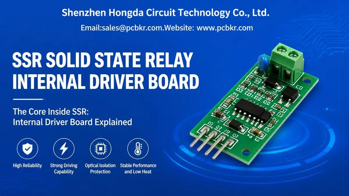
SSR Solid State Relay Internal Driver Board: PCB Manufacturing and Quality Control
PCB Material: FR-4 / High-Tg FR-4
Layers: 2–6 Layers
Board Thickness: 0.8–2.0 mm
Copper Thickness: 1–2 oz
Min. Trace Width / Spacing: 0.10 / 0.10 mm
Min. Hole Size: 0.20 mm
An SSR Solid State Relay Internal Driver Board must do more than connect electronic components. Its PCB layout, insulation boundaries, copper geometry, component assembly, and electrical verification all influence whether the driver circuit operates consistently in its intended application. For PCB and PCBA manufacturers, the key responsibility is to translate the customer’s circuit design into controlled manufacturing requirements without changing the electrical design or making unsupported safety assumptions.
This guide explains how to review an SSR driver board before production, control the PCB fabrication and assembly processes, and verify manufacturing quality. It focuses on practical checks that a PCB manufacturer can perform using the customer’s approved design files, specifications, and test requirements.
What Should a PCB Manufacturer Review on an SSR Internal Driver Board?
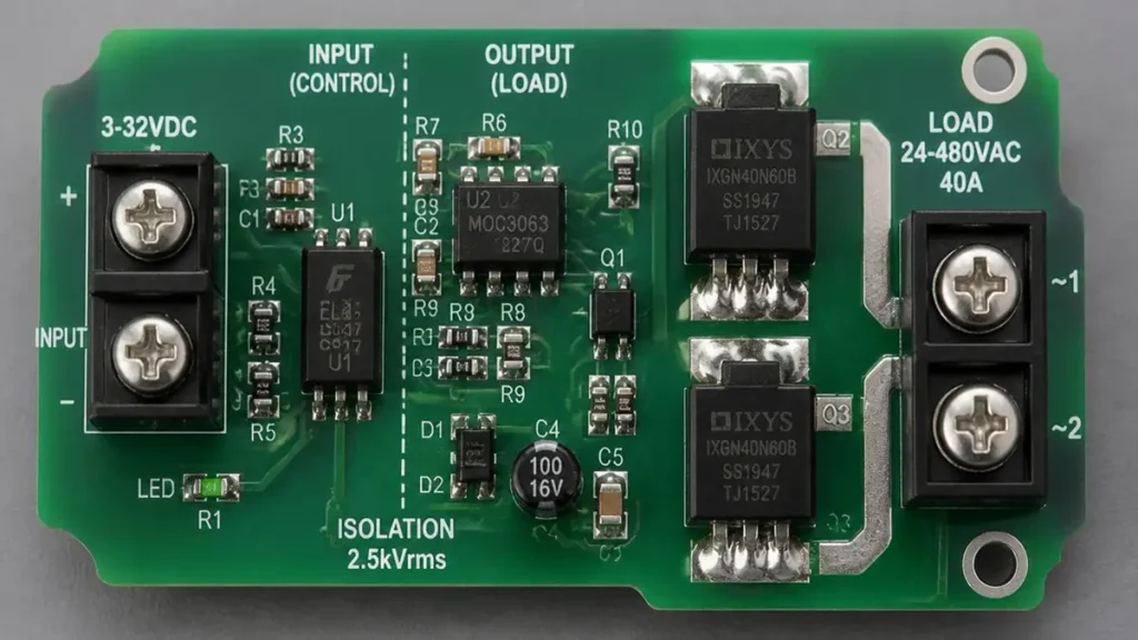
An SSR internal driver board may contain input conditioning, an isolation interface, a gate-drive circuit, protection components, auxiliary power, and monitoring functions. The exact architecture depends on whether the design uses discrete components, an integrated solid-state relay device, or a separate control board and power stage.
A PCB manufacturer should first identify the board’s functional zones from the schematic, netlist, PCB layout, and BOM. This review is not intended to redesign the circuit. Its purpose is to identify manufacturing risks that could affect the approved electrical design.
| Functional area | Manufacturing review | Potential production risk |
|---|---|---|
| Control input | Connector orientation, polarity, pin spacing, and solderability | Incorrect connection or intermittent input |
| Signal conditioning | Resistor and capacitor values, footprints, and placement | Wrong component or assembly variation |
| Isolation interface | Isolation boundary, copper keep-out, slots, and component spacing | Reduced physical separation |
| Gate-drive section | IC orientation, gate-related routing, local decoupling, and solder joints | Unstable or incorrect drive connection |
| Protection circuit | TVS, snubber, resistor, and capacitor footprints and polarity where applicable | Incorrect protection component assembly |
| Auxiliary power | Power input polarity, regulator footprint, and power/ground connections | Startup or supply instability |
| Output interface | Terminal footprint, pin assignment, copper connection, and mechanical support | Connection or thermal stress |
The review should produce a documented list of design questions, manufacturing observations, and customer-approved resolutions before production release.
A useful distinction is essential: a PCB manufacturer can identify a clearance conflict, an incorrect footprint, or an assembly risk, but should not independently change the customer’s protection threshold, isolation rating, or circuit topology.
How Should Creepage and Clearance Be Reviewed on an SSR PCB?
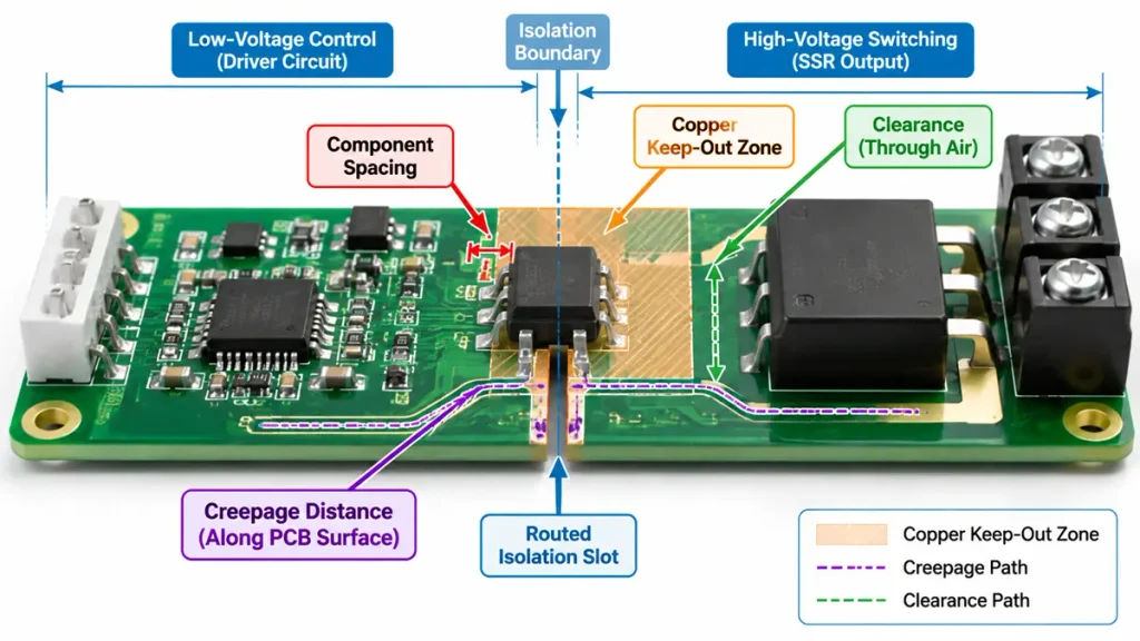
SSR PCB Creepage and Clearance Inspection
Isolation is one of the most important manufacturing review areas for an SSR driver board. The PCB must preserve the separation defined by the approved design between circuits operating at different electrical potentials.
Creepage is the shortest distance along an insulating surface. Clearance is the shortest distance through air. Both must be evaluated according to the applicable product standard and the actual electrical and environmental conditions.
A manufacturer should not apply one universal spacing value to every SSR board. The required distances depend on factors such as working voltage, transient overvoltage, pollution degree, material group, altitude, and the required insulation level.
Practical PCB manufacturing checks include:
- Isolation boundary verification: Compare the PCB copper layers and component placement with the approved isolation boundary shown in the design documentation.
- Copper keep-out inspection: Check whether copper features, pads, vias, planes, or exposed conductors encroach into specified isolation areas.
- Slot and cutout verification: Confirm that routed slots and isolation openings match the released fabrication data, including their dimensions and positions.
- Solder mask review: Do not treat solder mask as a substitute for required creepage or clearance. The approved insulation design must remain valid without relying on an assumed solder-mask barrier.
- Component spacing inspection: Check component bodies, leads, pads, and solder fillets near the isolation boundary.
- Layer-to-layer review: Check the relevant internal copper geometry and dielectric construction where the isolation requirement applies through the PCB stack-up.
The manufacturer should record any suspected violation and request written customer approval before modifying the fabrication data.
A useful release record includes the approved PCB revision, isolation boundary reference, identified clearance concerns, slot dimensions, and the customer’s disposition of each finding.
How Do PCB Layout and Copper Geometry Affect SSR Driver Board Manufacturing?
The copper layout of an SSR board must be reviewed according to the actual current paths and electrical functions. A low-voltage control trace, a gate-drive connection, an auxiliary power rail, and a high-current output path do not have the same manufacturing requirements.
The first task is to determine whether the board contains only the driver circuit or also carries the switched load current. This distinction directly affects copper thickness, trace width, thermal management, terminal design, and fabrication controls.
Gate-drive and signal routing
For boards using discrete MOSFETs or IGBTs, the manufacturer should check that the gate-drive connections, source or emitter reference connections, and related return paths match the released layout.
Where the design specifies separate gate and power-current paths, the PCB manufacturer should preserve those connections rather than merge or reroute them for convenience.
The review should include:
- Gate-driver IC footprint and pin mapping
- Gate resistor and local decoupling capacitor placement
- Connector and test-point assignments
- Trace-width and copper-clearance compliance
- Via count and via location on critical connections
- Polarity and orientation of protection components
These are manufacturing and design-for-manufacturing checks. The manufacturer should not claim that a visual layout review alone proves immunity to switching noise or guarantees stable gate-drive performance.
Copper thickness and current-carrying paths
Copper thickness should be selected according to the current carried by the specific PCB net, allowable temperature rise, copper distribution, ambient conditions, and the customer’s electrical requirements.
If the SSR driver board carries only control and gate-drive signals, it should not automatically be specified as a heavy-copper power board. If the power switching current also passes through the PCB, the manufacturer must review the relevant copper paths, terminal interfaces, thermal conditions, and fabrication tolerances.
The PCB fabrication drawing should define the required finished copper thickness where applicable. The manufacturer should also clarify whether the specified copper value refers to base copper or finished copper, since these are not interchangeable.
Thermal and mechanical considerations
Where power components or high-dissipation parts are mounted on the PCB, review the specified copper area, thermal vias, component footprint, mounting arrangement, and mechanical support.
The manufacturer can verify that the released copper features and drilled holes are fabricated as specified. Actual junction temperature, thermal resistance, and operating lifetime require circuit-level and system-level validation under defined conditions.
Which PCB Fabrication Processes Matter for SSR Driver Board Reliability?
The fabrication process should be controlled around the board’s actual design risks rather than around a generic list of advanced PCB capabilities.
| Fabrication process | Manufacturing control | Evidence or inspection record |
|---|---|---|
| Imaging and etching | Trace width, spacing, isolation keep-out, and pattern integrity | AOI results and dimensional inspection |
| Drilling | Hole diameter, position, and registration | Drill data review and hole inspection |
| Plated through holes | Copper plating continuity and finished hole requirements | Microsection or plating records when specified |
| Lamination | Stack-up construction, bonding, and layer registration | Stack-up records and cross-section where required |
| Solder mask | Defined openings, coverage, and registration | Solder-mask inspection |
| Surface finish | Finish type and solderability requirements | Process and material records |
| Routing and profiling | Board outline, slot position, edge quality, and mechanical dimensions | Profile inspection |
Why isolation features require special process attention
A narrow isolation region may contain copper keep-outs, routed slots, or specific component spacing requirements. If the PCB fabrication process shifts a slot, leaves copper too close to a boundary, or changes the finished geometry, the board may no longer match the approved design.
For this reason, isolation-related features should be treated as controlled characteristics during CAM review and first-article inspection.
Where the customer specifies critical dimensions, the manufacturer should define the inspection method and acceptance criteria before production. A general AOI pass does not replace dimensional verification of every safety-critical feature.
Why stack-up and material selection should be confirmed
The PCB material and stack-up should be based on the customer’s electrical, thermal, mechanical, and applicable insulation requirements. The manufacturer should verify the approved material grade, finished board thickness, copper construction, and dielectric arrangement.
If the design specifies a particular laminate, flammability classification, CTI-related material property, or other material requirement, the purchasing and engineering teams should confirm the exact material documentation before production.
A substitute material should not be introduced solely because it is easier to source. Any substitution that could affect insulation, thermal performance, or compliance must be reviewed and approved by the customer.
What Assembly Controls Are Required for SSR PCBA Manufacturing?
SSR driver board assembly may include small passive components, optocouplers or isolators, gate-driver ICs, MOSFETs, TVS diodes, connectors, and power components. The assembly process must preserve the approved component identity, orientation, and electrical connections.
Before SMT production, the manufacturer should verify:
- BOM part numbers against the approved revision
- Footprint compatibility between the BOM and PCB
- Pin-1 marking and polarity for ICs and diodes
- Package dimensions and component height
- Approved alternates and lifecycle status
- Connector orientation and mechanical clearance
- Special handling requirements stated by the component manufacturer
During assembly, the manufacturer should control:
- Solder paste printing and stencil alignment
- Component placement accuracy
- Reflow profile according to component and solder-paste requirements
- Polarity and orientation of polarized components
- Through-hole soldering for terminals and other THT components
- Prevention of solder bridges, insufficient solder, and lifted leads
- Cleaning requirements where residues could affect the customer’s design or application
A component substitution must be traceable to an approved alternate. The manufacturer should not replace an optocoupler, gate driver, TVS diode, or other protection-related component based only on package similarity.
For mixed SMT and THT assemblies, the production sequence should also account for connector mechanical strength, solder joint accessibility, and any customer-defined inspection requirements.
Which Quality Tests Should Be Used for SSR Driver Board PCBA?
No single inspection method can prove that an SSR driver board is safe and fully functional. PCB fabrication inspection, assembly inspection, electrical testing, and application-level validation answer different questions.
A practical quality plan separates these verification levels.
| Verification stage | Typical method | What it can verify | Important limitation |
|---|---|---|---|
| Bare PCB inspection | AOI and dimensional inspection | Pattern defects, geometry, specified critical dimensions | Does not prove circuit function |
| Internal structure verification | Microsection when specified | Plating, layer construction, and internal structural features | Sample-based unless otherwise agreed |
| Assembly inspection | AOI | Component presence, polarity features, visible solder defects | Cannot detect every hidden joint defect |
| Hidden-joint inspection | X-ray where applicable | Selected hidden solder connections, such as relevant bottom-terminated packages | Not required for every package or board |
| Electrical connectivity | ICT or flying-probe test | Opens, shorts, and accessible component or net checks according to test coverage | Coverage depends on test access and program |
| Functional verification | Customer-approved functional test | Defined input, drive, status, and output behavior | Does not automatically establish safety certification |
| Insulation verification | Customer-specified insulation or dielectric test | Insulation performance under the specified test conditions | Test voltage and method must be approved for the design |
What should an SSR functional test cover?
A functional test should be based on the released schematic, test specification, and intended board configuration.
Depending on the design, the test plan may include:
- Applying the specified control input and verifying the expected driver response.
- Checking the defined ON and OFF states at accessible test points.
- Verifying status or fault outputs where these functions are present.
- Checking auxiliary supply voltage and current against the approved limits.
- Confirming the expected response of protection or monitoring circuits when the customer provides a safe and approved test method.
If the power switching stage is on the same PCB, the test plan may also need a controlled load, switching waveform, thermal, or output-state verification. If the board is only an internal driver board, these system-level tests may belong to the customer’s final SSR assembly process rather than the PCB manufacturer’s standard PCBA test.
How should insulation testing be handled?
The test voltage, duration, ramp, trip limit, and test connections must be specified by the customer or the applicable approved test procedure.
A manufacturer should not invent a hipot voltage based solely on the nominal operating voltage or copy a value from an unrelated SSR reference design. The test must also account for components connected across the isolation boundary, protection devices, and the possibility that a test could damage sensitive circuitry.
The test report should identify the board revision, sample or serial number, test conditions, measured result, acceptance criteria, and pass/fail status.
What Causes SSR Driver Board Failures, and What Can a PCB Manufacturer Prevent?
An SSR that fails to turn off, triggers unexpectedly, overheats, or behaves inconsistently does not necessarily have a PCB manufacturing defect. The root cause may originate in circuit design, component selection, installation, operating conditions, or assembly quality.
The manufacturer’s role is to identify and control the causes that are within its production responsibility.
| Observed problem | Possible engineering cause | PCB/PCBA manufacturing review |
|---|---|---|
| SSR does not turn OFF | Input leakage, output leakage, noise coupling, or circuit-specific behavior | Verify component values, assembly, routing, and approved test results |
| Unexpected triggering | Noise coupling or inadequate separation of signal and power paths | Check layout revision, isolation boundaries, and component placement |
| Intermittent operation | Solder defects, connector issues, or component variation | Inspect solder joints, connector assembly, and component traceability |
| Excessive heating | Power dissipation, thermal design, load conditions, or poor connection | Check copper geometry, solder joints, terminals, and specified thermal features |
| Protection circuit does not respond as expected | Incorrect component, polarity, footprint, or circuit-level design issue | Verify BOM, orientation, assembly, and functional test coverage |
| Isolation test failure | Design spacing, contamination, fabrication damage, or test setup | Review PCB geometry, cleanliness requirements, and test configuration |
For example, an SSR may remain partially energized because of leakage current or an input-side drive condition. That does not automatically indicate a defective PCB. The manufacturer should verify the assembled components and the specified electrical behavior, then provide the inspection and test evidence needed for engineering fault isolation.
This distinction is important for reliable failure analysis. Replacing a board without identifying whether the cause was design-related, component-related, or manufacturing-related may allow the same problem to recur.
How Should Buyers Evaluate an SSR PCB and PCBA Manufacturer?
A capable SSR PCB supplier should demonstrate more than general PCB fabrication experience. Buyers should assess whether the supplier can understand the board’s functional zones, preserve isolation-related geometry, control component assembly, and provide traceable inspection results.
During supplier evaluation, ask for evidence in the following areas:
| Supplier evaluation area | Questions buyers should ask | Evidence to request |
|---|---|---|
| Engineering review | Can the supplier review Gerber, BOM, schematic, and assembly drawings together? | DFM feedback and engineering review records |
| Isolation-related fabrication | Can the supplier identify and control specified isolation boundaries, slots, and copper keep-outs? | CAM review and dimensional inspection records |
| PCB process control | How are trace geometry, drilling, plating, and stack-up controlled? | Fabrication specifications and relevant inspection reports |
| Component sourcing | Are substitutions controlled through customer approval? | BOM reconciliation and traceability records |
| SMT/THT assembly | How are polarity, placement, soldering, and mixed-technology assembly inspected? | AOI, X-ray where applicable, and process inspection records |
| Electrical testing | Can the supplier provide the test coverage required by the project? | ICT, flying-probe, or functional test reports |
| Quality traceability | Can production lots and inspection results be traced to the released revision? | Lot records, revision history, and final inspection reports |
A supplier should also explain which tests are included in standard production and which require a separate fixture, test program, sample quantity, or customer-approved procedure.
For projects that include a separate auxiliary power section, buyers may also review the supplier’s experience with PCB manufacturing for power supply applications. If the SSR board integrates a high-current switching path, heavy copper PCB manufacturing may also be relevant. These capabilities should be evaluated only when the actual board design requires them.
What Information Should Buyers Provide for an SSR Driver Board RFQ?
A complete RFQ package helps the manufacturer evaluate manufacturability, material requirements, assembly complexity, test coverage, and production cost.
Buyers should provide:
- Gerber or ODB++ fabrication data
- PCB stack-up and fabrication drawing
- Schematic and netlist, where available
- BOM with manufacturer part numbers
- Pick-and-place file and assembly drawing
- Board quantity and expected production volume
- Required PCB material, thickness, and copper specification
- Defined isolation requirements and relevant standards
- Test requirements, including functional and insulation test conditions
- Approved component alternates and sourcing restrictions
- Packaging, labeling, and traceability requirements
If the project is still at prototype stage, the buyer should identify which specifications are fixed and which remain open for engineering review. This allows the manufacturer to separate confirmed production requirements from items that need customer clarification.
Request an SSR PCB/PCBA manufacturing review
Send your Gerber or ODB++ files, BOM, assembly drawing, and available test specifications for a manufacturing review and quotation. The engineering team can evaluate PCB fabrication, SMT/THT assembly, and the inspection requirements supported by the project documentation.
Email: sales@pcbkr.com
Website: www.pcbkr.com
FAQs About Choosing an SSR PCB and PCBA Manufacturer
What should I look for in an SSR driver board PCB manufacturer?
Look for a manufacturer that can review the PCB layout, isolation boundaries, copper geometry, material requirements, and assembly documentation together. Ask for evidence of CAM/DFM review, fabrication inspection, SMT/THT process control, and electrical test capability. The supplier should also explain which tests are included in the quotation and which require separate customer specifications.
Can a PCB manufacturer verify creepage and clearance on an SSR board?
A PCB manufacturer can inspect the specified creepage and clearance features against the approved design and fabrication data. However, determining the required safety distances depends on the working voltage, insulation category, pollution degree, material properties, altitude, and applicable product standard. The customer or responsible design authority must define and approve the required insulation criteria.
Does SSR driver board PCBA production require AOI, X-ray, and ICT?
The inspection plan depends on the component packages, board design, and customer requirements. AOI is commonly used to inspect visible assembly features. X-ray may be appropriate for selected hidden solder joints. ICT or flying-probe testing can check electrical connectivity within the available test coverage. None of these methods alone proves complete SSR functionality or product safety.
Can a PCBA manufacturer perform hipot testing on an SSR driver board?
Yes, if the manufacturer has an appropriate test setup and the customer provides an approved test specification. The required test voltage, duration, connections, and acceptance limits must be defined for the actual board and its components. A generic hipot value should not be applied to every SSR design.
What files are required to quote an SSR Solid State Relay Internal Driver Board?
A useful RFQ package includes Gerber or ODB++ data, PCB fabrication drawing, stack-up, BOM with manufacturer part numbers, pick-and-place file, assembly drawing, schematic where available, quantity, and required inspection or electrical test specifications. Clear isolation and functional test requirements help the supplier assess the project accurately before production.
About Author
David Chen LinkedIn Profile
David Chen is a Senior RF/PCB Process Engineer at Shenzhen Hongda Circuit Technology Co., Ltd., with over 12 years of experience in high-frequency PCB fabrication, impedance-controlled stack-up design, and Rogers/PTFE laminate processing. He also boasts an extensive professional background in PCBA manufacturing, PCBA testing, and PCBA optimization, with specialized expertise in high-precision PCBA fault analysis and rigorous PCBA reliability testing. The author has worked with high-layer-count server PCB fabrication, ultra-low-loss backplane stackups, and thermo-mechanical reliability optimization for AI infrastructure projects involving 112G and 224G PAM4 architectures. Skilled in complex circuit design and cutting-edge advanced PCB manufacturing processes, he delivers solutions that elevate product durability and performance across industrial applications. His technical articles focusing on PCBA manufacturing workflows and testing methodologies are widely cited by industry peers and technical platforms, and have gained attention and recognition from industry colleagues.
SSR Solid State Relay Internal Driver Board – Data Sheet
| Parameter | Specification |
|---|---|
| PCB Material | FR-4 / High-Tg FR-4 |
| PCB Layers | 2–6 Layers |
| Board Thickness | 0.8–2.0 mm |
| Copper Thickness | 1–2 oz |
| Minimum Trace Width / Spacing | 0.10 / 0.10 mm |
| Minimum Hole Size | 0.20 mm |
| Surface Finish | HASL / Lead-Free HASL / ENIG |
| Solder Mask | Green / Blue / Black / White |
| Silkscreen | White / Black |
| PCB Technology | Through-Hole / Multilayer PCB |
| Assembly Technology | SMT / THT / Mixed Assembly |
| Component Types | Optocouplers, Gate Drivers, MOSFETs, TVS Diodes, Resistors, Capacitors, Connectors |
| Isolation Features | Copper Keep-Out Areas / Isolation Slots, According to Design Requirements |
| Assembly Inspection | AOI / X-ray (Where Applicable) |
| Electrical Testing | ICT / Flying Probe / Functional Testing |
| Special Testing | Insulation or Dielectric Withstand Testing, According to Customer Specifications |
| Applications | AC SSR Driver Boards / DC SSR Driver Boards / Industrial Solid-State Relay Control Systems |
Technical Note:
The specifications above are indicative reference values for PCB and PCBA quotation purposes, not fixed specifications for every SSR driver board. Final material selection, layer count, board thickness, copper thickness, trace width/spacing, hole size, isolation geometry, and testing requirements must be confirmed according to the Gerber or ODB++ files, BOM, circuit architecture, working voltage, and customer technical specifications.
Creepage, clearance, insulation, and dielectric withstand requirements must be defined according to the applicable product standard and approved design. Optional inspection and testing items depend on the specific project and do not necessarily apply to every board.