Why Are AI Server PCBs More Expensive Than Traditional PCBs?
AI server PCBs are dramatically more expensive because they combine ultra-high-speed signaling, extreme power density, advanced materials, complex multilayer manufacturing, and much stricter reliability requirements than conventional PCBs. In many real-world deployments, AI server boards cost 3–10× more than traditional server PCBs due to compounded engineering and fabrication challenges.
As AI infrastructure expands globally, PCB manufacturing has entered a new era where the board itself becomes part of the compute architecture. Modern GPU clusters, AI accelerator backplanes, and high-bandwidth networking systems now require telecom-grade signal integrity, semiconductor-level process precision, and supercomputer-class thermal management.
Key Industry Observation:
Traditional server boards were primarily constrained by logic functionality and moderate thermal density. AI server PCBs, however, are constrained simultaneously by signal integrity, power delivery, mechanical stability, material loss characteristics, and long-term thermal reliability.
What Makes an AI Server PCB Different?
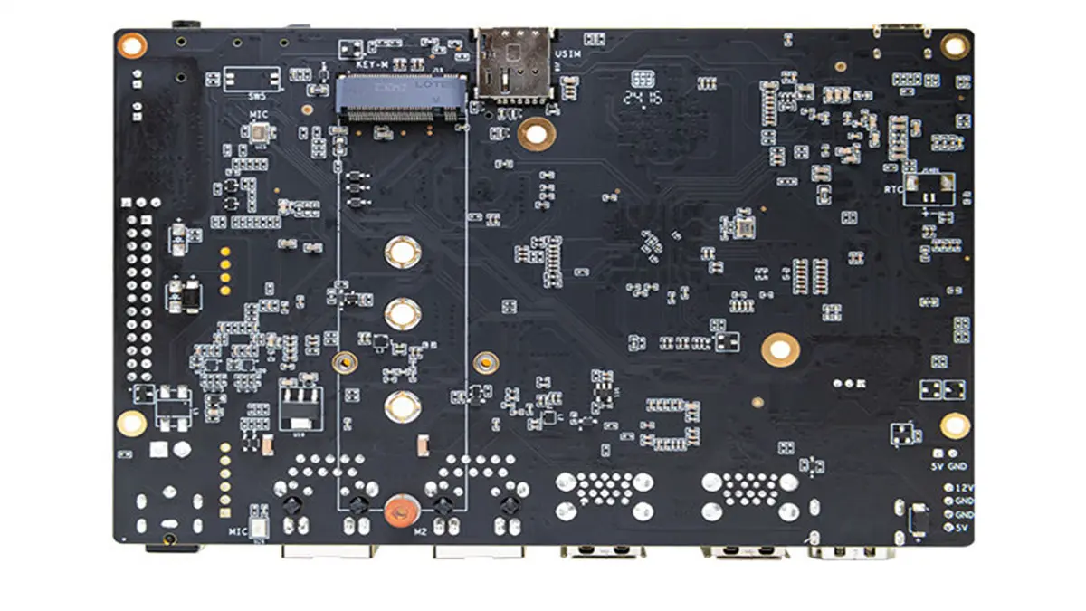
AI server PCBs operate at far higher bandwidth, power density, thermal load, and routing complexity than traditional PCBs. These boards are commonly used in GPU training clusters, TPU systems, AI networking switches, and HBM accelerator modules.
| Parameter | Traditional Server PCB | AI Server PCB |
|---|---|---|
| Typical Layer Count | 8–16 Layers | 16–40+ Layers |
| Signal Speed | 10–25G NRZ | 112G/224G PAM4 |
| Material Type | Standard FR4 | Megtron 6/7, Rogers, VT-901 |
| Power Density | Moderate | Extremely High |
| Typical Cost | $50–$200 | $1,500–$8,000+ |
In many 112G PAM4 systems, the PCB itself becomes part of the high-speed transmission environment. Minor dielectric instability, layer misregistration, or via stub resonance that once had minimal impact in conventional servers can now directly trigger bit error rate degradation, retraining instability, or channel collapse.
Why Do Advanced Materials Increase AI PCB Costs So Much?
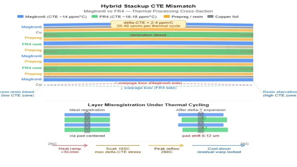
hybrid-stackup-cte-mismatch-megtron-fr4
AI server PCBs require ultra-low-loss dielectric materials because standard FR4 introduces excessive insertion loss at high data rates. Platforms using PCIe Gen 5/6, 112G PAM4, and next-generation AI fabrics demand low-Dk and low-Df laminates capable of maintaining signal integrity over long channels.
- Panasonic Megtron 6 and Megtron 7
- Rogers high-frequency laminates
- Ventec VT-901
- Isola Tachyon materials
These materials are significantly more expensive than standard FR4 and often require hybrid stackups that combine multiple resin systems within one multilayer PCB.
Manufacturing Pain Point:
Hybrid stackups dramatically increase lamination complexity because different laminate systems expand and contract differently during thermal processing. This creates severe registration control challenges during multilayer alignment.
Why Does Layer Count and Routing Complexity Raise Costs Exponentially?
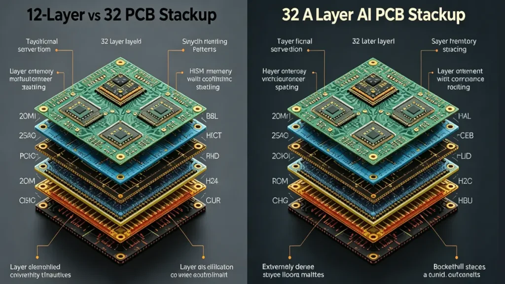
12-Layer vs 32-Layer AI PCB Stackup
Traditional enterprise server motherboards based on Intel and AMD dual-socket platforms commonly use 8–16 layers, especially in PCIe Gen 4 and PCIe Gen 5 generations. However, AI accelerator boards frequently require 20, 28, 32, or even 40+ layers to support massive GPU interconnect density, HBM routing density, and ultra-high-speed AI fabric architectures.
Every additional layer introduces more lamination cycles, drilling complexity, copper registration challenges, inspection requirements, and scrap probability.
Key Signal Integrity Requirements
- Controlled impedance routing
- Tight differential pair skew control
- Back-drilling to remove via stubs
- Ultra-low insertion loss channels
- Reduced crosstalk
Back-drilling is particularly expensive because it requires controlled-depth drilling with extremely tight tolerance control. Thick AI boards can exceed 5–7 mm total thickness, making drill wander increasingly difficult to control.
Expert Engineering Observation:
At 112G PAM4 speeds, via stubs become resonant structures rather than simple mechanical remnants. Even several mils of residual stub length can significantly degrade eye diagrams and increase return loss.
Why Are AI PCB Manufacturing Processes Much More Difficult?
AI server PCBs demand semiconductor-like fabrication precision. Modern AI boards often require fine-line etching below 50µm, laser-drilled microvias, sequential lamination cycles, and deep via plating with aspect ratios above 12:1.
Major Manufacturing Challenges
- Fine-line etching for GPU package breakout regions
- UV and CO₂ laser drilling for microvias
- Sequential lamination processes
- Deep via copper plating uniformity
- IPC Class 3 tolerance compliance
Each sequential lamination cycle increases process complexity and dramatically raises the probability of scrap due to alignment drift, resin flow variation, or copper movement.
Real Manufacturing Scenario:
In one 32-layer AI accelerator project review, cross-sectional analysis revealed localized copper thinning near buried via corners after thermal cycling. The root cause was plating current crowding during fabrication combined with high aspect ratio via geometry.
Why Do Thermal and Power Requirements Increase PCB Costs?

IR thermal imaging map of an AI GPU PCB, highlighting the intense core hotspot and localized thermal stress caused by high power density
Modern AI GPUs can consume 600W–1000W or more, forcing PCB designers to manage extreme current density and localized thermal stress.
- 3–6 oz heavy copper planes
- Thermal via arrays
- Embedded copper heat spreaders
- Advanced PDN structures
- Warpage-resistant stackups
Even tiny resistance variations inside high-current power planes can generate severe localized heating under AI training workloads.
Large AI boards exceeding 600 mm also experience significant reflow warpage risk due to asymmetric copper distribution and mixed-material stackups.
Thermal Reliability Risk:
Excessive PCB warpage can trigger BGA solder cracking, head-in-pillow defects, connector misalignment, and intermittent GPU failures during long-term AI training operation.
Why Is Testing and Qualification So Expensive for AI PCBs?
Traditional electrical continuity testing is no longer sufficient for modern AI server boards. Advanced AI PCBs require extensive signal integrity validation, thermal reliability qualification, and process traceability.
- Automated Optical Inspection (AOI)
- X-ray CT scanning
- TDR impedance validation
- VNA insertion-loss testing
- Thermal cycling qualification
- Burn-in reliability testing
Hyperscaler customers often require multi-month qualification programs involving environmental stress testing, reliability audits, and statistical process control documentation.
Industry Reality:
In many AI infrastructure projects, qualification and validation time can exceed the actual PCB fabrication cycle itself.
Why Do Supply Chain Constraints Push AI PCB Prices Higher?
Only a limited number of global manufacturers possess the process capability required for advanced AI server PCB fabrication.
- TTM Technologies
- Tripod Technology (健鼎)
- Shennan Circuits (深南电路)
- WUS Printed Circuit (沪士电子)
- Sytech / Shengyi Electronics (生益电子)
- Gold Circuit Electronics / GCE (金像电)
- AT&S
Advanced laminate supply is also concentrated among relatively few companies, creating structural bottlenecks across materials, HDI capacity, laser drilling infrastructure, and testing capability.
Industry Capability Shift:
Beyond multinational Tier-1 PCB giants, specialized manufacturers with strong high-layer-count capability, fine-line processing expertise, and strict back-drill process control are becoming increasingly important in the global AI hardware supply chain. Companies such as Shenzhen Hongda Circuit Technology Co., Ltd. (PCBKR) represent a growing category of advanced PCB manufacturers capable of supporting complex AI server and accelerator board requirements.
Geopolitical factors such as export controls, regional manufacturing concentration, and AI infrastructure competition further amplify pricing pressure and lead-time volatility.
How Much More Expensive Are AI Server PCBs?
| PCB Type | Indicative Cost Range |
|---|---|
| Standard Server PCB | $50–$200 |
| Telecom Backplane | $500–$2,000 |
| AI Accelerator PCB | $1,500–$8,000+ |
| AI Networking Switch Board | $3,000–$10,000+ |
Although these numbers appear high, the PCB itself often represents only 5–12% of the total AI server BOM. Reliability is prioritized over minimal PCB cost because a single PCB failure can disable extremely expensive AI compute infrastructure.
Could AI Server PCB Costs Fall in the Future?
Several emerging technologies may eventually reduce AI PCB manufacturing cost over the next 3–7 years.
- Low-shrinkage resin systems for improved dimensional stability
- Advanced LDI/CCD optical alignment systems
- Semi-additive PCB manufacturing processes (SAP/mSAP)
- AI-assisted PCB routing optimization
- Localized advanced PCB fabrication investments
- Glass substrate technologies for future advanced packaging ecosystems
However, in practical 2026 manufacturing environments, the most immediate industry focus is not glass substrate commercialization at the PCB board level, but rather improving dimensional stability and reducing warpage through new low-shrinkage resin systems and more advanced automated optical alignment technologies.
2026 Industry Trend:
Many advanced AI PCB manufacturers are now investing heavily in high-precision LDI (Laser Direct Imaging) and CCD-based optical registration systems because multilayer alignment accuracy has become one of the primary yield bottlenecks for 28–40 layer AI accelerator boards.
Large-scale cost reductions will still require major improvements in material availability, fabrication yield, HDI process maturity, and global manufacturing capacity.
Conclusion
AI server PCBs are more expensive because multiple engineering and manufacturing challenges compound simultaneously. Advanced materials, multilayer complexity, HDI routing, thermal management, precision fabrication, extended qualification cycles, and supply-chain bottlenecks collectively drive costs far beyond those of traditional PCBs.
As AI infrastructure deployment accelerates globally, advanced PCB manufacturing capacity will become one of the most critical bottlenecks in the next generation of high-performance computing systems.
Why are AI server PCBs much more expensive than gaming PC motherboards?
AI server PCBs require far higher layer counts, low-loss materials, extreme thermal management, and telecom-grade signal integrity compared with consumer gaming boards.
Why do AI server PCBs require low-loss materials instead of FR4?
Standard FR4 introduces excessive insertion loss at 112G+ PAM4 signaling speeds, while low-loss laminates preserve signal integrity over long channels.
Why does back-drilling increase PCB manufacturing cost?
Back-drilling requires controlled-depth drilling with extremely tight tolerance control, especially in thick multilayer AI boards.
Why are AI PCB qualification cycles so long?
Hyperscalers require extensive thermal, electrical, and reliability validation because PCB failures can destabilize extremely expensive AI clusters.
Why can’t most PCB factories manufacture AI server boards?
Advanced AI server PCBs require HDI capability, laser drilling systems, precision lamination, SI validation expertise, and high-yield process control that many standard PCB factories do not possess.
Using top-tier AI server PCB equipment to manufacture traditional PCBs delivers a strategic advantage: interlayer alignment tolerance shrinks from ±75μm to within ±25μm, and differential impedance control tightens to ±5%. Paired with 100% 3D X-Ray inspection, it grants conventional boards chip-level precision, superb signal stability, and near-100% yield.
Still, need help? Contact Us: sales@pcbkr.com
Need a PCB or PCBA quote? Quote now
About Author
David Chen https://www.linkedin.com/in/pcbcoming/
David Chen boasts an extensive professional background in PCBA manufacturing, PCBA testing, and PCBA optimization, with specialized expertise in high-precision PCBA fault analysis and rigorous PCBA reliability testing. Skilled in complex circuit design and cutting-edge advanced PCB manufacturing processes, he delivers solutions that elevate product durability and performance across industrial applications. His technical articles focusing on PCBA manufacturing workflows and testing methodologies are widely cited by industry peers, research institutions, and technical platforms, solidifying his reputation as a recognized technical authority in the global circuit board manufacturing sector.