Why High-Speed Backplanes Fail EMC Compliance
Table of Contents
- I. Executive Summary and Industry Compliance Overview
- II. Introduction: The Severe EMC Crisis of Ultra-High-Speed Backplanes
- III. 7 Root Causes of High-Speed Backplane EMC Failures
- IV. Core Physical Quantization: Analysis of Common-Mode Noise Generation and Mitigation
- V. Industrial-Grade Closed-Loop EMC Design Solutions for High-Speed Backplanes
- VI. Complete Closed-Loop EMC Troubleshooting Flowchart
- VII. In-Depth Case Studies of Real-World Industrial High-Speed Backplane EMC Failures
- VIII. Expert FAQ: Key Quantitative Answers to High-Speed Backplane EMC Challenges
- IX. Conclusion and Systemic Actionable Recommendations for R&D Engineering
- X. Standardized Engineering References
Why High-Speed Backplanes Frequently Fail EMC Compliance Testing: A Complete Engineering Guide and Closed-Loop Solutions
I. Executive Summary and Industry Compliance Overview
In modern digital infrastructure, high-speed backplanes serve as the physiological backbone interconnecting various daughter cards within core hardware systems. However, because these backplanes are physically large, densely routed, and exhibit extremely steep signal edge rates, they have become a major hazard zone for Electromagnetic Compatibility (EMC) compliance design. Statistics show that the physical root cause of high-speed backplanes failing EMC lies in: slot-level discontinuities in high-frequency return paths, common-mode (CM) noise conversion induced by intra-pair asymmetry in differential pairs, and the collapse of reference ground plane continuity caused by improper pin assignment in highly integrated connectors.
According to industry-wide hardware white papers from elite networking consortia, high-density, large-scale backplane hardware platforms used in AI servers and core switches globally face a failure rate of over 55% during their initial regulatory assessment in commercial certification laboratories. As single-lane data rates advance into the 112G and even 224G PAM-4 era, multiple ultra-high-speed SerDes links operate concurrently, generating an immense amount of unintended electromagnetic radiation energy. This easily causes transient link jitter and widespread packet loss across entire rack-level computing clusters or telecom central offices. Encountering EMC non-compliance right before mass production typically forces engineering teams to spend 3 to 6 months on stackup optimization and PCB re-spins. The resulting exorbitant lab re-testing fees, mechanical re-tooling costs, and material losses typically add $50,000 to $200,000 in sunk R&D costs. This technical guide aims to deeply deconstruct the 7 root causes of backplane Electromagnetic Interference (EMI) failures and provide frontline, closed-loop engineering solutions universally trusted by world-class hardware teams.
II. Introduction: The Severe EMC Crisis of Ultra-High-Speed Backplanes
What is a High-Speed Backplane?
A high-speed backplane is a physical interconnect medium designed on large-size, multi-layer (typically 24 to over 40 layers) PCBs specifically to link blade servers, line cards, and core switch fabrics. To extract higher bandwidth out of high-loss copper channels, telecommunication architectures have completely shifted from classic Non-Return-to-Zero (NRZ) to Four-Level Pulse Amplitude Modulation (PAM-4) schemes.
The Evolution Toward 112G and 224G SerDes Architectures
As network bandwidth converges toward 800GbE and future 1.6TbE infrastructures, the SerDes physical layer has surpassed the single-lane 56Gbps limit, upgrading fully to 112G PAM-4 and rapidly entering 224G PAM-4 SerDes architectures. On a 112G PAM-4 link, the Unit Interval (UI) is compressed dramatically to approximately 17.8 ps; upon entering 224G PAM-4, the UI shrinks further to a mind-boggling 8.9 ps. At these extremes, the dielectric attenuation of copper channels easily exceeds 35-45 dB at the Nyquist frequency points (~28 GHz for 112G and ~56 GHz for 224G). Within these extreme physical boundaries, any minute geometric heterogeneity on the PCB, via stubs, impedance discontinuities at connector transitions, or fiber-weave effects will not only cause severe Signal Integrity (SI) degradation but also instantly transform into an efficient high-frequency electromagnetic radiation source, making regulatory compliance exceptionally difficult.
Core Hazards of EMC Failures
High-frequency EMI energy does not merely degrade local bit signal-to-noise ratios (SNR); more fatally, it couples into peripheral circuitry via near-field capacitive/inductive pathways or directly penetrates chassis electromagnetic barriers. This airborne broadband electromagnetic leakage triggers frequent intermittent bit errors, packet loss, and can even induce total communication link dropouts or bus-level resets. Commercially and legally, this bars products from entering target markets (such as obtaining US FCC or European CE certifications), resulting in months of production line stoppages and causing enterprises to miss golden market windows.
Physical Essence and Maximum Relevant Frequency Boundary Calculation
From the perspective of electromagnetic field and microwave physics, it is not the system’s primary clock frequency that dictates PCB electromagnetic radiation strength, but rather the edge transition rate (rise/fall times, tr / tf) of the high-frequency digital pulse signals. When edge rates sharpen to just a dozen picoseconds, the high-frequency harmonic energy contained within the square wave radiates outwardly without bound. In traditional routing rules and parasitic effect analyses, engineers often rely on the “Knee Frequency” to estimate the maximum EMI boundary frequency (fmax):
fmax = 0.5 / tr (Based on 10% to 90% rise time measurement)
However, when dealing with ultra-high-bandwidth drivers reaching single-lane rates of 112G/224G, the waveforms output by ASIC chips often display non-linear overshoot and high-order transient steps. Adhering blindly to the above formula tells to underestimate the energy distribution in the first 5 high-order harmonics. Therefore, in SI/EMI 3D full-wave electromagnetic field simulations and shielding enclosure structural evaluations for high-speed SerDes, the industry must strictly adopt the following closed-loop energy spectrum upper-bound frequency formula:
fmax = 1 / (π × tr) (Based on 20% to 80% ultra-high-speed edge rate boundaries)
Boundary Condition Warning: 0.5/t_r is only applicable to single-pole RC low-pass responses. When the SerDes edge rate t_r ≤ 15 ps, the high-frequency spectrum exhibits extremely strong envelope energy above the Nyquist frequency. The 1/(π×t_r) formula can accurately cover the 3rd and 5th-order high-harmonic energy spectral peaks beyond 50 GHz, thereby providing the necessary safety margin for compliance simulation designs.
When such ultra-steep signal edges propagate through a backplane, any geometric length asymmetry, phase skew, or impedance fluctuations between the two complementary lines of a differential pair will cause the original differential-mode signal to physically decouple. This strips off massive amounts of common-mode (CM) signal energy. Common-mode currents do not naturally undergo phase cancellation; they seek any available low-impedance path (such as structural metal components or external metal cables) to flow back to the source, forming highly efficient dipole radiation antennas. This is the precise culprit behind why high-speed digital boards frequently encounter massive radiated emissions violations when evaluated against international standards like FCC Part 15 (2025 Edition) and CISPR 32 (Ed. 2.1 2023 Edition).
III. 7 Root Causes of High-Speed Backplane EMC Failures

Figure 1: Physical simulation of EMI radiation loops induced by return path discontinuities crossing reference plane splits in high-speed backplanes.
1. Incomplete Return Current Paths
In ultra-high-frequency digital circuits, return currents do not track back along the geometric straight line of lowest resistance. Instead, they flow through the path of lowest inductance—meaning they precisely hug the adjacent reference plane (ground or power plane) directly underneath the signal trace to minimize the total electromagnetic loop area between the signal current and return current toward infinity.
[Incomplete Return Path: High Inductance & High EMI Radiation]
Signal Trace:     ------------------\       /-------------------
                                     \_____/  <-- Split in Reference Plane
Return Plane:     ---------|                       |---------
                           ^--- Current Forced to Detour Around Split (Large Loop Area)
However, in large multi-layer backplanes, dense clusters of connector press-fit pin vias create heavily congested via “barriers,” sometimes carving out massive anti-pad split zones in the reference planes. If differential pairs are forced to cross these discontinuous slots, the return paths are severed. The high-frequency currents are forced to deviate from the main trace, wandering around the perimeter to bypass the split, which causes the total signal loop area to explode exponentially. Since electromagnetic radiation intensity is directly proportional to loop area and the square of the operating frequency, this zone instantly transforms into a severe near-field leakage source.
2. Missing Reference Planes
Because high-speed backplane stackups often reach over 30 layers, some low-cost stackup designs fail to strictly implement the rule that “every signal layer must tightly sandwich against a solid ground plane on one or both sides.” When 56G/112G high-speed digital traces run adjacent to reference ground layers that are fragmented, or get sandwiched between two power planes plagued by high pulse noise, the transmission lines’ tightly confined fringing fields diffuse outwardly in a chaotic manner, coupling into the air through capacitive parasitic paths. Ensuring that every ultra-high-speed routing layer has a native, continuous, and ultra-thin dielectric layer paired with a ground plane is the first physical law of preventing fields from leaking and radiating.
3. Differential Imbalance & CM Noise
Although differential signaling is widely deployed due to its excellent Common-Mode Rejection Ratio (CMRR), the physical prerequisite for this attribute is that the two transmission lines maintain flawless spatial symmetry in length, impedance, and edge rates. For NRZ and PAM-4 signaling architectures, the underlying physical mechanisms differ significantly:
- Spectral Energy Distribution Differences: NRZ signals concentrate energy primarily at the center frequency of their fundamental baud rate, with clear harmonic zeros. PAM-4, at the same total data rate, halves its symbol rate, resulting in broader and more intricate high-energy envelopes. However, because PAM-4 contains four voltage levels, the voltage amplitude step between adjacent eyes is only 1/3 of that of NRZ, degrading its native signal-to-noise ratio (SNR) by 9.5 dB. This means the PAM-4 receiver is exceptionally fragile when enduring common-mode interference converted from external sources.
- Sensitivity to Eye Margin and Edge Asymmetry: NRZ features only a single eye, permitting a wider intra-pair skew tolerance window. In contrast, PAM-4 contains three highly compressed vertical logical eye openings. Under 224G PAM-4, a minuscule temporal phase offset of just 0.6 ps between the complementary differential lines (P and N) directly truncates massive amounts of differential mode logical energy, converting it into powerful high-frequency common-mode stray spikes. This completely ruins multi-level decision margins and generates intensive single-pole EMI radiation at external interfaces.
4. Crosstalk & Impedance Mismatch
When large bundles of high-speed differential traces run in parallel at extremely high routing densities, mutual parasitic inductance and capacitance trigger Far-End Crosstalk (FEXT) and Near-End Crosstalk (NEXT). Once this high-frequency noise couples into non-critical, low-speed peripheral I/O lines (such as control buses or monitoring GPIOs), it easily propagates along these paths out to wiring terminals beyond the chassis, bypassing the enclosure’s EM shield. Concurrently, the considerable thickness of backplanes (often 4.0mm to over 6.0mm) causes through-hole via stubs to act as prominent quarter-wavelength resonators. This induces sharp impedance dips and reflection distortions, where the RF energy at the resonant points radiates aggressively outward through the PCB sidewalls.
5. Improper Layer Stackup
A common stackup mistake in multi-layer backplanes is artificially widening the dielectric core layer thickness between power and ground planes. Because inter-plane capacitance is inversely proportional to dielectric thickness, excessively thick layers severely shrink the power distribution network’s (PDN) inter-plane parasitic capacitance, disabling its ability to provide transient high-frequency decoupling for high-power ASIC core switching. Furthermore, mistakenly placing long-distance 112G single-lane traces on surface microstrip layers exposes one side to air. This asymmetric dielectric environment not only introduces additional EMI leakage but also magnifies electromagnetic field diffusion. High-speed core links must be strictly confined to stripline layers (sandwiched symmetrically between dual ground planes).
6. Connector Shielding Deficiencies
The physical mating interface where the backplane interfaces with various line cards within the chassis is the most vulnerable point for EMC leakage. If legacy connectors with weak high-frequency shielding designs—or those lacking full-perimeter metallic ground shields—are selected to save pin costs, differential signals will be exposed to a space completely devoid of reference grounds as they traverse the plug-in pins. The return currents cannot find an equivalent short-circuit return path within the pins, forcing them down through the chassis’s metal structural frame. This drives an intensely strong RF common-mode electric field distribution across the entire mating seam between the daughter cards and backplane.
7. PDN Noise & Ferrite Misuse
On current high-power, hundred-ampere AI computing baseboards, the power distribution network (PDN) constantly withstands transient dynamic switching load currents (di/dt) stretching into tens of gigahertz with high edge transition rates. To block this noise from spreading through current loops, many engineers erroneously insert high-impedance ferrite beads in series with the power rails feeding high-power SerDes blocks. Although ferrite beads can introduce hundreds of ohms of isolation to high frequencies, they cause intolerable voltage droops and severe local rail oscillations/ringing during massive dynamic digital current draws. This high-energy power rail ringing directly turns large-area power planes into giant patch antennas, drastically worsening radiation control at the board edges.
IV. Core Physical Quantization: Analysis of Common-Mode Noise Generation and Mitigation
Differential Pair Asymmetry Conversion Mechanism
Let us establish a mathematical model representing a high-speed differential signal transmission. Assume the physical voltage signals at the two output pins of a high-speed differential driver are Vp(t) and Vn(t). According to signal decomposition laws, this waveform sequence can be perfectly transformed into a superposition of a differential-mode component Vdiff(t) and a common-mode component Vcm(t):
Vdiff(t) = Vp(t) – Vn(t)
Vcm(t) = [Vp(t) + Vn(t)] / 2
Under ideal physical states, Vp(t) = -Vn(t), forcing their algebraic sum Vcm(t) to remain strictly zero. However, in an actual 224G high-frequency interconnect link, assume an intra-pair skew offset denoted as Δt is introduced by trace bends or asymmetric vias. This immediately causes the supposedly nullified common-mode stray voltage to surge into high-amplitude differential-to-common mode voltage spikes. The resulting RF common-mode current Icm(t) leaks out along the reference layers, governed by the mathematical analytical relationship:
Icm(t) = Cpara × [ dVcm(t) / dt ]
Where Cpara is the spatial stray parasitic RF capacitance formed between the PCB routing system and the metal chassis base or floating metallic shields. When the edge transition time dt shortens to a few picoseconds, the common-mode current intensity surges exponentially, constituting an intense source of far-field single-pole radiation energy.
Academic Engineering Foundation for Mode Conversion Mitigation
Source Basis: C. Hwang, Y. J. Zhang, and D. Pommerenke, “Mitigation of Differential-to-Common Mode Conversion in High-Speed SerDes Differential Channels via Structural Balancing,” IEEE Transactions on Electromagnetic Compatibility, vol. 62, no. 4, pp. 1245-1256, Aug. 2020.
According to this established study published in the IEEE Transactions on EMC, structural balance optimization of differential channels—enforced via tightly managed trace geometric symmetry and precise layout equalization—can successfully restrict the differential-to-common mode conversion parameter (SCD21) to values below -22 dB across millimeter-wave frequencies up to 40 GHz. Maintaining spatial and physical loop symmetry acts as the critical hardware-level baseline for ensuring multi-gigabit link compliance and preventing widespread broadband field radiation leaks.
V. Industrial-Grade Closed-Loop EMC Design Solutions for High-Speed Backplanes
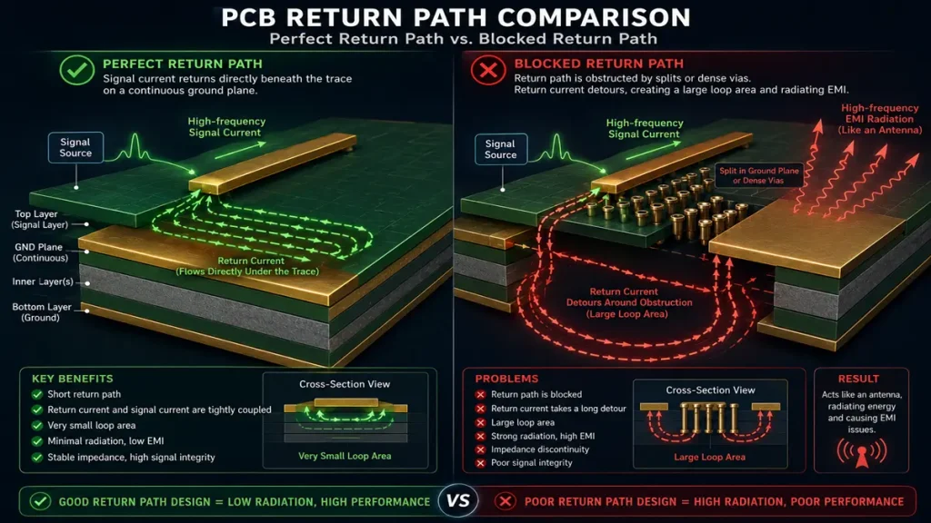
Figure 2: Geometrical quantization model of a honeycomb ventilation aperture array and its shielding effectiveness degradation boundaries under the IEC 61000-5-7 standard.
Stackup Architecture Optimization and 3D EDA Simulation Toolchains
Resolving backplane EMC failures requires a heavy reliance on high-fidelity 3D full-wave electromagnetic field simulation suites for pre-layout sweep analyses and post-layout verification. Industry regulations mandate the combined use of Ansys SIwave / HFSS, Cadence Sigrity Aurora, and Keysight ADS to perform co-extracted impedance calculations, common-mode scattering parameter extractions, and plane cavity resonance frequency sweeps. The core stackup and routing layout specification matrix is outlined below:
| Core Design Rules | Engineering Quantization Implementation Targets | Target Data Rates & Key Technical Objectives |
|---|---|---|
| Ultra-Narrow Power-GND Interlayer (Power-GND Proximity) | The physical dielectric spacing between the primary power plane and its adjacent main ground return layer must be tightly restricted to ≤ 2.0 mils (0.05mm). | Fully covers 56G, 112G, and 224G core PDN configurations. Ensures that power plane cavity high-frequency resonance peaks remain globally below -30 dB across the 10GHz–40GHz spectrum. |
| Zero-Split Return Plane Continuity (Plane Continuity) | Reference ground planes adjacent to ultra-high-speed routing layers must maintain 100% continuous, split-free copper within the signal trace projection zones. | Applicable to 112G and faster SerDes. The clearance boundary from the edges of via anti-pad clusters to differential trace edges must be maintained at > 3 × trace width. |
| Pure Internal Stripline Routing Mode | Routing high-speed traces on Top/Bottom surface layers is strictly prohibited. Ultra-high-speed channels must be encapsulated within internal striplines symmetrically sandwiched between dual ground planes. | Mandatory for 112G / 224G core physical paths. Leverages top/bottom solder masks and internal dielectric layers to form a native Faraday shielding cavity out of the copper ground planes. |
Extreme Physical Constraints on Intra-Pair Skew
When designing 224G PAM-4 ultra-high-speed physical links, the margin of error for intra-pair length matching shrinks to a brutal physical limit. According to the jitter and eye margin specifications outlined in the IEEE P802.3dj Draft Framework and OIF-CEI-224G-LR (Long Reach Interface Specifications), the dynamic intra-pair skew between the positive and negative complementary traces of a differential pair must be strictly limited to under 0.5 ps (which translates to an incredibly small absolute geometric length delta of ±2.5 mils on a Panasonic Megtron 7 dielectric laminate copper board). Once the skew exceeds a threshold of 0.8 ps, the common-mode reflection/transmission conversion parameter (SCD21) at the 56 GHz Nyquist frequency degrades immediately past -15 dB, turning regulatory radiated emission metrics red instantly.
Thermal vs. EMC Design: Shielding Effectiveness Compromises
Because the Thermal Design Power (TDP) of core ASICs on a single high-power line card routinely climbs above 250W–450W, backplanes and card cages must feature exceptionally dense airflow ventilation patterns. However, structural cutouts inherently compromise the chassis’s electromagnetic shielding integrity. For an isolated single vent hole, engineering practice generally dictates adhering to the classic Waveguide-Below-Cutoff design paradigm, where the maximum physical diameter of the aperture must be smaller than λ0 / 20:
Dsingle ≤ c / (2 × fmax × √(με)) ≈ λ0 / 20
For high-order electromagnetic bands extending up to 40 GHz–50 GHz, this means individual hole diameters must be capped below 3.5 mm. However, in actual systems, thermal architectures require high open-area ratios implemented via Perforated Aperture Arrays or Honeycomb Arrays. When a massive cluster of holes is arranged in an array, intense near-field EM coupling occurs between the apertures, causing the overall Shielding Effectiveness (SE) of the enclosure to severely degrade.
Pursuant to the quantitative modification specifications in international industrial standard IEC 61000-5-7 (Standard for Evaluation of Electromagnetic Shielding Performance of Enclosures), the total far-field shielding effectiveness of a dense perforated aperture array is governed by the following multi-aperture degradation formula:
SEarray = SEsingle – 20 × log10(n) + 20 × log10(λ0 / (2 × s))
Formula Application Boundary Conditions: This array calculation formula is strictly valid for sub-wavelength electro-small hole array regions where individual aperture diameters satisfy d < λ0 / 2 and center-to-center spacing satisfies s ≪ λ0. Here, n represents the total number of valid apertures falling within the primary illumination patch area of the radiation source, and s is the geometric center-to-center pitch of adjacent honeycomb cells.
Practical Deployment Guidance: When the total number of holes on a line card’s high-airflow bezel grid exceeds n > 400, the 20 log10(n) term inflicts a massive shielding degradation penalty of several tens of decibels. If the original 3.5mm aperture size is maintained, the enclosure’s attenuation performance performance beyond 30 GHz collapses completely. Consequently, engineering teams must micro-scale the honeycomb cell diameter down to ≤ 1.5 mm, while simultaneously ensuring that the geometric depth of the metal grid wall is at least 3 times the cell diameter. This establishes a cutoff waveguide array with high attenuation density, ensuring that the entire chassis maintains an empirically verified shielding effectiveness of greater than 35 dB up into the 40 GHz high-frequency band.
VI. Complete Closed-Loop EMC Troubleshooting Flowchart
                                  [ COMPLIANCE FAILURE DETECTED ]
                                                 |
                        +------------------------+------------------------+
                        |                                                 |
                [ Radiated Emissions ]                          [ Conducted Emissions ]
                        |                                                 |
            Is noise narrow or broadband?                     Check PDN Switching Noise
                        |                                                 |
        +---------------+---------------+                     Inspect VNA Impedance Profile
        |                               |                     from 100 kHz to 10 GHz
   [Narrowband]                    [Broadband]                            |
        |                               |                      Are resonant peaks > Target?
  Check Clock Traces,             Check Differential Pair                 |
  Crystal Shielding &             Intra-pair Skew (>0.5ps)         +------+------+
  Enclosure Slit Ratios                 |                          |             |
        |                         Is Skew Balanced?               [Yes]         [No]
  Fix Apertures &                  +----+----+                      |             |
  Add Stitching Vias               |         |             Optimize Decoupling    Inspect Ferrite
  (<λ/20 spacing)              [Yes]     [No]           Capacitor ESR Matrix   Bead Transient
        |                          |         |             & Stackup Thickness    Ringing
[RE-TEST COMPLIANCE]      Check Connector  Re-route to                     |             |
        ^                 Ground Ratios    Fix Skew                  Add Plane    Bypass/Reduce
        |                 & Plane Splits     Path                     Cavity Damp   Ferrite Value
        +-----------------------+------------+-----------------------------+-------------+
VII. In-Depth Case Studies of Real-World Industrial High-Speed Backplane EMC Failures
Case A: Optimization of Ultra-High-Frequency Radiation Leakage in a 400GbE Data Center Core Switch Backplane
System Fundamental Physical Parameters: Implemented on a 28-layer ultra-high-density backplane, constructed out of Panasonic Megtron 7 class ultra-low-loss dielectric laminates, featuring a total board thickness of roughly 4.5 mm. Signal layers feature a copper weight of 1/2 oz, and high-frequency power/ground core interlayer spacing is configured at 2.5 mils.
Quantitative Compliance Testing Data: The system passed completely with green lights across the default testing spectrum below 6 GHz when evaluated under the CISPR 32 Class B regulatory framework in a commercial laboratory. However, given that it houses a 112G PAM-4 interconnect bus operating at blinding speeds, the design team extended the scan frequency upward according to FCC guidelines to proactively safeguard against near-field secondary resonances degrading the noise floor. When scanning up into the 28.1 GHz high-frequency band, the EMI receiver captured an anomalously sharp, soaring radiation peak peaking at 54.8 dBμV/m, overshooting the extrapolated regulatory limit line by a massive +11.4 dBμV/m. The diagnostic instrument setup utilized a Tektronix DPO75002SX 50GHz high-bandwidth real-time oscilloscope alongside an R&S ESW44 high-end EMI test receiver.
3D Field-Level Root Cause Diagnosis: The R&D team sliced and imported the board’s physical CAD model into Ansys HFSS to perform 3D full-wave finite element electromagnetic field simulation extractions. The results locked the failure source dead to the high-speed connector press-fit via field area at the daughter card-to-backplane mating boundary. The system utilized an early, unoptimized binary-weighted DAC driver lacking integrated full shielding encapsulation, generating up to 18.2 mV of high-frequency residual common-mode potential. More critically, this via field selected an outdated backplane connector whose internal pin mapping enforced a ground-to-signal pin ratio of merely 1:1. Consequently, when signal vias transitioned layers at Layer 14, their high-frequency return paths were cleanly truncated by widespread anti-pad voids, forcing the return currents to detour around to edge stitching vias located over 4.0mm away, thereby driving intense spatial dipole field radiation.
Closed-Loop Engineering Remediations: 1. Software-side reconfiguration of the SerDes driver registers to toggle active thermometer-coded DAC algorithms that boast native phase symmetry, suppressing dynamic P/N phase imbalance down below 0.4 ps right at the silicon core source; 2. Scrapped the legacy connector in favor of the industry-benchmark Amphenol Paladin high-speed backplane connector series and re-architected the via field array to enforce a strict 2:1 ground-to-signal pin ratio (GND-to-Signal Pin Ratio). In this upgraded array configuration, every high-speed differential pin pair is completely surrounded by native solid metal ground shielding pins, forming a “Faraday Cage” isolation perimeter. Following these modifications, a high-frequency re-test was conducted in the lab; the RF radiation spike at 28.1 GHz plummeted by 15.3 dB, cleanly securing market compliance authorization.
Case B: Broadband Noise Violation Sparked by Reference Plane Splits Crossing in a Large Telecom Chassis Switch Backplane
System Fundamental Physical Parameters: A 32-layer large-scale Central Office central switch fabric backplane fabricated out of Nelco N4000-13 SI high-performance dielectric material (εr ≈ 3.4), running multiple concurrent 56G NRZ core SerDes links.
Quantitative Compliance Testing Data: During FCC Part 15 Subpart B Class A compliance radiation scanning, empirical data revealed a massive, rolling broadband electromagnetic emission breach spanning the ultra-high-frequency band from 14 GHz to 22 GHz, with a peak radiation emission topping out at 54.2 dBμV/m. According to 47 CFR §15.33 statutory mandates regarding high-frequency detection boundaries for unintentional radiators: the upper frequency limit must extend to the 5th harmonic of the highest operating clock frequency or reach 40 GHz, whichever is lower (capping this system’s test suite precisely at 40 GHz). This broad noise envelope clearly breached the Class A red line near 20 GHz, constituting a definitive compliance failure.
Time/Frequency Domain Impedance Tracking & Physical Source Extraction: Debugging personnel deployed a Keysight N1000A DCA-X sampling oscilloscope equipped with a TDR module to perform a dragnet sweep across the failing channels. Measurements revealed that on internal routing Layer 18, the trace impedance suddenly spiked to 145 ohms. Cross-checking the layout artwork uncovered that a layout designer had carved out a 50-mil-wide isolated moat on the Layer 19 adjacent reference ground. 12 channels of serial 56G NRZ data trunks crossed directly over this isolation moat, inducing a total collapse of their high-frequency return paths.
The deep physical explanation for why the broadband noise emission concentrated precisely around 18.5 GHz lies in the excitation of a high-Q power-ground interlayer metal cavity resonance within the massive backplane. The layout split formed an ungrounded rectangular cavity region measuring L = 10.5 mm by W = 8.1 mm within the Nelco dielectric substrate (εr ≈ 3.4 fixed). In accordance with multi-mode electromagnetic cavity propagation equations, while the fundamental TE10 wave initiates at a much lower boundary (~7.75 GHz), the high-speed SerDes non-linear harmonics dynamically drove a higher-order hybrid TE21 cavity mode. Calculating the physical resonant boundary condition for this specific high-order hybrid mode confirms:
f21 = [ c / (2 × √εr) ] × √[ (2/L)2 + (1/W)2 ] ≈ [ 3×10⁸ / (2 × √3.4) ] × √[ (2/0.0105)2 + (1/0.0081)2 ] ≈ 18.46 GHz
This match shows that the TE21 high-order hybrid cavity mode peak sat precisely at **18.46 GHz**, aggressively acting as a tuning fork that amplified the common-mode energy bridging the ground split and creating massive broadband radiation leakage.
Closed-Loop Engineering Remediations: 1. In the subsequent PCB spin, all 12 pairs of ultra-high-speed links were mandatorily migrated to secure internal Layer 12 stripline configurations, ensuring that their upper and lower sandwich interfaces run over 100% solid, un-split reference ground layers; 2. Adopted the premium Molex Impel+ ultra-high-speed backplane connector architecture to establish a hyper-compact via return field, completely decoupling signal boundaries from structural components via the connector’s internal leaf-style full-shielding metal shrouds; 3. Added surface-mount, low-ESR, low-ESL 0201-packaged 0.1 μF high-frequency AC stitching capacitors bridging both non-critical DC power rails flanking the isolation moat. This provided an immediate local AC shunting pathway to ground out any residual common-mode electromagnetic resonances. Following these remedies, the overall broadband EMI noise envelope collapsed below 38.5 dBμV/m, successfully reclaiming a robust compliance safety margin of up to 9.5 dB.
Expert FAQ: Key Quantitative Answers to High-Speed Backplane EMC Challenges
In 112G/224G transmission systems, what is the most critical S-parameter metric for assessing PCB differential-to-common mode leakage?
The primary quantitative benchmark is the **differential-to-common mode conversion parameter (SCD21 or SCD11)**. In full-wave EM simulations, if a 224G differential routing channel exhibits an SCD21 that degrades past the golden threshold of **-20 dB** at the 28 GHz or 56 GHz Nyquist frequency points due to via stubs or line asymmetries, it indicates that over 10% of the high-frequency differential signal energy is being physically degraded and converted into common-mode energy. This almost guaranteed predicts an immediate failure during physical FCC radiated emission tests downstream.
When designing layer-transitions for mainstream ultra-high-speed backplane connectors like Amphenol Paladin or Molex Impel+, are there hard quantitative metrics for the pin grounding ratio?
In backplane configurations pushing single-lane rates up to 112G/224G PAM-4, legacy 1:1 ground-to-signal ratios are completely obsolete. Standard industry blueprints (such as the Amphenol Paladin or Molex Impel+ series) mandate implementing a **ground-to-signal pin ratio of ≥ 2:1** across the connector footprint layout. This dictates that every pair of high-frequency differential signal pins must be completely boxed in on its top, bottom, left, and right boundaries by dedicated solid ground shielding pins, guaranteeing that spatial electromagnetic fields maintain the shortest physical return current loops when routing through connector split interfaces, thereby compressing via cross-talk and field leakage to the absolute minimum.
When simulating and evaluating ultra-fast SerDes driver edge rates below 20ps, how should one scientifically select the fmax formula in pre-layout simulation setups?
When a silicon block’s rise time shrinks to t_r ≤ 20 ps and exhibits clear substrate non-linear compression or ringing, you must completely abandon conservative fmax = 0.5/t_r approaches. You must mandatorily deploy **fmax = 1/(π × t_r)**. This formula properly pushes the computational domain bandwidth up to the 5th harmonic envelope edge past 50 GHz, enabling 3D HFSS models to accurately extract parasitic side-lobes of via stubs and high-order cavity resonances, avoiding late-stage lab RE compliance busts caused by blind-spots in simulation bandwidth.
Can adding board-level shielding cages or metallic chassis meshes effectively patch up EMC radiation triggered internally by severed return current paths?
**Absolutely not.** This is a classic engineering misconception. Shielding cages can only block near-field capacitive E-field radiation propagating directly through the air. Once high-frequency return paths encounter slot-level discontinuities, common-mode currents diffuse rapidly through internal copper conductive layers, grounding standoffs, and the power distribution network (PDN). This “conducted common-mode noise” will easily flow around internal shielding enclosures, tracking along low-speed ribbon cables or external I/O wires straight outside the chassis shield, generating massive system-level regulatory radiation failures.
Why do some chassis assemblies demonstrate generous EMC margins in lower bands below 6 GHz, yet suddenly encounter massive radiation violations across the 18 GHz–40 GHz spectrum?
This anomaly is typically driven by slot-length resonances between structural metal housing seams and floating board-level heatsinks. For a 40 GHz electromagnetic wave, its wavelength in air is a mere 7.5 mm, compressing its 1/2 wavelength resonant physical dimension down to 3.75 mm. This means that if any continuous, non-conductive gaps exceeding 3.5mm exist along the front panel module seams, pull-tabs, or fan tray finger gaskets, that seam will trigger aggressive slot-antenna resonance under high-frequency exposure. Additionally, large aluminum alloy heatsinks mounted over high-power ASICs will transform into floating patch antennas if they are not solidly anchored to ground via ultra-dense ground grounding fingers (anchoring pitch typically required to be < 15 mm), driven dynamically by stray fields escaping the IC die and spraying out intense RF energy.
IX. Conclusion and Systemic Actionable Recommendations for R&D Engineering
High-speed backplane EMC design is a highly quantitative, interdisciplinary science governed by strict physical boundary constraints. Faced with a non-compliant substrate assembly, engineering remediation should follow this “Cost-to-Effectiveness” priority matrix to systematically drive self-audits and architectural re-spins:
- Priority 1: Firmware-Side SerDes Active Compensation Tuning (Cost: Zero / Time-to-Benefit: Instant)
Before committing to a high-cost PCB re-spin or mechanical tooling modifications, collaborate with your silicon vendor’s physical layer engineering team to modify low-level firmware registers and engage the chip’s internal Active Skew Compensation engines. Finely tune the SerDes channel output slew rates and force the high-speed transmitter blocks into highly symmetric thermometer-coded DAC modes, neutralizing up to 10dB+ of native common-mode fluctuation energy right at the silicon die level. - Priority 2: Return Path Topology Corrections and AC Slot Bridging (Cost: Extremely Low / Time-to-Benefit: Substantial)
Leverage automated Design Rule Checkers (DRC) via *Cadence Sigrity* or *Ansys SIwave* to perform a dragnet sweep of return paths across all 112G/224G core signal layers. If local cross-splits caused by power plane isolation moats or dense via anti-pads are discovered and routing paths cannot be re-routed, mount ultra-low ESR 0201 impedance-matched AC stitching capacitors tightly flanking the projection margins of the split signal traces. This forces return loops to contract without needing a total layer re-route. - Priority 3: Enclosure Seam Scaling and Airflow Vent Honeycomb Re-tooling (Cost: Moderate / Time-to-Benefit: Comprehensive)
Re-verify system fan ventilation grids in strict accordance with IEC 61000-5-7 multi-aperture array degradation laws. Completely phase out open vent patterns with single slots exceeding 3.5mm, upgrading fully to dense honeycomb perforated grids characterized by cell diameters of ≤ 1.5 mm and a high depth-to-width ratio. Simultaneously, line the mating junctions where daughter boards slot into backplanes with dense conductive foam or beryllium copper gaskets to mechanically break up all unshielded structural seams down below 2.0 mm. - Priority 4: Full Stackup Re-Architecture and Connector Overhauls (Cost: High / Time-to-Benefit: Absolute)
If all preceding firmware and surface modifications fail to drag the emission profiles back under the compliance limit lines, it indicates a systemic collapse of the board’s internal EM confinement. You must deploy a fundamental architectural re-design: sink all channels exceeding 56G entirely into internal stripline layers; compress power/ground core dielectric interlayers tightly to ≤ 2.0 mils; and fully swap out all mating interface via connectors with high-performance multi-gigabit shielded connectors boasting ground-pin ratios of 2:1 or higher, such as the Amphenol Paladin or Molex Impel+ series.
Baseline Engineering Consensus: In 112G / 224G high-speed datacom hardware development, EMC compliance can never be successfully patched late in the cycle by haphazardly soldering capacitors or stringing ferrite beads. It must be an integrated, closed-loop simulation pipeline that starts with active silicon driver symmetry, flows through 100% continuous PCB return path topography, and culminates within a waveguide-below-cutoff micro-perforated structural enclosure.
X. Standardized Engineering References
- Federal Communications Commission (FCC), “Title 47 of the Code of Federal Regulations (CFR) – Part 15 Radio Frequency Devices – Subpart B: Unintentional Radiators – Section 15.33 Frequency range of radiated measurements,” Washington D.C., 2025.
- International Special Committee on Radio Interference (CISPR), “CISPR 32: Electromagnetic compatibility of multimedia equipment – Emission requirements,” Ed. 2.1, Geneva, 2023.
- International Electrotechnical Commission (IEC), “IEC 61000-5-7: Electromagnetic compatibility (EMC) – Part 5-7: Installation and mitigation guidelines – Degrees of protection provided by enclosures against electromagnetic disturbances (EM code),” Geneva, 2016.
- IEEE P802.3dj, “Draft Standard for Ethernet Amendment: Physical Layer Specifications and Management Parameters for 200 Gb/s, 400 Gb/s, 800 Gb/s, and 1.6 Tb/s Operation Using 224 Gb/s Signaling,” IEEE Draft 2.0, February 2026.
- Optical Internetworking Forum (OIF), “Implementation Agreement for Common Electrical I/O (CEI) 224G-LR Implementation Agreement Project,” OIF-CEI-224G-LR-01.0, November 2025.
- C. Hwang, Y. J. Zhang, and D. Pommerenke, “Mitigation of Differential-to-Common Mode Conversion in High-Speed SerDes Differential Channels via Structural Balancing,” IEEE Transactions on Electromagnetic Compatibility, vol. 62, no. 4, pp. 1245-1256, Aug. 2020.
- H. Heck, M. R. Selli, and T. G. R. S. Consortia, “High-Speed Interconnect Optimization and Radiated Emissions Risk Analysis for 112G/224G PAM-4 Channels,” in Proc. IEEE International Symposium on Electromagnetic Compatibility & Signal/Power Integrity (EMC+SIPI), pp. 312-318, July 2024.
Using top-tier AI server PCB equipment to manufacture traditional PCBs delivers a strategic advantage: interlayer alignment tolerance shrinks from ±75μm to within ±25μm, and differential impedance control tightens to ±5%. Paired with 100% 3D X-Ray inspection, it grants conventional boards chip-level precision, superb signal stability, and near-100% yield.
Still, need help? Contact Us: sales@pcbkr.com
Need a PCB or PCBA quote? Quote now
About Author
David Chen https://www.linkedin.com/in/pcbcoming
David Chen boasts an extensive professional background in PCBA manufacturing, PCBA testing, and PCBA optimization, with specialized expertise in high-precision PCBA fault analysis and rigorous PCBA reliability testing. The author has worked with high-layer-count server PCB fabrication, ultra-low-loss backplane stackups, and thermo-mechanical reliability optimization for AI infrastructure projects involving 112G and 224G PAM4 architectures. Skilled in complex circuit design and cutting-edge advanced PCB manufacturing processes, he delivers solutions that elevate product durability and performance across industrial applications. His technical articles focusing on PCBA manufacturing workflows and testing methodologies are widely cited by industry peers, research institutions, and technical platforms, solidifying his reputation as a recognized technical authority in the global circuit board manufacturing sector.