Why AI Backplane & UBB PCBs Are Far More Complex Than Traditional Backplanes
Technical Whitepaper & Advanced Manufacturing Deep Dive
Why AI Backplane & Universal Baseboard (UBB) PCBs Are Far More Complex?
AI Backplane & Universal Baseboard (UBB) PCBs – High-Speed AI Infrastructure Solutions by PCBKR
The complexity surge stems from the transition from 25G/56G NRZ to 112G/224G PAM4 signaling. This architectural shift compresses the total end-to-end channel insertion loss budget to a critical ~28–32 dB at 56 GHz (including silicon package and module losses). It forces hardware infrastructures to transition away from traditional long-distance copper-embedded routing toward hybrid topologies featuring high-density Overpass Twinax Cables, Orthogonal Direct-Mate connectors, and Co-Packaged Optics (CPO).
Traditional Backplane PCB Architecture (25G / 56G Era)
Direct Summary: Legacy enterprise backplanes rely entirely on inner-layer copper traces within multi-layer PCBs to route signals between disparate line cards. At signaling rates up to 56 Gbps PAM4, the system easily tolerates predictable dielectric attenuation and moderate connector impedance discontinuities without requiring external bypass mechanisms.
In traditional telecom and enterprise server chassis operating at 25 Gbps NRZ, the Nyquist frequency is locked at 12.5 GHz. In this spectrum, standard low-loss laminates (e.g., Panasonic Megtron 6) present a mild dissipation factor (D_f) of approximately 0.002 at 12.5 GHz. Signals traverse long, embedded copper traces up to 500 mm (approx. 20 inches). With total channel loss budgets accommodating 35 to 40 dB, engineering margins remain highly forgiving.
Engineering teams designing these large-format backplanes (typically 600 mm × 450 mm, 16 to 24 layers) utilize standard via structures. Controlled-depth backdrilling is sufficient if it keeps the remaining via stub below 0.20 mm. At 12.5 GHz or even 28 GHz, a 0.20 mm stub places the quarter-wave resonant notch frequency near 187 GHz—far outside the operating band. Mechanical connector insertion loss stays under 1.0 dB, and the wide eye-opening of NRZ modulation comfortably tolerates impedance deviations up to ±10% while easily maintaining a strict Bit Error Rate (BER) target of 1 × 10^{-12}.
AI Clusters & Universal Baseboard Requirements (112G / 224G PAM4 Era)
Next-generation 112G and 224G PAM4 architectures redefine electrical layout rules. Because PAM4 signals compress voltage margins to one-third of NRZ, the maximum allowable PCB-only trace loss is capped at ~12–15 dB of the total channel budget. This restricts maximum pure copper routing distances on the Universal Baseboard (UBB) to under 120 mm, mandating structural evolution toward hybrid layouts.
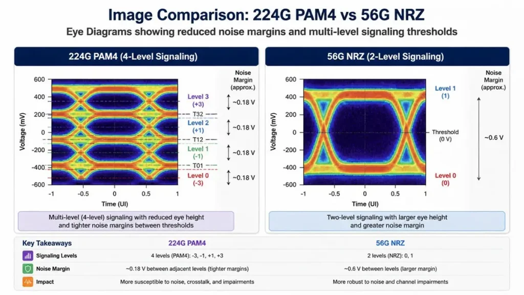
224G PAM4 vs. 56G NRZ Eye Diagram Analysis and Signal Integrity Comparison (Simulated by PCBKR Lab)
As clusters advance into the 224 Gbps PAM4 domain, the Nyquist frequency climbs to 56 GHz. At this frequency, inner-layer trace attenuation on legacy low-loss substrates spikes past 3.5 dB per inch. To ensure compliance, modern AI Accelerator Universal Baseboards (UBBs) and high-speed Switch Fabrics constrain maximum on-board copper routing to a strict 120 mm ceiling. High-frequency channels must exit the lossy PCB dielectric as quickly as possible.
[Switch/GPU ASIC] ──(Short PCB Trace < 5″) ──> [Overpass Connector] ──(Twinax Cable) ──> [I/O Module / Switch Fabric]
Simultaneously, thermal density and power distribution requirements expand exponentially. In next-generation AI accelerator platforms packing 8 to 16 OAMs (Open Accelerator Modules), a single GPU ASIC’s localized thermal dissipation exceeds 700W to 1000W. Structurally, the supporting UBB must handle extreme layer counts (28 to 44+ layers) and withstand continuous localized operating temperatures over 180°C (T_g). Under intense thermal expansion stresses, the substrate must maintain absolute mechanical flatness to prevent microvia fatigue and structural fracturing.
Signal Integrity Challenges at 112G/224G
Routing 56 GHz Nyquist channels exposes signals to extreme skin effect attenuation, copper surface roughness losses, destructive via-stub resonance, and glass fiber-weave skew. Failing to manage substrate material uniformity and via geometries at a micron scale results in immediate, catastrophic closure of the 224G PAM4 eye diagram.
1. Skin Effect and Copper Roughness Loss: At 56 GHz, the skin depth of copper drops below 0.28 μm. If the copper foil surface roughness profile (R_z) exceeds 1.5 μm, the high-frequency current is forced to follow the jagged microscopic valleys of the foil. This artificially extends the transmission path length, driving conductor losses up by more than 40%.
2. Resonant Via Stubs: In a 224G link, any remaining un-backdrilled via stub exceeding 0.05 mm (2 mils) acts as an open-ended stub resonator. This introduces a steep, destructive resonance notch near the 56 GHz operating frequency, completely devastating channel Return Loss and violating compliance boundaries (< -8 dB).
3. Fiber-Weave Skew: Standard E-glass fabrics contain highly non-uniform glass bundles (high permittivity, ε_r ≈ 6.0) separated by resin-rich windows (low permittivity, ε_r ≈ 3.0). When differential signal pairs run asymmetrical to these weave patterns, a phase velocity mismatch occurs. This yields over 15 picoseconds (ps) of intra-pair skew over short lengths, transforming vital differential signals into destructive common-mode noise.
Transition from PCB Traces to Hybrid Interconnects
To bypass the physical limitations of 56 GHz copper routing, system architects bypass internal long-distance PCB routing. Instead, they extract signals via tight microstrips directly into Overpass Twinax cable assemblies or adopt Orthogonal Direct-Mate architectures to interface line cards with switch cards directly.
Twinax Cable Integration & Orthogonal Architectures
In modern AI switch configurations, high-frequency signals no longer travel across 400 mm of internal resin substrate. Signals route from the ASIC pads through a short microstrip trace (<50 mm) directly to an automated, surface-mounted vertical connector launcher. From there, they jump into highly shielded, silver-plated copper Twinax cables. Exhibiting a remarkably low loss profile of roughly ~0.35 dB/inch at 56 GHz, these assemblies completely isolate the channel from the lossy PCB core.
Concurrently, Orthogonal Direct-Mate architectures eliminate midplanes entirely. Processing cards align at 90 degrees relative to switch fabrics, engaging directly through ultra-precise mechanical connectors. This point-to-point interface eliminates intermediate PCB trace routing, optimizes impedance continuity, minimizes single-point insertion loss to under 0.6 dB, and maximizes thermal dissipation efficiency by opening optimal airflow paths.
Overpass Cable (OPC): Bypassing the Backplane
Overpass Cable (OPC) is a structural topology that routes high-speed signals over the PCB surface using dedicated, air-spaced twinaxial ribbon cable assemblies, liberating critical paths from the dielectric loss inherent to multi-layer substrates.
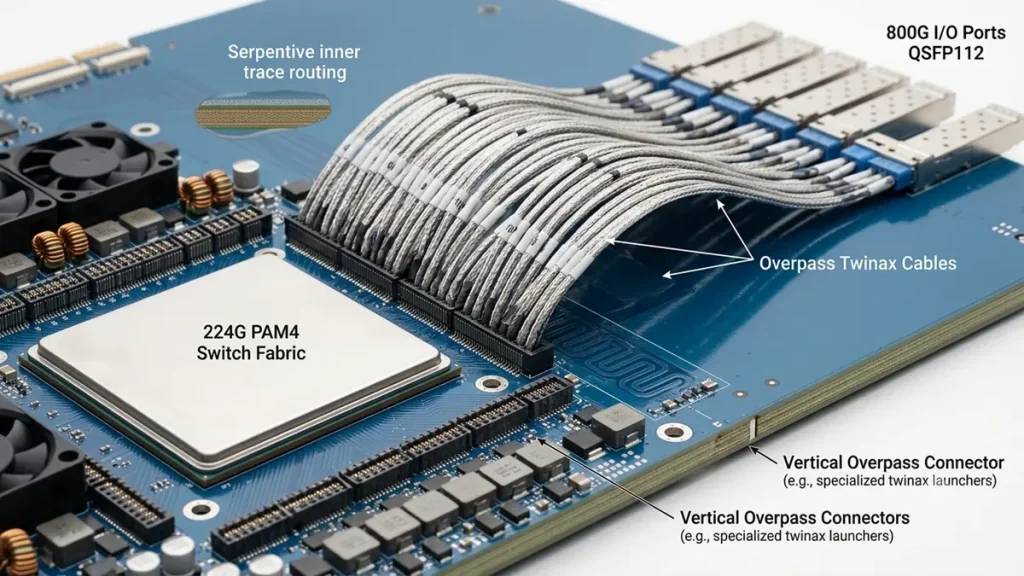
3D Architectural Detail of an Overpass Twinax Cable Assembly Terminating at the Perimeter of a 224G PAM4 Switch Fabric (Fabricated by PCBKR)
By positioning high-density Twinax footprints directly adjacent to the escape boundaries of high-performance Switch ASICs or High-Bandwidth Memory (HBM) packages, signals leave the silicon environment and transition instantly into air-cooled, individually shielded wire groups.
Quantifiable Advantage: Spanning a 400 mm trace routing domain using ultra-low-loss laminates (e.g., Megtron 7) generates an unacceptable dielectric insertion loss of over 45 dB. Incorporating an OPC setup clamps total channel insertion loss down to a highly compliant 14 dB. This optimization prevents the need to upgrade massive, 40-layer system mainboards entirely to cost-prohibitive specialty RF laminates, yielding a balanced overall Bill of Materials (BOM).
Manufacturing Challenges: Deploying OPC requires meticulous mechanical engineering and production assembly. Routing up to 128 differential pairs within a congested processor perimeter creates acute space constraints. This congestion can restrict local fan airflow and complicates automated SMT component placement, making post-assembly field maintenance more complex.
CPO (Co-Packaged Optics): Eliminating Electrical Bottlenecks
Co-Packaged Optics (CPO) removes the electrical copper bottleneck by mounting optical transceiver engines alongside the core ASIC switch within a single high-precision substrate, swapping out long-distance copper links for zero-loss optical paths.
Under a CPO architecture, high-frequency electrical interconnects are reduced to an absolute minimum—spanning a tiny 10 mm to 25 mm link between the ASIC SerDes pins and the optical engine. This micro-routing is fully contained within the controlled environment of the advanced multi-chip module substrate. From that point forward, data transfer across the AI cluster infrastructure travels via fiber optic lines. Because optical fibers are naturally immune to dielectric attenuation, cross-talk, and EMI at 56 GHz, standard PCB layout bottlenecks are avoided along the primary link.
However, CPO transfers structural challenges into electro-thermal co-design and ultra-dense microvia fabrication. Operating adjacent to optical modules, the ASIC core generates intense localized heat fluxes exceeding 15W/cm². Because laser sources are thermally sensitive—requiring tight stabilization below 70°C to prevent accelerated aging and wavelength drift—the host PCB must incorporate heavy embedded copper coins and matrixed thermal blind via arrays placed precisely beneath the optical engine footprints, pushing mechanical registration to manufacturing limits.
Materials and Stackup Complexity in AI PCBs
AI-tier substrates demonstrate unprecedented stackup complexity, typically featuring 28 to 44+ layers arranged in complex hybrid configurations. These stackups combine hyper-expensive ultra-low-loss resin matrices with specialized, flat-spread glass fabrics and ultra-smooth copper foils.
To highlight the engineering differences between legacy backplanes and next-generation AI hardware, the primary physical and electrical properties are detailed below:
| Process & Electrical Parameters | Traditional Enterprise Backplane (25G/56G Era) | AI Cluster Mainboard / UBB (112G/224G PAM4 Era) |
|---|---|---|
| Layer Count | 16 – 24 layers | 28 – 44+ layers ultra-high density |
| Core Substrate Materials | Panasonic Megtron 6 or industry-standard low-loss equivalents | Panasonic Megtron 7G / Megtron 8, Isola Tachyon 100G, TerraGreen |
| Dielectric Constant (D_k @ 56 GHz) | 3.6 – 3.9 | 3.0 – 3.2 hyper-low permittivity formulations |
| Dissipation Factor (D_f @ 56 GHz) | 0.002 – 0.004 | 0.0010 – 0.0012 ultra-low loss spectrum |
| Copper Foil Classification | RTF (Reverse Treated Foil) or standard Low-Profile | HVLP (Hyper Layer Low Profile) / Ultra-HVLP (R_z \le 1.0\,\mu\text{m}) |
| Glass Fabric Configuration | Standard 1080 / 2116 E-Glass woven structure | Mechanically spread, ultra- flat flat-glass styles (e.g., 1078 / 1067 styles) |
To eliminate fiber-weave skew, modern AI boards mandate mechanically flat-spread glass styles (such as 1078 or 1035). In these configurations, glass bundles are flattened during weaving to eliminate resin-rich windows. In hybrid stackup topologies, to optimize overall material cost, engineers route critical 56 GHz channels exclusively on high-grade outer or selected inner layers using Megtron 8, while interleaving standard high-T_g FR-4 materials for internal power and ground planes. This requires precise internal stress balancing during the multi-stage lamination cycles.
Manufacturing Challenges & Process Tolerances
On the fabrication floor, AI high-layer substrates encounter demanding yield constraints: including a strict ±5% characteristic impedance uniformity window, material registration shift across up to 44 layers, and ultra-deep controlled backdrilling requirements.
[Layer 01] ══════════════ (Top Trace) [Layer 02] ══════════════ [Layer 03] ══════ ══════ (Target Signal Trace Layer) ║ │ ║ │ <– Precision Backdrill Bit (Removes copper barrel) ║ ▼ [Layer 40] ╚═════════════ (Target Depth Point: Remaining Stub MUST be < 0.05mm)
1. Layer-to-Layer Registration Control: In a dense, 4.0 mm thick substrate spanning more than 40 layers, material expansion and contraction during high-temperature lamination cycles induces micro-scale shifting of internal pad centers. To guarantee that a 0.25 mm drill bit cleanly clears 0.40 mm pitch via configurations without causing internal shorts, manufacturing centers utilize pinless induction bonding systems matched with pre-lamination real-time X-ray expansion scaling, keeping registration errors strictly \le 35\,\mu\text{m}.
2. Deep Controlled-Depth Backdrilling: Drilling through a thick 4.0 mm substrate with a 0.25 mm micro-drill to eliminate a via barrel down to Layer 3 while maintaining a residual stub under 0.05 mm (2 mils) requires exceptional precision. Due to natural micro-warpage across large panel surfaces, basic depth-calculated drilling causes high failure rates—either leaving extended stubs that introduce resonant notches or over-drilling and destroying internal signal lines. Fabricators address this by integrating closed-loop Z-axis electrical contact sensing feedback to calculate absolute zero the moment the bit touches the panel surface.
3. Ultra-HVLP Copper Delamination Mitigation: To maximize signal integrity, Ultra-HVLP copper foil profiles minimize roughness (R_z \le 0.8\,\mu\text{m}), which reduces mechanical bonding area and peel strength. Throughout subsequent lead-free reflow profile cycles peaking at 288°C, internal stresses can trigger delamination along smooth copper interfaces. Production lines counteract this by applying organo-silane adhesion promoters to modify the copper surface chemically at a molecular level, establishing strong adhesion without altering smooth surface profiles.
Engineering Insight: Real-World Layout and Manufacturing Lessons
“When laying out channels for 224G PAM4 links, treating a PCB trace as a basic copper wire will lead to severe signal degradation. At 56 GHz, every feature, split-plane transition, and via antipad functions as an active RF circuit component.
In a recent 800G switch fabric project, the initial prototype experienced high packet drop rates during full-load qualification. Our internal SI team diagnosed the board using 3D full-wave electromagnetic field solvers. The root cause traced back to standard oval antipad configurations used around high-speed differential vias. This geometry introduced excessive parasitic capacitance, dropping localized characteristic impedance to 82 Ω and causing severe reflections.
To resolve this for the specific stackup configuration, we modified the structure to a customized 1.2 mm circular ground-shielded antipad. On the production floor, we implemented automated Time-Domain Reflectometry (TDR) inline screening at a strict ±5% tolerance window. This modification pulled the impedance discontinuity back to a compliant 95 Ω, stabilized return loss, and eliminated packet loss. In high-frequency designs, structural simulation must be tightly coupled with manufacturing process controls.”
—— Principal Systems Architect, Shenzhen Hongda Circuit Technology Co., Ltd. (PCBKR)
Our manufacturing base in Shenzhen, China (Shenzhen Hongda Circuit Technology Co., Ltd. / PCBKR) specializes in high-speed, high-frequency fabrication. By combining automated optical inspection (AOI), precise Z-axis contact backdrilling systems, and extensive experience with advanced substrates like Megtron 8 and Tachyon 100G, we ensure every AI server substrate and high-speed backplane meets stringent industrial requirements.
FAQ: Advanced Interconnect & Fabrication Deep Dive
Why do 224G PAM4 channels enforce strict trace length limits compared to 25G NRZ?
This restriction is driven by dielectric insertion loss and skin effect attenuation at high frequencies. A 224G PAM4 signal runs at a 56 GHz Nyquist frequency, where attenuation can exceed 3.5 dB per inch even on advanced substrates. Because PAM4 utilizes multi-level signaling with reduced noise margins, the total allowable board-level trace loss is capped around 12–15 dB. Restricting copper trace runs to under 120 mm prevents total eye closure. Conversely, 25G NRZ operates at 12.5 GHz, where dielectric attenuation is much lower, permitting trace lengths over 500 mm within a broader 35 dB channel budget.
How does Overpass Cable (OPC) technology improve insertion loss characteristics inside AI architectures?
OPC routing bypasses lossy PCB core dielectrics. By surface-mounting high-density twinaxial connectors close to the ASIC escape boundaries, high-frequency signals transition directly into air-spaced, shielded twinaxial cable assemblies. Twinax cables exhibit an insertion loss of only ~0.35 dB/inch at 56 GHz. This drops the total attenuation across a 400 mm link from an unacceptable 45 dB down to a compliant 14 dB, ensuring signal integrity without requiring the entire multi-layer board to be fabricated from specialty RF substrates.
What is fiber-weave skew, and how is it managed during AI PCB fabrication?
Fiber-weave skew occurs when differential trace pairs cross standard woven glass styles asymmetrically. The dielectric constant varies between the dense glass bundles (D_k ~6.0) and resin-rich interstitial windows (D_k ~3.0). At 56 GHz, this non-uniformity introduces intra-pair propagation delay skew exceeding 15 ps over short distances, causing phase misalignment and converting differential signals into common-mode noise. Fabricators manage this by specifying mechanically flat-spread glass styles (e.g., 1078/1067), which flatten glass fibers to eliminate resin windows, or by routing differential pairs at an angle (10° to 45°) relative to the glass weave axis.
What mechanical risks do Ultra-HVLP copper foils present during lead-free reflow, and how are they mitigated?
Ultra-HVLP copper foils feature an ultra-smooth profile (R_z ≤ 1.0 μm) to minimize skin effect losses. However, this smooth surface reduces mechanical interlocking friction with the resin substrate, lowering peel strength. During lead-free reflow cycles peaking near 288°C, mismatched coefficients of thermal expansion (CTE) generate internal shear stresses that can cause delamination or blistering. Fabricators mitigate this risk by applying organo-silane adhesion promoters post-etching, chemically treating the smooth copper surface to enhance bonding without increasing surface roughness.
Why does 224G PAM4 routing require specialized backdrilling controls compared to standard controlled-depth methods?
Standard backdrilling relies on calculated mechanical Z-axis depth limits, typically leaving residual via stubs between 0.15 mm and 0.25 mm. At a 56 GHz Nyquist frequency, a 0.20 mm stub acts as a quarter-wave resonator, creating a sharp resonance notch that disrupts channel return loss. To meet the strict ≤0.05 mm (2 mils) stub limit required for 224G signaling, fabricators use automated backdrilling systems equipped with closed-loop electrical contact sensing. The drill detects the exact moment it touches the internal copper layer, establishing a precise zero-point that compensates for panel warpage.
Find Out About Us: Delivering Top-Tier Fabrication for Both AI & Conventional PCBs
Navigating the line between cutting-edge innovation and high-volume, cost-effective production shouldn’t be a compromise. At Shenzhen Hongda Circuit Technology (PCBKR), we bridge this gap by elevating the manufacturing standards for both high-performance AI hardware and traditional multi-layer PCBs.
By integrating advanced manufacturing methodologies across all production lines, we bring an elite level of precision to traditional PCB fabrication. Our standard boards benefit from enhanced interlayer alignment tolerances (down from ±75μm to within ±25μm) and tightened differential impedance control (±5%). Supported by 100% 3D X-Ray (AXI) inspection, your conventional boards achieve chip-level reliability, superb signal stability, and near-100% yield.
Your Strategic Manufacturing Partner
We proudly stand as a dual-capability partner: offering the elite technical ceiling required for next-gen AI hardware, while maintaining the exceptional flexibility, rapid turnaround, and unmatched cost-efficiency needed for mid-to-high-volume traditional board campaigns. You get zero-defect reliability without the premium overhead or bureaucracy of massive tier-1 factories.
Ready to upgrade your hardware’s reliability?
Submit your Gerber files today for an agile engineering review and a highly competitive quote.
📧 Contact our experts: sales@pcbkr.com
About Author
David Chen https://www.linkedin.com/in/pcbcoming
David Chen boasts an extensive professional background in PCBA manufacturing, PCBA testing, and PCBA optimization, with specialized expertise in high-precision PCBA fault analysis and rigorous PCBA reliability testing. The author has worked with high-layer-count server PCB fabrication, ultra-low-loss backplane stackups, and thermo-mechanical reliability optimization for AI infrastructure projects involving 112G and 224G PAM4 architectures. Skilled in complex circuit design and cutting-edge advanced PCB manufacturing processes, he delivers solutions that elevate product durability and performance across industrial applications. His technical articles focusing on PCBA manufacturing workflows and testing methodologies are widely cited by industry peers, research institutions, and technical platforms, solidifying his reputation as a recognized technical authority in the global circuit board manufacturing sector.