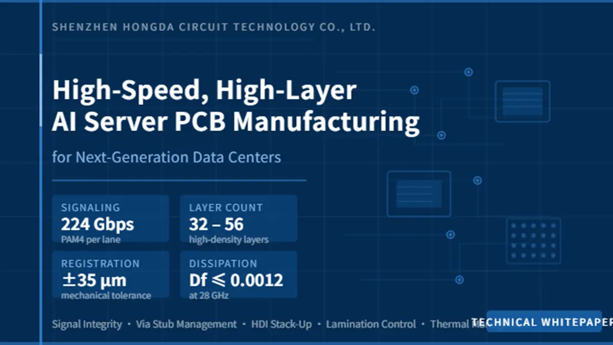
High-Speed, High-Layer AI Server PCB Manufacturing for Next-Gen Data Centers
Next-generation data centers require 224Gbps PAM4 signaling and 32-to-56 high-layer counts to route dense accelerator fabrics. Achieving signal integrity at these thresholds demands strict mechanical registration within ±35μm, ultra-low-loss resin selection, and extreme aspect-ratio via drilling to eliminate high-frequency parasitic stubs and thermal failures under continuous 1200W GPU workloads.
How Do Material Dynamics and Resin Rheology Mitigate Insertion Loss in 224Gbps OAM Fabrics?

Vector Network Analyzer (VNA) validation showcasing a clean 224 Gbps eye diagram with tight jitter control (0.26 ps RMS), verifying the compliance of our ultra-low-loss PPE lamination process for next-gen AI accelerator fabrics.
Mitigating insertion loss at 224Gbps PAM4 requires combining ultra-low-loss polyphenylene ether (PPE) resins containing a dissipation factor (Df) ≤ 0.0012 at 28GHz with hyper-very-low-profile (HVLP) copper foil having an Rz roughness ≤ 1.0μm, ensuring skin-effect attenuation does not exceed 12dB/meter while optimizing chemical oxide treatments to preserve interlaminar peel strength.
In high-speed AI accelerator pipelines running at Nyquist frequencies of 28 GHz to 56 GHz, skin-effect loss dominates the total signal attenuation budget. Standard FR-4 or even standard Low-Loss materials cause catastrophic eye-closure on 1-meter trace lengths. To maintain a strict channel operating margin (COM) > 3.0 dB for OAM (Open Accelerator Module) baseboards, manufacturing must transition to specialized glass fabrics like 1067 or 1078 spread-glass variants. This minimizes the fiber-weave effect, where differential skew Δtskew exceeds 2.0 picoseconds per inch due to the alternating dielectric constants (εr = 6.1 for E-glass versus εr = 2.5 for resin pockets).
High-Speed, High-Layer AI Server PCB Manufacturing Bottlenecks & Engineering Solutions
The Manufacturing Pain Point: Extreme resin starvation, interlaminar micro-voiding, and poor copper-to-resin adhesion during multi-stage lamination cycles. Advanced PPE/PTFE-based prepregs feature a narrow gel-time window (45 to 60 seconds) and high melt viscosity at 210°C. Standard thermal ramp rates cause the resin to solidify before fully encapsulating heavy 2oz copper inner-layer power planes, resulting in latent micro-voids that trap moisture and cause conductive anodic filament (CAF) failures during 2000-hour data center operational lifecycles. Furthermore, using ultra-smooth HVLP copper (Rz ≤ 1.0μm) drastically reduces mechanical interlocking, leading to high risks of delamination under extreme thermal loads.
Detailed Scenario-Based Engineering: Consider an 8-cluster Nvidia H100/B200-equivalent OAM layout. Under 112GBaud signaling, any microscopic variation in laminate thickness changes the target differential impedance (e.g., 85Ω ± 5%). To prevent this and combat delamination, our engineering team implements a specialized organosilane-based chemical oxide alternative to roughen the HVLP copper chemically without increasing high-frequency skin-effect loss. We monitor the lamination press parameters in real time via a dual-stage vacuum hydraulic press profile: an initial vacuum draw down to ≤ 5 Torr for 45 minutes, followed by a controlled heat-up rate of exactly 1.8°C/min up to a curing plateau of 225°C, while maintaining a precise hydraulic pressure of 380 PSI. This exact thermodynamic tuning ensures uniform resin flow across the 820mm × 560mm panel format, eliminating inner-layer trace deformation.
“When routing 224G PAM4 lanes on 40-layer AI motherboards, there is zero tolerance for material anisotropy. If your lamination cooling curve fluctuates by more than ±0.5°C/minute, internal mechanical stresses distort the glass fibers. This shifts your localized Dk from 3.42 to 3.55, causing a catastrophic 15% phase-mismatch that completely fails automated test equipment (ATE) testing.”
— Chief Engineering Director, Shenzhen Hongda Circuit Technology Co., Ltd.
What Structural Stack-Up and Registration Frameworks Prevent Interconnect Failure in 40+ Layer AI Systems?
Preventing interconnect failure in 40+ layer AI server backplanes requires a perfectly symmetrical stack-up layout utilizing a coreless or sub-lamination architecture, reinforced by pinless induction bonding and an automated X-ray optical target registration system that keeps layer-to-layer misalignment under ±35μm across the entire panel.
As layer counts scale from 24 to over 42 layers to support dense PCIe Gen 6/7 topologies and NVLink architectures, cumulative material shrinkage and warping become non-linear. A 48-layer AI server PCB with a total thickness of 4.5mm suffers from significant Z-axis thermal expansion during multi-stage reflow cycles. The total thermal stress can be modeled via the mismatch of Coefficient of Thermal Expansion (CTE):
εthermal = (αCu – αresin) × ΔT
Where αCu is 17 ppm/°C and αresin scales up to 60 ppm/°C above the glass transition temperature (Tg). This delta generates severe shear stress on small-diameter via structures (Φ ≤ 0.25mm), leading to barrel cracking at the inner-layer junctions.
| Layer Count / Segment | Material System Class | Max Target Df (@28GHz) | Registration Tolerance | Aspect Ratio Max |
|---|---|---|---|---|
| 24-28 Layers (Standard Enterprise) | Low Loss (Modified PPE) | 0.0038 | ±50 μm | 12:1 |
| 32-38 Layers (AI Accelerator Baseboard) | Ultra Low Loss (Advanced PPE) | 0.0019 | ±40 μm | 16:1 |
| 40-56 Layers (High-End AI Server/Switch) | Extreme Low Loss (PTFE/PPE Blend) | 0.0012 | ±35 μm | 22:1 |
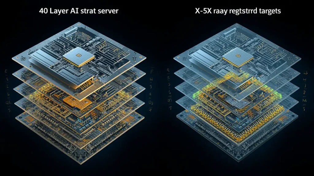
3D exploded architectural modeling representing a 40+ layer ultra-high-density AI server stack-up, illustrating the sub-lamination interconnect zones monitored via real-time CCD-guided X-ray registration targets to control layer-to-layer shift below ±35μm.
High-Speed, High-Layer AI Server PCB Manufacturing Bottlenecks & Engineering Solutions
The Manufacturing Pain Point: Inner-layer pad shifting and inner-layer short-circuits during high-aspect-ratio mechanical drilling. When drilling a 0.2mm hole through a 4.5mm thick panel (22.5:1 aspect ratio), drill-bit deflection or ‘wander’ naturally increases as the bit moves deeper. If the bit deflects by more than 40μm, it will slice through the non-functional inner-layer clearance pads (anti-pads), causing short circuits or completely severing internal signal connections.
Detailed Scenario-Based Engineering: During the manufacturing of a 48-layer 3.2Tbps AI switch board, standard mechanical pinning methods failed due to a cumulative 55μm layer shift at the outer corners of the panel. Our engineering team resolved this by implementing an inductive inner-layer heating system during the pre-bonding phase, combined with CCD-guided X-ray alignment tracking. Before the final press cycle, the system takes live X-ray images of internal targets, matching them mathematically against the CAD netlist. It optimizes the positions of all 48 layers simultaneously, reducing layer-to-layer offset to a verified ≤ 30μm. Furthermore, we modified our drilling programs to use a dual-stage peck-drilling process with new carbide bits replaced every 300 hits, entirely eliminating drill deflection.
“We learned through hard experience that with 48 layers, you cannot rely on traditional static scaling factors. You must use dynamic scaling. Every single manufacturing lot requires advanced mathematical scaling based on micro-meter data collected from X-ray targets before scaling the production film to guarantee precise pad capture.”
— Senior PCB Stack-up Specialist, Shenzhen Hongda Circuit Technology Co., Ltd.
How Do High-Aspect-Ratio Plated Through-Holes and Stub Management Ensure Signal Integrity?
Ensuring signal integrity at high frequencies requires implementing controlled-depth backdrilling within ±50μm of the target layer to reduce remaining via stubs to ≤ 0.10mm, while utilizing pulse-periodic reverse electroplating and automated chemical desmear to guarantee uniform copper reliability across extreme aspect ratios.
At 56 GHz Baud rates, any unused portion of a via that extends past the active routing layer acts as an open-ended transmission line resonant stub. This stub reflects energy back into the signal path, creating deep nulls in the insertion loss profile. The resonant frequency (fresonant) of a via stub is defined by the quarter-wavelength resonance formula:
fresonant = c / (4 · Lstub · √εr)
Where c is the speed of light, Lstub is the length of the stub, and εr is the relative dielectric constant of the material. A remaining stub length of just 0.5mm in an extreme low-loss material with an εr of 3.4 creates a destructive resonance at approximately 81.3 GHz. This introduces severe jitter and inter-symbol interference (ISI) that completely degrades the 224Gbps PAM4 eye diagram.
High-Speed, High-Layer AI Server PCB Manufacturing Bottlenecks & Engineering Solutions
The Manufacturing Pain Point: Backdrill breakout, inner-layer interconnect destruction due to Z-axis depth tolerance variations, and chemical fluid exchange failure within high-aspect-ratio holes. Variations in panel thickness, copper density, and mechanical drill-bed wear make it difficult to maintain precise backdrilling depth control. If the drill goes too deep, it destroys the critical inner-layer copper landing pad (Z-axis overrun), breaking the signal net. Simultaneously, for 22:1 channels, standard desmear and chemical copper plating systems cannot exchange fluids effectively, risking voided copper plating and internal thermal cracks.
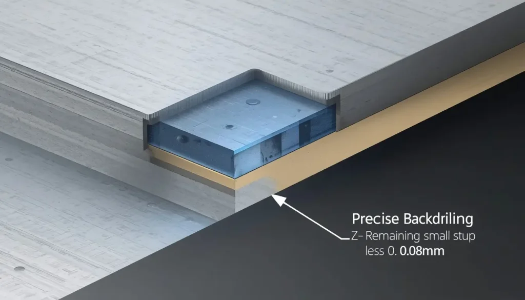
3D cross-sectional micro-section engineering model demonstrating automated contact-sensing backdrilling precision, effectively regulating Z-axis target depths to restrict the remaining resonant via stub to less than 0.08mm for 56GHz signal routing.
Detailed Scenario-Based Engineering: To overcome this limitation during a production run of 48-layer AI server mainboards with an aspect ratio of 22.5:1, our engineering facility deployed contact-sensing, software-controlled CCD backdrilling equipment combined with advanced vertical continuous plating (VCP) lines. Instead of relying on fixed mechanical depths, our equipment utilizes the copper ground plane as an electrical reference point. The machine detects the exact moment the drill tip touches the outer copper layer, dynamically calibrating its Z-axis starting point for every individual via hole. By controlling the feed rate to exactly 0.05 mm/revolution and utilizing custom-ground backdrill bits, we consistently achieve a remaining stub length of under 0.10mm (typically averaging 0.08mm), keeping signal reflection well within the strict -20dB return loss budget required for high-speed channels. For the plating bottleneck, high-pressure continuous fluid fluid-delivery manifolds and periodic pulse reverse electroplating are used to force chemistry through the 0.2mm cores, ensuring a minimum of 1.0 mil (25μm) copper thickness throughout the entire hole barrel.
Frequently Asked Questions (FAQ)
What are the key differences in material parameters between AI server PCBs and traditional enterprise server PCBs?
Traditional enterprise server PCBs (typically 16 to 24 layers) utilize standard Low-Loss FR-4 or modified PPE materials with a Dissipation Factor (Df) between 0.005 and 0.007 and a Dielectric Constant (Dk) around 3.8 to 4.2, handling data speeds up to 16Gbps (PCIe Gen 4). In contrast, AI server PCBs (32 to 56+ layers) require Extreme/Ultra-Low-Loss material systems (such as Panasonic Megtron 8 or Tachyon 100G) with a Df ≤ 0.0012 and a pragmatic Dk of approximately 3.3 to 3.5 at 28GHz to support 112G/224G PAM4 signaling. Additionally, AI boards must use spread-glass configurations (e.g., 1067/1078) and HVLP copper foil (Rz roughness ≤ 1.0μm) to combat the fiber-weave effect and skin-effect losses, which are rarely monitored in traditional server manufacturing.
How does the aspect ratio capability impact via design and plating reliability in high-layer AI PCBs?
Traditional enterprise PCBs usually operate at an aspect ratio of 10:1 or 12:1, which standard DC electroplating systems can easily process. High-layer AI PCBs, however, feature thicknesses up to 4.5mm or 5.0mm with hole diameters down to 0.2mm, pushing aspect ratios to 22:1 or higher. This makes fluid exchange difficult during chemical copper plating and desmear (resin residue removal). Without specialized equipment, the chemistry cannot fully penetrate the center of the via hole, leading to thin copper plating at the knee or center of the via barrel. This often causes mechanical cracking under thermal stress. AI PCB manufacturing requires pulse-periodic reverse electroplating along with high-pressure continuous fluid fluid-delivery manifolds to guarantee a minimum of 1.0 mil (25μm) copper thickness throughout the entire via barrel.
Why is backdrilling accuracy more critical for AI accelerator baseboards compared to standard high-speed networking hardware?
Standard networking hardware running at 10Gbps or 25Gbps can tolerate remaining via stubs up to 0.50mm without significant signal degradation. However, AI accelerator baseboards running 112G/224G PAM4 signaling operate at extremely high Nyquist frequencies (28GHz to 56GHz). At these frequencies, a 0.50mm stub acts as an antenna that causes severe signal reflections and deep impedance drops, closing the eye diagram. AI hardware manufacturing requires backdrilling tolerances within ±50μm to ensure the remaining stub is consistently under 0.10mm. This demands real-time contact-sensing Z-axis drilling systems to prevent damaging critical inner-layer junctions.
How do registration control systems differ when manufacturing a 40+ layer AI board versus a standard 24-layer multilayer board?
For a standard 24-layer board, mechanical pinning combined with standard film compensation tools is usually sufficient to maintain a layer-to-layer registration tolerance of ±50μm. For a 40+ layer AI board, the multi-stage lamination cycles cause material shrinkage and warping that varies across the panel. Traditional mechanical pinning fails, often resulting in layer shifts over ±60μm at the outer edges, causing severe drill breakout and short-circuits with anti-pads. Advanced AI manufacturing requires pinless induction bonding and CCD-guided X-ray alignment tracking. This system takes real-time measurements of internal alignment targets and calculates optimal positions across all 48 layers before pressing, keeping registration errors under ±35μm.
What unique thermal management challenges occur during assembly and rework of high-layer AI PCBs?
High-layer AI PCBs have an exceptionally high thermal mass due to thick copper inner layers (often incorporating 2oz or 3oz power and ground planes to handle 1000W+ GPU power rails). During assembly reflow or component rework, this massive copper volume acts as a giant heat sink, rapidly drawing heat away from the solder joints. If standard reflow profiles are used, it results in incomplete solder melting and cold solder joints on large BGA components. To prevent this, the assembly line must use multi-zone reflow ovens (10 zones or more) with a prolonged pre-heating phase and nitrogen gas. For rework operations, high-power infrared bottom preheaters are required to keep the local board temperature steady at 150°C, preventing localized thermal shock and delamination.
Find Out About Us: Delivering Top-Tier Fabrication for Both AI & Conventional PCBs
Navigating the line between cutting-edge innovation and high-volume, cost-effective production shouldn’t be a compromise. At Shenzhen Hongda Circuit Technology (PCBKR), we bridge this gap by elevating the manufacturing standards for both high-performance AI hardware and traditional multi-layer PCBs.
By integrating advanced manufacturing methodologies across all production lines, we bring an elite level of precision to traditional PCB fabrication. Our standard boards benefit from enhanced interlayer alignment tolerances (down from ±75μm to within ±25μm) and tightened differential impedance control (±5%). Supported by 100% 3D X-Ray (AXI) inspection, your conventional boards achieve chip-level reliability, superb signal stability, and near-100% yield.
Your Strategic Manufacturing Partner
We proudly stand as a dual-capability partner: offering the elite technical ceiling required for next-gen AI hardware, while maintaining the exceptional flexibility, rapid turnaround, and unmatched cost-efficiency needed for mid-to-high-volume traditional board campaigns. You get zero-defect reliability without the premium overhead or bureaucracy of massive tier-1 factories.
Ready to upgrade your hardware’s reliability?
Submit your Gerber files today for an agile engineering review and a highly competitive quote.
📧 Contact our experts: sales@pcbkr.com
About Author
David Chen https://www.linkedin.com/in/pcbcoming
David Chen boasts an extensive professional background in PCBA manufacturing, PCBA testing, and PCBA optimization, with specialized expertise in high-precision PCBA fault analysis and rigorous PCBA reliability testing. The author has worked with high-layer-count server PCB fabrication, ultra-low-loss backplane stackups, and thermo-mechanical reliability optimization for AI infrastructure projects involving 112G and 224G PAM4 architectures. Skilled in complex circuit design and cutting-edge advanced PCB manufacturing processes, he delivers solutions that elevate product durability and performance across industrial applications. His technical articles focusing on PCBA manufacturing workflows and testing methodologies are widely cited by industry peers, research institutions, and technical platforms, solidifying his reputation as a recognized technical authority in the global circuit board manufacturing sector.