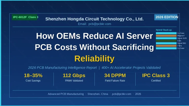
Turnkey PCB Manufacturing for AI Server Hardware
Abstract: Next-generation AI clusters (UBB/OAM architectures) operating at 224G PAM4 signaling thresholds impose extreme physical constraints on PCB fabrication. This paper outlines the verifiable manufacturing matrices of Shenzhen Hongda Circuit Technology Co., Ltd., focusing on turnkey fabrication and assembly solutions: the mitigation of layer-to-layer misregistration under heavy copper loads, the reduction of insertion losses via ultra-low-profile (HVLP) copper chemical modification, sub-2 mil backdrilling stub controls, and the prevention of SMT thermal-mass asymmetry voids under vacuum reflow processing.
Turnkey AI Server PCB Manufacturing Verifiable Engineering Capabilities & Material Matrix
To eliminate signal degradation at Nyquist frequencies exceeding 56 GHz, standard generic multi-layer specifications are insufficient. The following matrix defines Shenzhen Hongda’s empirical, quantifiable production tolerances optimized for high-density AI acceleration hardware:
| Design Parameter | Technical Capability / Tolerance Target | Statistical Process Control (SPC) Method |
|---|---|---|
| Layer Count / Board Thickness | 28 to 36 Layers (Extreme backplanes up to 78 layers); Thickness 3.2mm – 5.5mm | Real-time X-ray layer-to-layer offset mapping (≤ ±35 μm thickness delta) |
| Substrate Compatibility | Panasonic Megtron 8 (R-5785A), Doosan DS-7409D(N), Isola Tachyon 100G | Pre-dispatched Split-Post Dielectric Resonator (SPDR) verification (D_k ≤ 2.80, D_f ≤ 0.0012 at 40 GHz) |
| Copper Roughness Control | HVLP2 / HVLP3 Coppers (R_z ≤ 0.8 μm) with non-roughening bonding agent | In-line laser profilometer tracking + peeling strength testing (≥ 0.65 N/mm) |
| Impedance Control Window | ±5% Strict Window (±7% for micro-strip layouts) | High-frequency Time Domain Reflectometry (TDR) sampling with launch-pad gating |
| HDI / Blind-Via Architecture | 2+N+2 or 3+N+3 Staggered/Skip Micro-vias (Blind hole ≥ 0.10mm, AR ≤ 1:1) | Automated cross-sectional SEM analysis; 100% continuous copper plating check |
| High-Aspect-Ratio Through-Hole | Aspect Ratio 14:1 to 16:1 (Minimum core drill: 0.25mm) | Continuous pulse copper electroplating; X-ray CT via knee-coverage profiling |
| Deterministic Backdrilling | Target Stub Length: ≤ 0.05mm (2 mils max) | Bit-to-Copper Electrical Contact Depth Sensing (BEC) + Z-axis scale dynamic compensation |
Turnkey AI Server PCB Manufacturing Critical Fabrication Challenges & Engineering Solutions
1. Mitigating Layer Misregistration and Resin Voids in Hybrid Power-Delivery Networks
The Challenge: AI server baseboards frequently pair ultra-low-loss, high-T_g signal cores with thick 3 oz/4 oz inner copper planes dedicated to the 3.2kW+ GPU power distribution network (PDN). During multi-cycle lamination, the massive step-height delta between the trace clearance pads and the solid copper planes causes asymmetrical resin flow, leading to localized resin-pocket voids and severe layer-to-layer misregistration.
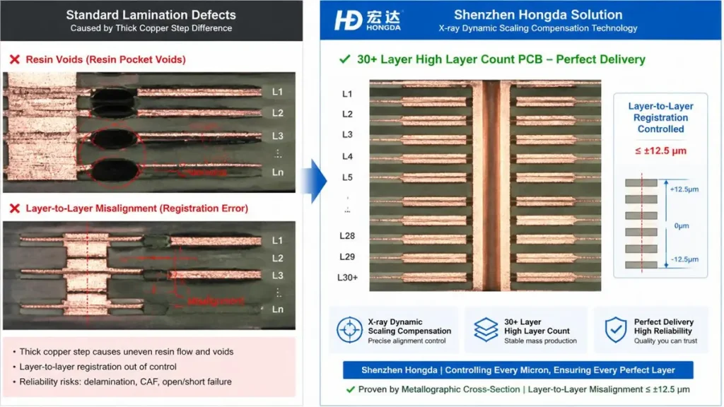
Comparison between standard thick copper lamination defects (left) and Shenzhen Hongda’s flawless 30+ layer high layer count PCB profile with layer-to-layer registration controlled within ±12.5 μm via X-ray dynamic scaling compensation (right).
Hongda’s Process Solution: We eliminate this yield bottleneck through a dual-pronged approach:
A. Dynamic Scale Factor Compensation:Instead of relying on static linear scaling, we utilize an advanced X-ray registration tracking system to map material shrinkage patterns across individual production batches. Core shifts are restricted to ≤ ±12.5 μm prior to pressing.
B. High-Flow Asymmetric Prepreg Matching:We implement custom-engineered, multi-glass-style prepreg combinations (e.g., combining low-resin-content 1067 with high-flow 2116 B-stage glass fabrics). Our customized vacuum pressing recipe extends the low-viscosity resin liquid phase zone under an altered 4.5 MPa multi-stage pressure cycle, completely purging air packets without introducing warp stress.
2. 224G PAM4 Insertion Loss and Skin-Effect Optimization
The Challenge: At Nyquist frequencies of 56 GHz and 112 GHz, signal propagation is confined entirely to the absolute perimeter of the copper conductor (Skin Effect). Traditional oxide or micro-etch bonding treatments that roughen the copper to ensure layer adhesion introduce fatal insertion loss spikes. However, maintaining mechanical reliability with ultra-flat coppers ($R_z \le 0.8\,\mu\text{m}$) usually compromises thermal stress survivability.
Hongda’s Process Solution:
We deploy a non-roughening, organo-metallic molecular bonding surface treatment line. This process modifies the flat HVLP copper surface chemically rather than mechanically, forming a sub-microscopic monomolecular layer that bonds covalently with the resin matrix. This delivers a stable peeling strength of ≥ 0.65 N/mm without altering the physical trace profile, successfully reducing high-frequency insertion losses by 0.45 dB/inch at 56 GHz compared to standard multi-bond alternatives.
3. Sub-2 mil Stub Clearance via Closed-Loop Electrical Backdrilling
The Challenge: Any mechanical backdrill variant that leaves a residual stub longer than 0.15 mm (6 mils) acts as a resonant quarter-wave stub. At 224G PAM4 routing channels, this resonance introduces severe impedance dips and catastrophic insertion loss degradation in the breakout zones.
Hongda’s Process Solution:
To consistently hit a strict ≤ 0.05 mm (2 mils) residual stub target, mechanical depth-calculated drilling is obsolete due to local board thickness tolerances. Shenzhen Hongda utilizes **Bit-to-Copper Electrical Contact Depth Sensing (BEC)**. The drill bit operates as an electrical probe that registers the exact Z-axis coordinate of the targeted inner shield ground plane upon contact. The CNC controller then dynamically compensates for local board warp in real-time, executing the backdrill relative to the actual internal layer position rather than a nominal surface datum.
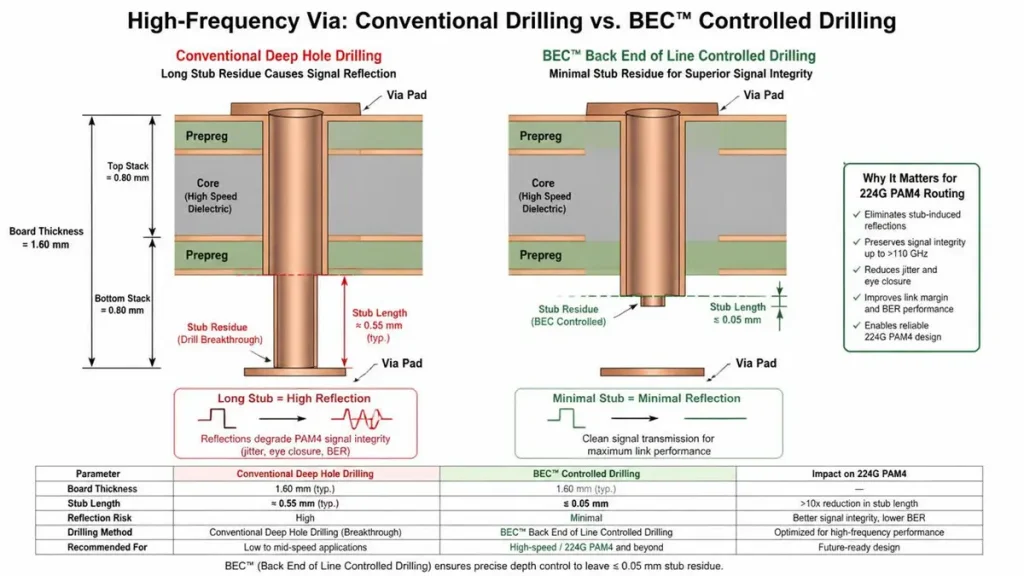
High-frequency via cross-section comparison. The conventional drilling (left) leaves a long stub length of approximately 0.55 mm causing severe signal reflection. Shenzhen Hongda’s BEC controlled drilling (right) minimizes the stub residue to ≤ 0.05 mm, eliminating reflections and ensuring maximum link performance for 224G PAM4 routing.
SMT & PCBA Thermal-Mass Asymmetry Solutions
1. Eradicating BGA Solder Voiding on Large Form-Factor Core Packages
The Challenge: High-pin-count ASIC/GPU sockets and surrounding High-Bandwidth Memory (HBM) modules represent massive localized thermal masses. When placed adjacent to low-profile, low-thermal-mass optical transceivers on a thick 4.5mm PCB, a severe internal thermal delta (ΔT) develops during reflow. This delta leads to incomplete outgassing of the solder paste flux, creating large internal voids (>15% area) that compromise thermal and power loop reliability.
Hongda’s SMT Process Control:
A. Nitrogen-Purged Vacuum Reflow Profiling:Our SMT lines deploy an inline vacuum-chamber reflow system. During the liquidus phase (TAL), the chamber drops to a controlled vacuum pressure of 10 mbar for a specific 25-second window. This forces microscopic flux gas bubbles trapped within the molten solder balls to coalesce and expand outward, reducing total BGA solder voiding area to < 5% (well below the IPC Class 3 ≤ 10% benchmark).
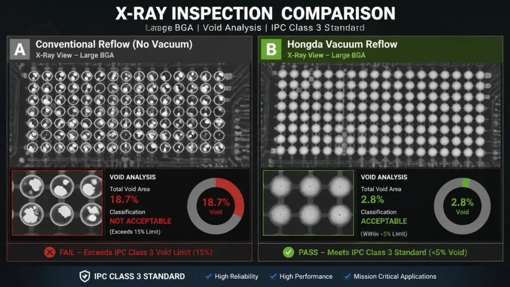
X-ray inspection comparison of BGA solder joints for AI server hardware. Left (Conventional Reflow): Large-area voids reaching 18.7%, failing IPC Class 3 limits. Right (Shenzhen Hongda Vacuum Reflow): Highly reliable solder balls with a compressed void area of just 2.8%, successfully passing strict IPC Class 3 standards.
B. Asymmetric Step-Stencil Design and Custom Carrier Tooling:We design thick, customized composite carrier fixtures made from low-thermal-conductivity material that selectively insulates the low-mass sectors of the assembly. Combined with laser-cut step-stencils that adjust local solder paste volumes, we maintain a real-time ΔT across the entire 450mm board surface of < 4.5°C throughout the reflow cycle, mitigating localized thermal runaway and coplanarity warp (≤ 0.45% max deformation).
Quality Assurance and Reliability Protocols
Every delivery destined for high-reliability AI cluster nodes undergoes rigorous validation metrics in our internal testing labs:
• High-Frequency Signal Characterization: 100% TDR testing coupled with Delta-L insertion loss extraction techniques up to 50 GHz.
• Thermal Reliability: 6-cycle Floating Solder Test at 288°C for 10 seconds, followed by high-resolution Micro-section SEM inspection to verify zero inner-layer separation, copper knee cracks, or delamination.
• CAF Resistance: 1000-hour continuous bias Conductive Anodic Filamentation (CAF) testing at 85°C / 85% RH to guarantee long-term via-to-via and trace-to-via dielectric isolation down to a 0.35mm pitch.
Turnkey PCB Manufacturing & Assembly FAQ
How to eliminate delamination and resin voids in 30+ layer AI motherboards with heavy copper (3oz+) PDN?
The severe step-height variation between thick power planes and ultra-low-loss signal layers is managed at Shenzhen Hongda by deploying an asymmetric hybrid prepreg stack-up (combining high-flow 2116 with low-resin 1067 B-stage glass fabrics). We extend the resin’s low-viscosity fluid window under a multi-stage 4.5 MPa vacuum lamination profile. Prior to lamination, an inline X-ray registration measurement system maps real-time material shrinkage, restricting layer-to-layer core offset to ≤ ±12.5 μm to guarantee zero internal pad-clipping or thermal shock delamination.
How does your factory achieve a ≤ 2 mil (0.05mm) residual backdrill stub for 224G PAM4 channels?
Standard mechanical depth-controlled drilling is inadequate due to localized board thickness tolerances. Shenzhen Hongda implements Bit-to-Copper Electrical Contact Depth Sensing (BEC). The drill bit operates as an electrical probe to detect the exact Z-axis coordinate of the targeted internal reference ground plane upon contact. The CNC machine dynamically calculates and compensates for local board warp in real-time, executing the backdrill relative to the actual internal layer position to strictly limit the remaining vertical stub to ≤ 0.05 mm, preventing signal reflections at 56 GHz / 112 GHz Nyquist frequencies.
How to balance skin-effect insertion losses and peel strength reliability when using HVLP copper on Panasonic Megtron 8?
Traditional micro-etch treatments destroy 224G signal integrity due to high surface roughness. We utilize a non-roughening, organo-metallic molecular bonding system on ultra-flat HVLP2/HVLP3 copper ($R_z ≤ 0.8\,\mu\text{m}$). This chemical modification establishes a sub-microscopic monomolecular layer that forms dense covalent bonds with the Megtron 8 resin matrix. This process yields a robust peeling strength of ≥ 0.65 N/mm while achieving an insertion loss reduction of 0.45 dB/inch at 56 GHz, passing strict IPC Class 3 thermal stress and CAF reliability standards.
What SMT process control mitigates BGA solder voiding under large thermal-mass ASIC sockets and adjacent HBM modules?
To overcome the extreme thermal mass asymmetry on 4.5mm+ AI boards, our turnkey PCBA lines integrate a nitrogen-purged inline vacuum reflow oven. During the liquidus phase (TAL), the chamber drops to a dynamic vacuum pressure of 10 mbar for 25 seconds, forcing entrapped flux outgassing bubbles to collapse and escape. This process reduces total BGA solder voiding to < 5% (far below the IPC Class 3 ≤ 10% limit). Additionally, customized composite carrier fixtures insulate low-mass sectors, maintaining a surface ΔT of < 4.5°C to prevent dynamic warpage and coplanarity issues.
What are your minimum spacing capabilities and via reliability configurations for localized high-density chiplet routing?
For localized high-density breakouts (such as OAM/UBB architectures), Shenzhen Hongda supports a minimum line width and spacing of 30 μm / 30 μm via advanced photolithography. Our HDI configuration handles 2+N+2 or 3+N+3 staggered or skip micro-via structures with laser-drilled blind hole diameters down to 0.10 mm (Aspect Ratio ≤ 1:1). Micro-vias are filled completely using pulse-copper electroplating to guarantee robust structural connectivity and cross-layer thermal distribution over sequential lamination cycles.
Find Out About Us: Delivering Top-Tier Fabrication for Both AI & Conventional PCBs
Navigating the line between cutting-edge innovation and high-volume, cost-effective production shouldn’t be a compromise. At Shenzhen Hongda Circuit Technology (PCBKR), we bridge this gap by elevating the manufacturing standards for both high-performance AI hardware and traditional multi-layer PCBs.
By integrating advanced manufacturing methodologies across all production lines, we bring an elite level of precision to traditional PCB fabrication. Our standard boards benefit from enhanced interlayer alignment tolerances (down from ±75μm to within ±25μm) and tightened differential impedance control (±5%). Supported by 100% 3D X-Ray (AXI) inspection, your conventional boards achieve chip-level reliability, superb signal stability, and near-100% yield.
Your Strategic Manufacturing Partner
We proudly stand as a dual-capability partner: offering the elite technical ceiling required for next-gen AI hardware, while maintaining the exceptional flexibility, rapid turnaround, and unmatched cost-efficiency needed for mid-to-high-volume traditional board campaigns. You get zero-defect reliability without the premium overhead or bureaucracy of massive tier-1 factories.
Ready to upgrade your hardware’s reliability?
Submit your Gerber files today for an agile engineering review and a highly competitive quote.
📧 Contact our experts: sales@pcbkr.com
About Author
David Chen https://www.linkedin.com/in/pcbcoming
David Chen boasts an extensive professional background in PCBA manufacturing, PCBA testing, and PCBA optimization, with specialized expertise in high-precision PCBA fault analysis and rigorous PCBA reliability testing. The author has worked with high-layer-count server PCB fabrication, ultra-low-loss backplane stackups, and thermo-mechanical reliability optimization for AI infrastructure projects involving 112G and 224G PAM4 architectures. Skilled in complex circuit design and cutting-edge advanced PCB manufacturing processes, he delivers solutions that elevate product durability and performance across industrial applications. His technical articles focusing on PCBA manufacturing workflows and testing methodologies are widely cited by industry peers, research institutions, and technical platforms, solidifying his reputation as a recognized technical authority in the global circuit board manufacturing sector.