Why Choose Custom AI Server PCB Production in China?
China dominates the custom AI server PCB manufacturing market by integrating an ultra-dense electronics ecosystem, advanced ultra-low-loss material supply chains, and high-layer rigid-flex engineering capabilities that compress standard production cycles by 40%.
Introduction: Why AI Servers Require Custom PCB Manufacturing
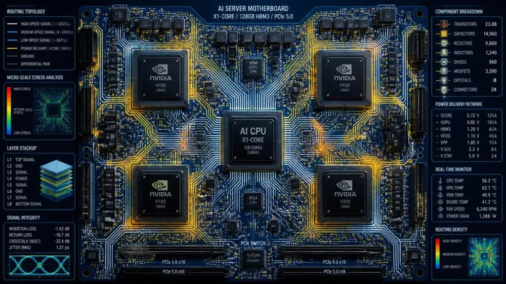
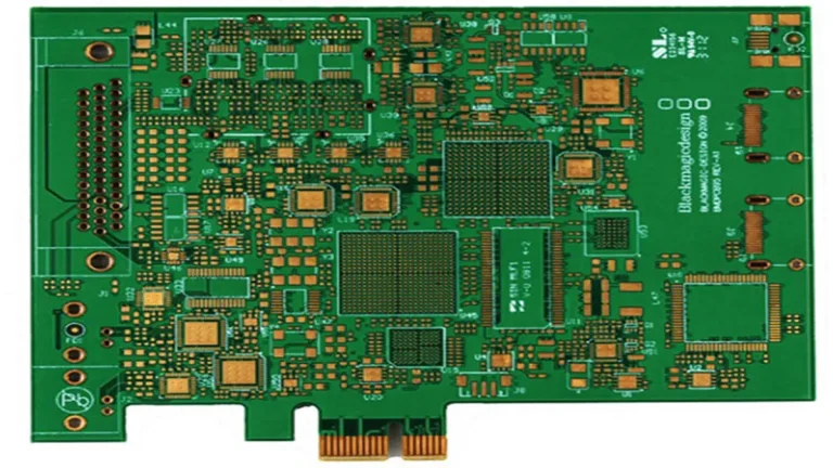
AI Server Motherboard Routing Topology & Stress Analysis – Shenzhen Hongda Circuit
Why Standard PCBs Cannot Meet the Requirements of AI Servers
Traditional standard PCBs use common FR-4 substrates with conventional layouts. Their dissipation factor is as high as Df ≈ 0.020, making it impossible to stay within the strict insertion loss budgets required for 112G or 224G PAM4 high-speed signal transmissions. Furthermore, standard PCBs face extreme thermal and power challenges from high-performance AI chips, creating severe risks of substrate carbonization, delamination, or via cracking.
- High-Speed and Ultra-High Bandwidth Demands: Along with the explosive growth of large AI models and supercomputing clusters, data transmission rates between AI accelerators (such as OAM modules) and UBB motherboards have leaped beyond 56G PAM4 into the 112Gbps and 224Gbps SerDes era. At these ultra-high frequencies, the skin effect becomes severe, causing massive signal distortion on standard PCB traces.
- Extreme Layer Counts and High-Density Form Factors: AI server motherboards must host complex CPUs, GPUs, HBM memory stacks, and extensive PCIe 6.0/7.0 channels. Consequently, board layer counts must reach 24 to over 60 layers. Standard materials exhibit an excessively large coefficient of thermal expansion along the Z-axis (Z-CTE) under high-temperature multi-layer lamination, which fails to guarantee registration accuracy across layers.
- Extreme Thermal Pain Points: Modern single AI chips can consume 700W or more. Massive heat accumulates at the base of dense BGAs. Because standard circuit boards cannot run reliably in environments where Tg ≤ 150°C, they demand deeply customized thermal designs utilizing special metal bases, buried copper blocks, or heavy copper power distribution networks (PDN).
AI Server PCB Production in China Supply Chain Advantages
How Does China’s PCB Supply Chain Empower Global AI Customers?
China has established the world’s only closed-loop B2B manufacturing ecosystem that spans from ultra-low-loss copper-clad laminates, specialty fiberglass cloths, and HVLP ultra-low-profile copper foils to high-precision forming and automated high-frequency testing, speeding up localized sourcing for critical components and accessories by over 3 times.
- Seamless Sourcing of Core Raw Materials: In the latest AI hardware stack designs, Panasonic Megtron 8 (R-5795U), Megtron 7 (R-5785), and Isola I-Tera are recognized as the premier material choices. As an industry expert, Shenzhen Hongda Circuit Technology Co., Ltd. has established direct supply networks with global top-tier laminate manufacturers. Even during supply tight cycles for specialty glass cloths, we maintain priority access to premium spread glass cloths, which are critical for controlling glass weave skew across differential pairs at 56G+ PAM4 speeds.
- Mature Industrial Cluster Effects: Relying on mature electronic manufacturing clusters centered around Shenzhen, Dongguan, and Suzhou, we can mobilize complete upstream and downstream resources within a one-hour drive. Every step—from Design for Manufacturability (DFM) reviews and HDI blind/buried via processing to downstream PCBA surface mounting and 100-Gbps-level high-speed blind testing—is seamlessly linked.
- One-Stop High-Efficiency Delivery Transformation:
| Stage | Traditional Fragmented Supply Chain | Shenzhen Hongda Circuit One-Stop Cycle |
| Large-Pitch BGA 32-Layer Motherboard Prototype | 18 – 25 Days | 7 – 10 Days |
| High-Speed Material Sourcing & Stackup Development | 30 Days (Overseas allocation) | 3 – 5 Days (Local regular stock) |
| DFM Simulation & Signal Integrity Feedback | 5 Days | Within 24 Hours |
AI Server PCB Production in China Custom Capabilities: Engineering, Cost, and Lead Time
What Specific Indicators Can Hongda Circuit Provide for Custom AI Server PCBs?
Hongda Circuit offers extreme engineering customization capabilities, supporting layer counts above 60 layers, 112G/224G high-speed impedance control, minimum trace width/spacing ≤ 1.5 mil, and deep back-drilling technology, eliminating errors between prototyping and mass production while keeping multi-layer board pricing highly competitive.
Expert-Level Original Engineering Experience and Technical Insights
- Advanced DFM and SI/PI Optimization:
“At 112G PAM4 high frequencies, any tiny via stub acts as a lethal RF resonator. When reviewing AI motherboard designs, we not only require strict impedance tolerances within ±5%, but we also mandate that the signal via stub depth must be kept ≤ 8 mil (with a target of < 5 mil). Additionally, Power Integrity (PI) designs must run frequency-domain simulations for AC/DC impedance. Because the operating current is exceptionally high, our resin content calculations for multi-layer boards with heavy copper over 2oz are precise to 0.01 mm to prevent micro-voids caused by insufficient resin flow during lamination, which can lead to high-voltage Conductive Anodic Filament (CAF) failures.” — From the practical log of Hongda Circuit’s Chief Engineer
- Parameterizable and Verifiable Manufacturing Metrics:
- Ultra-High Layer Stacking Technology: Stable mass production from 16 to 40+ layers, with an extreme capability reaching 60 layers for rigid motherboard lamination.
- Material Matrix: Standard options include Megtron 8 (Df = 0.0012 @ 14 GHz), Megtron 6, and Tachyon 100G, completely paired with HVLP (Hyper Very Low Profile) copper foil with a surface roughness of Rz < 1 µm to minimize skin effect losses.
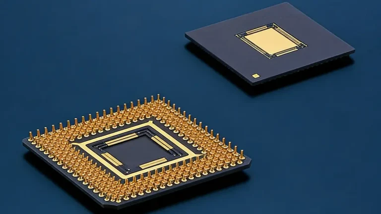
- Mechanical & Laser Microvias: Supports multi-stage HDI structures (e.g., 1+N+1, 2+N+2, Anylayer), with a minimum laser via diameter of 0.075 mm.
Back-drilling: Proprietary depth-controlled flash drilling technology that keeps depth tolerances precisely within ±0.05 mm.
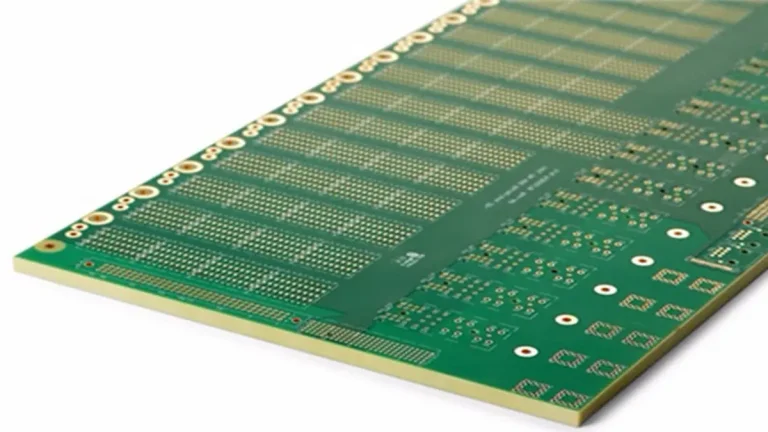
High-Layer High-Speed PCB Manufacturing Capabilities
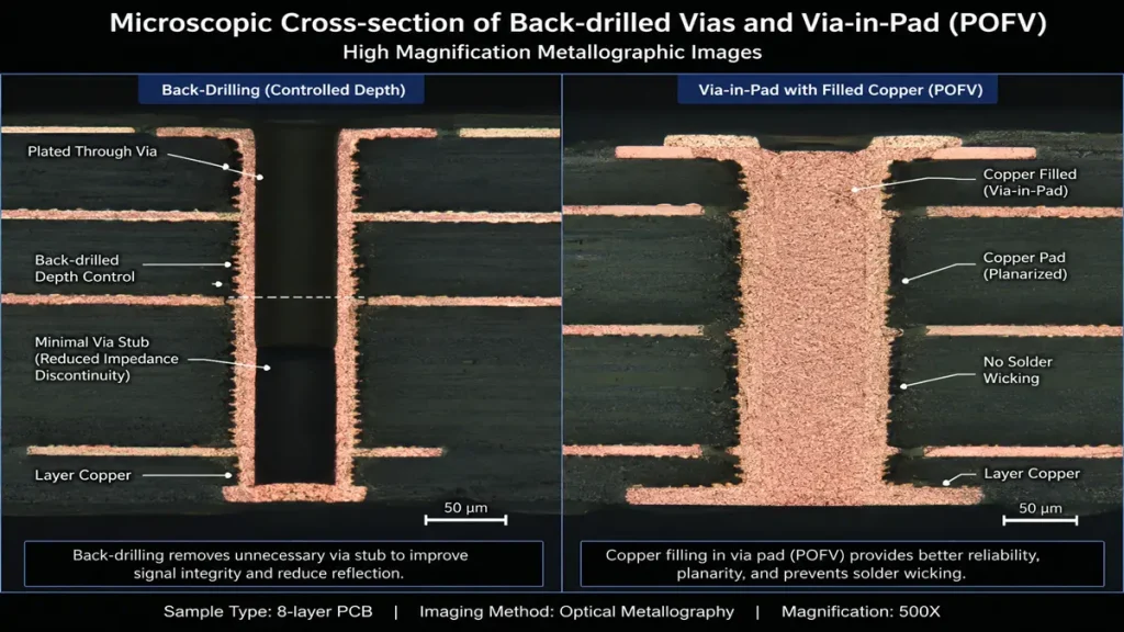
Microscopic Cross-section of Back-drilled Vias and Via-in-Pad (POFV) – Hongda Circuit
Facing AI GPU Server Motherboards, How Do Hongda Circuit’s Core Processes Solve the Industry Pain Point of Signal Loss?
To address the pain point of ultra-dense routing on AI GPU motherboards, we completely eliminate stray capacitance at pin pads by introducing the latest upgraded Plating Over Filled Via (POFV / Via-in-Pad) process and a high-precision impedance compensation system, ensuring high-fidelity transmission for 100G+ signals.
Detailed Manufacturing Scenario and Pain Point Analysis
When manufacturing an AI GPU server motherboard similar to the NVIDIA HGX/DGX architecture, thousands of BGA pins with pitches of 0.8 mm or smaller are packed onto the board surface to accommodate high-bandwidth NVLink cross-connections.
- Scenario Pain Point: Traditional trace fan-outs cause impedance discontinuities. If conventional Via-in-Pad structures are used without completely flat plating, trapped air bubbles can cause solder voids or solder paste migration during surface mount assembly, resulting in severe open circuits or impedance spikes.
- Hongda Circuit’s Solution: We use fully automated vacuum plugging machines to fill the vias with high-thermal-conductivity resin, followed by nano-level ceramic brush polishing after curing, and finally cap plating. This keeps the pad surface warp ≤ 5 µm. It provides an excellent thermal pathway while achieving zero reflection at the pad.
- Reliable Thermal Management Technology: To handle high thermal loads, we integrate heavy-duty thermal copper blocks within the inner layers. Even after 6 lead-free reflow cycles at up to 260°C, the overall multi-layer alignment remains locked within ≤ 1.5 mil, perfectly avoiding delamination or blistering caused by thermal stress.
Quality, Communication, and Compliance Issues
How to Resolve Information Asymmetry and Quality Concerns for International Customers Sourcing AI Server PCBs Overseas?
Hongda Circuit uses 100% Automated Optical Inspection (AOI) and 3D X-Ray inner layer registration validation, paired with real-time technical support handled directly by senior English-fluent Electronics Engineers (EEs), fully complying with RoHS, REACH, and the highest standards of intellectual property protection.
- Comprehensive Inspection Loop: High-layer AI server PCBs cannot rely on manual visual checks. Hongda Circuit mandates that all high-layer boards must pass the following before leaving the factory:
- Inner/Outer Layer Automated AOI: Eliminates tiny copper slivers and line-edge burrs.
- 3D X-Ray Registration Check: Verifies inner-layer alignment and target drilling accuracy after high-layer lamination.
- 100% Continuity and Short Testing: Performed using flying probe testers and dedicated ICT fixtures.
- Time Domain Reflectometry (TDR) Testing: Generates trace-by-trace impedance curve reports for all high-speed channels.
- Seamless International Communication: Our technical sales team consists of professional engineers with over 5 years of hands-on PCB factory production or RF simulation experience. They can perform live DFM reviews with your design teams directly using Altium Designer, Allegro, or ODB++ formats, entirely eliminating time-zone misunderstandings.
- Compliance and Strict IP Protection: We deploy a rigorous data leakage prevention system internally. We sign internationally enforceable NDAs for customer AI hardware schematics and Gerber files, and processing data runs on physically isolated local area networks to fully protect your core hardware intellectual property.
How to Choose the Right Chinese PCB Manufacturing Partner
What Quantitative Indicators and Red Flags Must Be Checked When Evaluating an AI High-Speed PCB Supplier?
You must thoroughly verify whether they have a proven mass production track record for 56G/112G PAM4 projects, routine processing experience with high-precision materials, and immediately disqualify low-end shops that lack complete high-speed testing equipment and DFM technical support.
- Key Evaluation Checklist:
- Engineering Depth: Does the supplier proactively identify impedance deviations in your stackup due to uneven dielectric thickness, rather than blindly processing “as-is”?
- Supply Chain Leverage: Does the supplier hold stable purchasing quotas and process certifications for high-end materials like the Panasonic Megtron series or Isola series?
- Critical Red Flags to Watch For:
- Vague Impedance Control: Inability to provide live TDR simulation reports, or claiming that impedance tolerances can only be held to ±10% (AI server boards require ±5% to ±7%).
- Process Deficiencies: Lacking precision back-drilling capabilities or showing unstable depth control, resulting in stubs exceeding 15 mil.
- Practical Advice: For complex AI GPU or NPU accelerator boards, always insist on a 1-5 panel small batch prototype run (MP Run / Prototype Validation) before moving to thousand-piece mass production, and use a Vector Network Analyzer (VNA) to verify actual insertion loss curves.
Frequently Asked Questions (FAQ)
What low-loss laminate combinations can you provide for the latest 112G/224G PAM4 AI chip motherboards?
We routinely process the latest Panasonic Megtron 8 (R-5795U) and Megtron 7 (R-5785) materials. Megtron 8 offers an industry-leading ultra-low dissipation factor of Df = 0.0012. To optimize project costs, we also excel at designing hybrid stackups: running Megtron 8/7 on critical high-speed signal layers while using high-Tg standard FR-4 materials for ordinary power and low-speed control layers. This maintains ultimate signal integrity while cutting overall bare board material costs by 30% – 40%.
How does Hongda Circuit guarantee accuracy during deep back-drilling on high-layer AI server PCBs?
The total thickness of high-layer boards (such as 32-layer boards) often exceeds 3.2 mm, making mechanical back-drilling risky if it penetrates internal trace layers. We utilize automated depth-controlled flash drilling guided by CCD cameras, which aligns via sensing targets built into the panels to keep Z-axis depth control within ±0.05 mm. This allows us to stably compress the remaining via stub to around 5 mil, completely blocking secondary signal wave reflections at 28GHz / 56GHz Nyquist frequencies.
Why do you strongly recommend Plating Over Filled Via (POFV) technology for dense BGA areas on AI servers?
Because AI motherboards handle massive bus bandwidth, BGA pin pitches are often compressed to 0.8 mm or lower. Traditional trace fan-outs take up valuable routing real estate and introduce parasitic inductance. By using Plating Over Filled Via (POFV) technology, vias are placed directly inside the component pads, filled with non-conductive resin, and planarized with copper cap plating. This guarantees flat pads, avoiding tombstoning or cold joints during SMT assembly while shortening the transmission path.
How does Hongda Circuit maintain delivery and price advantages amid supply chain fluctuations for CCL and specialty glass cloths?
Raw materials like low-loss copper-clad laminates and prepregs experience supply chain volatility. Because we maintain long-term strategic procurement agreements with leading domestic and international laminate suppliers like Panasonic, Isola, and Shengyi, we enjoy priority material allocations, ensuring our core high-speed inventory avoids stockouts. Paired with automated production lines and a high first-pass yield rate (≥ 98.5%), we dramatically lower internal scrap costs, passing those savings on to global B2B clients.
How does your engineering team assist Western clients with early-stage DFM challenges?
We break away from the traditional passive factory model of “just take the finished Gerber and print it.” Our engineering team consists of hardware and RF simulation experts. During your early architecture phase, you can share your stackup concepts with us, and we will calibrate trace widths and spacings to match target impedance models using professional signal integrity software within 24 hours. Before production begins, we proactively flag any risks regarding resin starvations during high-layer lamination or glass weave misalignments, ensuring a successful first-time build.
Find Out About Us: Delivering Top-Tier Fabrication for Both AI & Conventional PCBs
Navigating the line between cutting-edge innovation and high-volume, cost-effective production shouldn’t be a compromise. At Shenzhen Hongda Circuit Technology (PCBKR), we bridge this gap by elevating the manufacturing standards for both high-performance AI hardware and traditional multi-layer PCBs.
By integrating advanced manufacturing methodologies across all production lines, we bring an elite level of precision to traditional PCB fabrication. Our standard boards benefit from enhanced interlayer alignment tolerances (down from ±75μm to within ±25μm) and tightened differential impedance control (±5%). Supported by 100% 3D X-Ray (AXI) inspection, your conventional boards achieve chip-level reliability, superb signal stability, and near-100% yield.
Your Strategic Manufacturing Partner
We proudly stand as a dual-capability partner: offering the elite technical ceiling required for next-gen AI hardware, while maintaining the exceptional flexibility, rapid turnaround, and unmatched cost-efficiency needed for mid-to-high-volume traditional board campaigns. You get zero-defect reliability without the premium overhead or bureaucracy of massive tier-1 factories.
Ready to upgrade your hardware’s reliability?
Submit your Gerber files today for an agile engineering review and a highly competitive quote.
Contact our experts: sales@pcbkr.com
About Author
David Chen https://www.linkedin.com/in/pcbcoming
David Chen boasts an extensive professional background in PCBA manufacturing, PCBA testing, and PCBA optimization, with specialized expertise in high-precision PCBA fault analysis and rigorous PCBA reliability testing. The author has worked with high-layer-count server PCB fabrication, ultra-low-loss backplane stackups, and thermo-mechanical reliability optimization for AI infrastructure projects involving 112G and 224G PAM4 architectures. Skilled in complex circuit design and cutting-edge advanced PCB manufacturing processes, he delivers solutions that elevate product durability and performance across industrial applications. His technical articles focusing on PCBA manufacturing workflows and testing methodologies are widely cited by industry peers, research institutions, and technical platforms, solidifying his reputation as a recognized technical authority in the global circuit board manufacturing sector.