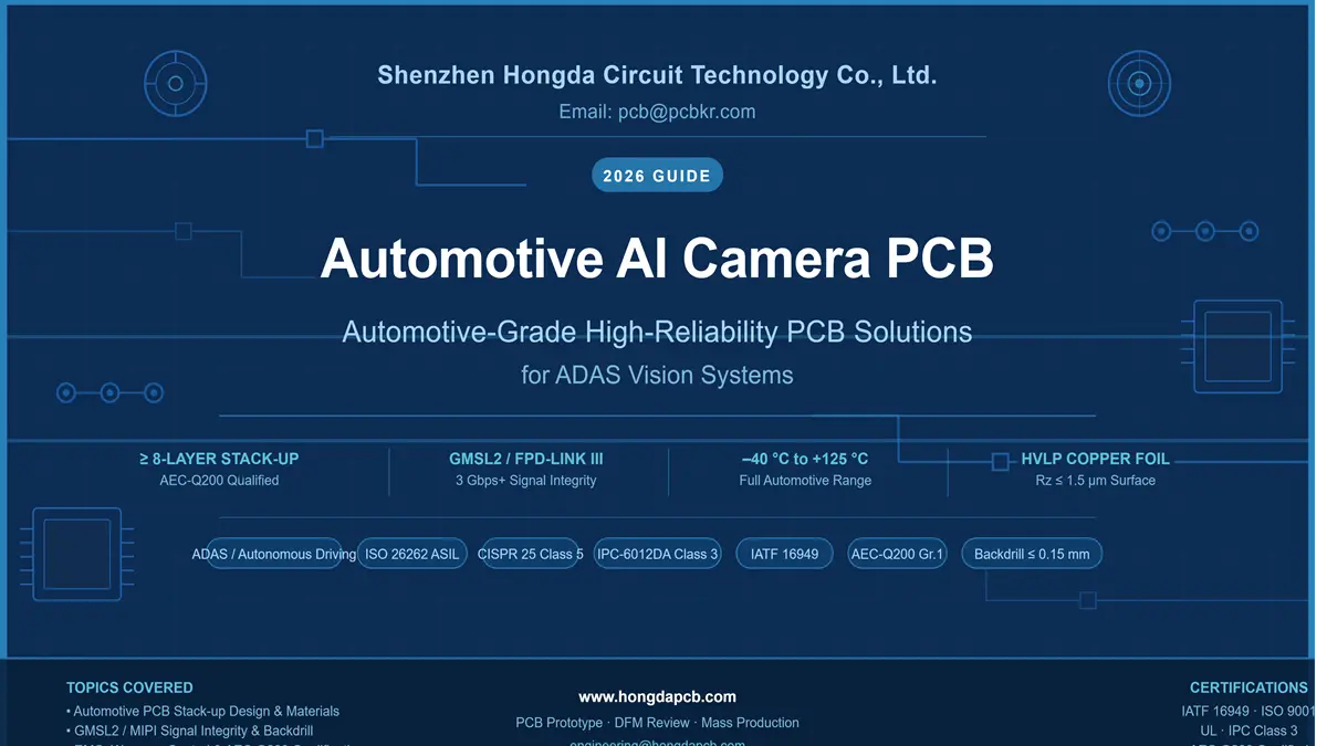
Automotive AI Camera PCB Manufacturing: ADAS Design, Stackup and OEM Requirements
An automotive AI camera PCB must support the electrical, mechanical, thermal and manufacturing requirements of its specific ADAS camera architecture. For OEMs and Tier-1 suppliers, selecting a PCB manufacturer involves more than checking layer count or comparing unit prices. The supplier must review the released stackup, high-speed interfaces, impedance requirements, HDI structures, fabrication tolerances, inspection scope and production documentation.
Shenzhen Hongda Circuit Technology Co., Ltd. (PCBKR) provides custom multilayer PCB fabrication and PCBA assembly for OEM projects. Our manufacturing review can address customer-defined high-speed routing, fine-line structures, microvias, electrical testing and assembly requirements. Each automotive camera project is evaluated against its actual Gerber or ODB++ data, stackup, material specification, BOM and acceptance criteria. Send your project files to sales@pcbkr.com for an engineering and quotation review.
1. What Makes an Automotive AI Camera PCB Different from an Industrial Camera PCB?
Automotive AI camera PCBs are designed for camera systems operating within a vehicle environment. Their requirements depend on the camera’s position, image sensor, serializer and deserializer architecture, power arrangement, connector system, enclosure and vehicle-level validation plan.
An automotive front camera, surround-view camera, driver monitoring camera and rear-view camera may use different electronic architectures. Their PCB designs should therefore not be treated as interchangeable.
| Design factor | Automotive AI camera | Industrial machine vision camera |
|---|---|---|
| Main application | ADAS, surround view, driver monitoring, parking assistance | Inspection, measurement, robotics and factory automation |
| Operating environment | Vehicle temperature, vibration, humidity and mechanical constraints | Factory temperature, vibration, dust and equipment-specific conditions |
| Video connection | MIPI CSI-2 within the module, or automotive SerDes links such as GMSL or FPD-Link | GigE Vision, USB3 Vision, CoaXPress or other industrial interfaces |
| Mechanical constraints | Compact enclosure, vehicle mounting, connector and cable interface | Camera housing, lens alignment, mounting and industrial cable interface |
| Reliability requirements | Defined by the automotive program and applicable component/system requirements | Defined by the machine builder and industrial application |
| Manufacturing documentation | Customer-defined revision, inspection, traceability and qualification records | Project-specific manufacturing and quality records |
A useful distinction is that an automotive camera PCB is one part of a larger electronic and mechanical system. The PCB manufacturer is responsible for building the board to the released fabrication requirements. The camera-module and vehicle development teams remain responsible for system integration and the applicable product-level validation.
2. Which PCB Architectures Are Used in Automotive ADAS Camera Modules?
The PCB architecture depends on where image processing takes place and how video data travels from the camera sensor to the vehicle computing system.
Two common design approaches are a local camera-processing architecture and a remote-processing architecture using automotive SerDes.
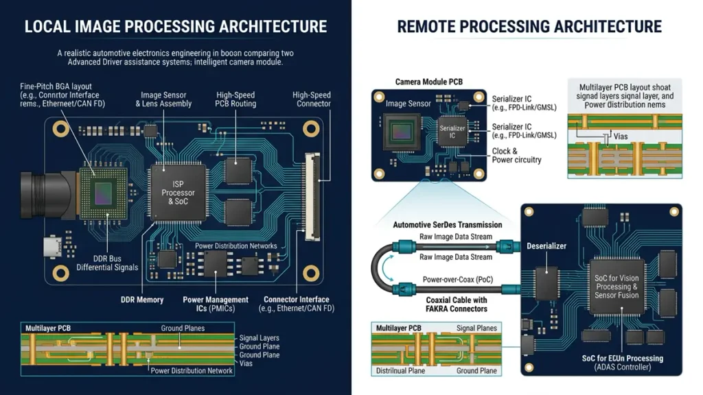
Automotive AI camera PCB architectures for local processing and remote SerDes
Local image processing on the camera board
A camera module may include an image sensor, power-management circuitry and an image signal processor (ISP) or other processing device.
Depending on the design, the PCB may need to accommodate:
- Image sensor connections and associated high-speed signal routing.
- ISP or processor interfaces.
- Memory and supporting components, where required.
- Multiple regulated power rails.
- Clock, reset and control signals.
- Thermal paths and mechanical mounting requirements.
The presence of an ISP or processor can increase component density, routing complexity and thermal-management requirements. Fine-pitch BGA packages may also require a more detailed fanout and via design review.
Remote processing through automotive SerDes
In a satellite-camera architecture, the camera module may contain the image sensor, serializer and power-management circuitry, while image processing takes place in a central ECU or domain controller.
The board may need to support:
- Image sensor to serializer connectivity.
- Serializer power and clock requirements.
- Coaxial or other specified high-speed connector interfaces.
- Power-over-coax (PoC), if included in the design.
- Bidirectional control and diagnostic signals.
- Protection, filtering and power-conditioning circuits.
This architecture changes the PCB’s signal-routing and power-distribution requirements. The connector launch, serializer interface, reference-plane continuity and power-filter layout need to be considered together.
What should buyers confirm before requesting a quotation?
Before choosing a PCB layer count, provide the manufacturer with:
- Image sensor and serializer/deserializer part numbers.
- Whether image processing is local or remote.
- The interface topology and lane configuration.
- Connector type and cable arrangement.
- Power input, PoC and voltage-rail requirements.
- Board outline, thickness and mechanical constraints.
- The required PCB fabrication and PCBA scope.
Do not select an eight-layer or other fixed layer count simply because it appears in a reference design. The correct construction depends on the actual circuit, routing density, electrical targets and mechanical package.
3. How Do GMSL2, FPD-Link III and MIPI CSI-2 Affect PCB Design?
GMSL2, FPD-Link III and MIPI CSI-2 are not interchangeable PCB routing requirements. They describe different parts of a camera data architecture and must be evaluated against the selected component documentation.
GMSL2 camera PCB design
GMSL2 is used in automotive camera and other high-speed video-link applications. Its PCB implementation may involve a serializer or deserializer, a coaxial or other supported interconnect, AC-coupling components and control-channel connections.
For the PCB manufacturer, important review items include:
- Differential or other specified signal geometry at the relevant device interfaces.
- Reference-plane continuity along critical signal routes.
- Connector and cable launch geometry.
- Via transitions and possible impedance discontinuities.
- Component placement around coupling and protection circuits.
- The stackup and dielectric construction used for impedance calculation.
The actual impedance, routing and channel requirements must come from the selected device documentation and customer design specification. A generic trace width or spacing should not be copied from another GMSL2 design.
FPD-Link III camera PCB design
FPD-Link III is another automotive SerDes technology used to transfer camera data and related signals. Some implementations support power-over-coax and bidirectional communication over the specified interconnect.
The PCB design should account for:
- Serializer and deserializer device recommendations.
- The selected cable and connector interface.
- AC-coupling and filtering requirements.
- PoC power-injection and separation circuitry, when applicable.
- Ground return paths and connector transitions.
- The electrical limits specified by the component manufacturer.
The PCB fabricator can review the manufacturability of the supplied layout and stackup. System-level link performance still depends on the complete channel, including components, connectors, cable and receiver.
MIPI CSI-2 camera PCB design
MIPI CSI-2 commonly connects an image sensor to an ISP or processor within a camera module or electronic system.
The PCB design should consider:
- Lane configuration and clocking.
- Differential-pair geometry.
- Reference-plane continuity.
- Pair-to-pair and intra-pair routing requirements.
- Connector or flex transitions, if present.
- Sensor and processor placement.
- Power integrity and noise coupling.
MIPI CSI-2 requirements depend on the selected devices and implementation. The manufacturer should work from the released design rules rather than assume a universal impedance, length-matching or layer arrangement.
Interface and manufacturing review checklist
| Interface or function | Information required from the OEM | PCB manufacturing review |
|---|---|---|
| GMSL2 | Device data sheets, topology, channel and connector details | Stackup, routing geometry, transitions and fabrication feasibility |
| FPD-Link III | Serializer/deserializer data, cable interface and PoC requirements | Layer structure, connector area, drilling and power-circuit layout |
| MIPI CSI-2 | Sensor and processor data sheets, lane configuration and routing rules | Fine-pitch routing, reference planes, via transitions and impedance requirements |
| Camera power | Input voltage, rail sequence, current and filtering requirements | Copper distribution, clearances and board construction |
| Control and diagnostics | I²C, SPI, UART, reset and diagnostic requirements | Routing separation, test access and assembly details |
4. What PCB Stackup and Materials Should OEMs Specify for Automotive Cameras?
The stackup should be treated as a controlled electrical and manufacturing specification. Layer count alone does not determine whether a PCB can support a camera interface.
A practical stackup review should include the laminate grade, dielectric thickness, copper construction, reference-plane arrangement, controlled-impedance nets and finished board thickness.
How should OEMs select PCB materials?
Material selection should be based on the operating conditions and electrical requirements of the actual design.
| Material consideration | Engineering question | What the manufacturer needs |
|---|---|---|
| Standard FR-4 | Does the design meet its electrical and thermal requirements with the selected grade? | Exact laminate grade and manufacturer data sheet |
| High-Tg FR-4 | Does the assembly or operating environment require a higher-temperature material? | Tg, Td and applicable material specification |
| Low-loss laminate | Does the signal channel require lower dielectric loss or a particular Dk range? | Frequency-dependent Dk/Df requirements and approved material list |
| Copper foil | Does the design require a particular copper type or roughness? | Copper foil specification and layer assignment |
| Resin and dielectric construction | Can the pressed dielectric thickness support the target impedance and finished board thickness? | Stackup drawing and dielectric requirements |
| Material substitution | Are alternative grades permitted? | Approved material list and written change-control rules |
A material should not be selected solely because it is marketed as automotive grade. The specific laminate data sheet, electrical requirements, thermal conditions and customer approval process should guide the decision.
What should an automotive camera PCB stackup drawing include?
A complete stackup package should identify:
- Total layer count and layer sequence.
- Signal, ground and power layer functions.
- Core and prepreg material grades.
- Dielectric thicknesses.
- Starting and finished copper thickness requirements.
- Controlled-impedance layers and nets.
- Finished board thickness and tolerance.
- Surface finish and solder-mask requirements.
- Any blind, buried or microvia structures.
- Approved alternatives and material restrictions.
Illustrative four-layer stackup concept
The following is an educational example, not a recommended universal automotive camera stackup or a fabrication-ready construction.
| Layer | Typical function |
|---|---|
| L1 | Components and signal routing |
| L2 | Continuous ground reference plane |
| L3 | Power distribution and secondary signals, as appropriate |
| L4 | Components and signal routing |
A four-layer construction may be suitable for some relatively simple camera boards. Designs with denser BGA packages, multiple high-speed interfaces, more complex power distribution or tighter mechanical constraints may require additional layers or HDI structures.
The final layer arrangement must be reviewed against the actual design.
5. When Does an Automotive Camera PCB Need HDI, BGA Fanout or Microvias?
HDI technology may be required when the camera PCB has limited physical area, dense component placement or fine-pitch package connections that are difficult to route using conventional through-hole vias.
Common design considerations include:
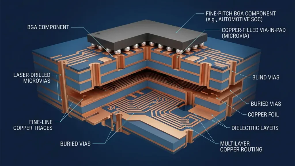
Automotive AI camera PCB HDI microvias and BGA fanout structure
- Fine-pitch image sensor or processor packages.
- BGA fanout and escape routing.
- Compact serializer and power-management layouts.
- Blind and buried via structures.
- Microvia-in-pad or via-in-pad designs, where specified.
- High routing density around connectors and component areas.
BGA fanout and via-in-pad considerations
BGA fanout should be reviewed before the PCB enters fabrication. The design must account for pad geometry, solder-mask definition, via position, via filling or capping requirements and the assembly process.
A via-in-pad structure should not be assumed to be suitable simply because it saves routing space. Its manufacturing method and surface condition need to be defined, especially when the pad is used for fine-pitch soldering.
PCBKR’s relevant manufacturing capabilities
PCBKR has documented manufacturing processes that may be relevant to dense camera-board designs:
| Process or equipment | Documented capability |
|---|---|
| SCREEN Ledia LDI | 8 µm fine-line imaging target; ±10 µm process registration target |
| mSAP | 8/8 µm line/space process capability, in place since Q3 2024 |
| Mitsubishi UV/CO₂ laser | 75 µm microvia capability with ±5 µm process capability |
| Picosecond laser | 50 µm processing capability |
| LAUFFER lamination | Documented pressure settings of 80, 150 and 200 psi; vacuum below 50 mbar |
These figures describe documented process capabilities, not guaranteed finished-board specifications for every automotive camera design. Actual feasibility depends on copper thickness, material, layer count, via structure, board dimensions and the released fabrication data.
For additional information about high-density interconnection, see HDI PCB manufacturing.
6. How Should Signal Integrity and Controlled Impedance Be Reviewed?
High-speed camera links require the electrical design and physical PCB construction to agree. A target impedance written on a drawing is not sufficient if the stackup, copper geometry and manufacturing assumptions have not been reviewed.
What affects PCB impedance?
Important factors include:
- Trace width and spacing.
- Finished copper thickness.
- Dielectric thickness between the signal and reference layers.
- Laminate dielectric properties.
- Copper foil profile and surface roughness.
- Solder-mask effects on outer-layer traces.
- Routing geometry and via transitions.
- Reference-plane continuity.
A change to any of these variables may affect the resulting impedance. Therefore, the PCB manufacturer should review the proposed stackup before production rather than simply use a generic trace-width calculator.
What should the OEM include in the impedance specification?
The fabrication drawing or impedance table should identify:
- Single-ended and differential target impedances.
- The relevant signal nets and routing layers.
- The required tolerance.
- The stackup revision used for calculation.
- The required coupon arrangement, if applicable.
- The requested measurement method and report format.
- The approval process for any geometry or stackup change.
The target and tolerance must be agreed upon for the particular design. Do not assume that every automotive camera PCB requires the same impedance value or tolerance.
For more information about impedance-related manufacturing considerations, see PCBKR’s PCB impedance control service.
How should TDR verification be specified?
Time-domain reflectometry (TDR) can be used to evaluate the characteristic impedance of an appropriate test structure. For a controlled-impedance PCB project, the OEM and manufacturer should agree on:
- Coupon design and location.
- The impedance target and tolerance.
- Test access and measurement setup.
- The number of samples or panels to be measured.
- The acceptance criteria.
- The report and traceability requirements.
A coupon result represents the tested structure under the specified measurement conditions. It does not automatically prove the electrical performance of every component, connector, cable or assembled camera module.
PCBKR has project-specific TDR and impedance verification experience. Measurement scope and reporting should be confirmed during engineering review and quotation. The company also has VNA capability up to 70 GHz; whether VNA testing is appropriate depends on the project and the agreed test method.
7. How Can PCB Manufacturers Help Control EMI, Power Integrity and Thermal Risks?
An automotive camera PCB can contain sensitive image-sensor signals, high-speed SerDes interfaces, switching power circuits, clocks and control signals in a compact area.
These circuits can interact through shared power paths, reference planes, parasitic coupling and mechanical constraints.
EMI and return-path review
A manufacturing and design review should consider:
- Continuous reference planes beneath critical high-speed routes.
- Return-current paths at layer transitions.
- Separation of sensitive analog and noisy switching circuits.
- Grounding and stitching-via arrangements where specified.
- Connector and cable launch geometry.
- Placement of filters and protection components.
- The relationship between board layout and enclosure shielding.
Avoid treating a via fence or ground-plane split as a universal EMI solution. Its effectiveness depends on the frequency, geometry, current path and complete system design.
Power integrity
Camera modules may contain several supply rails for image sensors, serializers, processors and supporting circuits.
The OEM should provide:
- Input-voltage range.
- Required output rails and tolerances.
- Startup and shutdown sequence.
- Expected current and transient loads.
- Power-over-coax requirements, where applicable.
- Filtering and noise limits.
- Test points and measurement requirements.
The PCB manufacturer can review copper distribution, clearance, manufacturability and assembly constraints. Power sequencing and circuit performance must be verified against the customer’s electrical test requirements.
Thermal management
Thermal requirements depend on component power dissipation, board dimensions, enclosure design, mounting, airflow and the vehicle’s operating environment.
Potential design measures include:
- Appropriate copper distribution.
- Thermal vias where required by the design.
- Component placement that supports the intended heat path.
- Thermal pads or interfaces specified by the customer.
- Suitable laminate and assembly materials.
- Mechanical coordination with the camera housing.
A PCB material’s Tg alone does not establish the maximum operating temperature of a complete camera module. The OEM should define the operating and storage conditions and identify the tests required for product qualification.
8. What Reliability and Quality Tests Should Buyers Define?
Automotive camera qualification is a system of requirements. The PCB, PCBA, camera module, cable and vehicle may each have different verification responsibilities.
The buyer should identify which tests apply to the bare PCB, which apply after assembly and which must be performed at the module or vehicle level.
| Verification activity | Main purpose | Scope and limitation |
|---|---|---|
| Bare-board electrical test | Checks specified electrical connectivity on the fabricated PCB | Does not verify assembled-board function |
| Visual inspection | Identifies visible manufacturing defects | Cannot detect every internal or concealed defect |
| 3D AOI | Inspects visible assembly features within the system’s inspection capability | Does not replace electrical or functional testing |
| X-ray inspection | Examines selected concealed solder joints, including appropriate BGA packages | Coverage and acceptance criteria must be defined |
| Four-wire Kelvin measurement | Measures low resistance with reduced influence from test-lead resistance | Only applicable to defined measurement points and test conditions |
| TDR | Evaluates impedance on suitable test structures | Does not qualify the complete camera channel |
| VNA measurement | Evaluates frequency-domain characteristics of a suitable test structure or channel | Requires a defined fixture, calibration and test plan |
| Functional testing | Checks specified electrical and communication functions | Requires an agreed test procedure and pass/fail limits |
| Environmental testing | Evaluates defined temperature, humidity, vibration or other stresses | Must be assigned to the responsible supplier or test laboratory |
Which automotive standards should be considered?
The standards and specifications depend on the product, component and customer quality plan.
- AEC-Q100 applies to qualification of integrated circuits and other relevant active electronic components.
- AEC-Q200 applies to qualification of relevant passive electronic components.
- ISO 16750 provides environmental conditions and testing considerations for electrical and electronic equipment in road vehicles.
- CISPR 25 addresses radio-disturbance characteristics and limits for vehicle components and modules.
- ISO 26262 addresses functional safety of road vehicles’ electrical and electronic systems.
- IPC-6012 may be specified for rigid printed board qualification and acceptance, with the applicable revision and class agreed by the customer.
These standards do not mean that a bare PCB automatically receives AEC-Q100, AEC-Q200 or ASIL certification. Buyers should identify the applicable standard, product level, test owner, sample plan and acceptance criteria in the project specification.
What inspection records should the supplier provide?
Depending on the order scope, buyers may request:
- Fabrication inspection records.
- Electrical test results.
- Material certificates or certificates of conformance, where specified.
- Stackup and impedance reports, where required.
- AOI or X-ray inspection records for assembled boards.
- Nonconformance and corrective-action records.
- Approved revision and production-lot information.
The quotation should state which records are included and which require additional testing, fixtures or third-party services.
9. How Should OEMs Qualify an Automotive AI Camera PCB Manufacturer?
A supplier qualification review should establish whether the manufacturer can build the customer’s actual PCB construction and provide the required evidence.
A website capability list is only a starting point. The buyer should confirm that the processes, equipment and inspection methods are applicable to the proposed design.
Automotive camera PCB supplier audit checklist
| Audit area | Questions for the supplier | Evidence to request |
|---|---|---|
| Engineering review | Can the supplier review Gerber/ODB++, stackup and fabrication notes? | DFM comments and engineering clarification records |
| Material control | Can the specified laminate grade be used and controlled? | Material identification and applicable certificates |
| Stackup management | Will the supplier confirm dielectric and copper construction before fabrication? | Approved stackup and revision record |
| Impedance control | Can the supplier review specified impedance nets and test coupons? | Agreed impedance plan and applicable measurement report |
| HDI manufacturing | Can the supplier manufacture the specified microvia and BGA fanout structure? | Process capability review and relevant inspection evidence |
| Bare-board testing | Which electrical tests are included? | Electrical test method and result records |
| PCBA assembly | Can the supplier perform the required SMT or THT assembly? | Agreed assembly scope and inspection plan |
| BGA inspection | Is X-ray inspection available where required? | Defined X-ray coverage and acceptance criteria |
| Change control | How are material, stackup, process and revision changes handled? | Written change notification and approval process |
| Traceability | What production and material records can be linked to the order? | Confirmed traceability scope |
| Nonconformance | How are defects isolated and corrective actions documented? | Nonconformance and corrective-action procedure |
Questions to ask before approving a new supplier
- Can you manufacture the exact layer count, finished thickness and copper construction in our released drawing?
- Can you review the stackup against our controlled-impedance requirements?
- How are proposed trace-width or dielectric-thickness changes submitted for approval?
- Which microvia structures and BGA fanout methods are feasible for our design?
- What bare-board electrical test coverage is included?
- Can you provide TDR results or other specified electrical evidence?
- Which PCBA inspection processes are included in the quotation?
- How do you control material substitutions and production revisions?
- Which records can be supplied for each production lot?
- What is excluded from the quoted price and delivery schedule?
10. How Can Buyers Control Prototype-to-Production Transfer?
A camera PCB that works during an initial prototype evaluation is not automatically ready for repeat production.
The transition should control the design revision, stackup, material, component sourcing, assembly process, inspection plan and functional test requirements.
A practical transfer process includes the following stages.
Stage 1: Confirm the released design package
The buyer should confirm that the following files match:
- PCB fabrication data.
- Stackup drawing.
- Fabrication notes.
- BOM and approved manufacturer part numbers.
- Pick-and-place data.
- Assembly drawings.
- Test instructions.
- Mechanical drawing and board outline.
Stage 2: Complete the engineering review
Resolve questions about:
- Impedance targets and stackup assumptions.
- BGA fanout and via structures.
- Board thickness and mechanical tolerances.
- Material grades and approved alternatives.
- Connector and cable interfaces.
- Assembly clearances and inspection access.
Any proposed manufacturing change should be documented and approved before production.
Stage 3: Review the prototype or pilot build
The buyer and supplier should evaluate the agreed inspection and test results. Defects should be classified according to whether they originate from the bare PCB, components, assembly, design or test procedure.
Stage 4: Approve the production baseline
Before volume production, confirm:
- Approved PCB and PCBA revisions.
- Approved material and component list.
- Inspection and test coverage.
- Acceptance criteria.
- Required manufacturing records.
- Change-control responsibilities.
Stage 5: Control subsequent changes
Changes to laminate, copper construction, stackup, components, manufacturing location, assembly process or test method may affect product performance and qualification.
The OEM should define which changes require notification, engineering review or written customer approval.
This is especially important when a supplier proposes an alternative material or modifies impedance-related geometry to improve manufacturability. A supplier should not silently substitute a material or change a critical trace dimension after design approval.
11. What Determines Automotive Camera PCB Cost and Lead Time?
Automotive camera PCB pricing depends on the actual construction and production scope. A small board can still be expensive to manufacture if it requires dense BGA routing, special materials, HDI structures, controlled impedance or extensive inspection.
| Cost or schedule factor | Why it matters | What buyers should provide |
|---|---|---|
| Layer count | Affects material usage and lamination complexity | Released layer stackup |
| Board dimensions | Influences panel utilization and manufacturing yield | Board outline and quantity |
| Material grade | Specialty laminates may affect material cost and process planning | Approved laminate grade and alternatives |
| Copper construction | Affects etching, plating and trace geometry | Starting and finished copper requirements |
| HDI structures | May require laser drilling and sequential lamination | Via structure and microvia drawings |
| Impedance requirements | Requires stackup review and potentially test coupons | Target impedance, tolerance and net list |
| Surface finish | Depends on component pitch, solderability and customer requirements | Specified finish and acceptance requirements |
| Assembly complexity | BGA, fine-pitch packages and mixed technology affect assembly effort | BOM, placement data and assembly drawing |
| Inspection and testing | Additional coverage may require fixtures, engineering and reporting | Inspection and test plan |
| Component availability | Long-lead-time parts can delay PCBA delivery | Complete BOM and approved alternatives |
How can procurement compare quotations accurately?
Ask each supplier to quote against the same:
- PCB revision and manufacturing files.
- Stackup and material specification.
- Board quantity and delivery schedule.
- Surface finish and copper requirements.
- Impedance and test requirements.
- BOM and component sourcing scope.
- Assembly and inspection coverage.
- Packaging, shipping and documentation requirements.
A lower bare-board price may not include the same test coupons, inspection records, assembly services or traceability as another quotation. Compare the complete scope before selecting a supplier.
12. What Should Buyers Include in an Automotive Camera PCB RFQ?
A complete RFQ helps the supplier identify manufacturing risks and quote the correct construction rather than making assumptions.
PCB fabrication files
Provide:
- Gerber or ODB++ files.
- NC drill files.
- Stackup drawing.
- Board outline and dimensions.
- Finished thickness and tolerance.
- Copper thickness requirements.
- Material grade and approved alternatives.
- Surface finish and solder-mask requirements.
- Impedance targets, controlled-net list and tolerances.
- HDI, blind/buried via and microvia details.
- Applicable fabrication and acceptance standards.
PCBA files, if assembly is required
Provide:
- BOM with manufacturer part numbers.
- Pick-and-place or centroid file.
- Assembly drawings.
- Component polarity and orientation details.
- BGA and fine-pitch package requirements.
- Approved or prohibited component substitutions.
- Programming instructions, if required.
- Functional test procedure and acceptance limits, if required.
Commercial and quality information
Also specify:
- Prototype and production quantities.
- Expected repeat-order volumes.
- Required delivery date.
- Delivery destination.
- Packaging requirements.
- Lot or serial-number traceability requirements.
- Required inspection and test reports.
- Customer approval and change-control requirements.
If the camera module has a specific GMSL2, FPD-Link III or MIPI CSI-2 implementation, include the relevant component documentation and interface requirements. This allows the engineering team to review the actual design instead of relying on generic assumptions.
13. Automotive AI Camera PCB Manufacturing and PCBA Support from PCBKR
Shenzhen Hongda Circuit Technology Co., Ltd. provides custom PCB fabrication and PCBA assembly for OEM projects. For automotive camera-related designs, the manufacturing scope is evaluated against the customer-approved files and requirements.
Relevant manufacturing resources include:
- Multilayer PCB fabrication and stackup review.
- Fine-line imaging using SCREEN Ledia LDI equipment.
- mSAP 8/8 µm line/space process capability.
- Laser microvia processing.
- LAUFFER vacuum lamination.
- 3D AOI and X-ray inspection.
- Four-wire Kelvin measurement.
- Project-specific impedance and TDR verification.
- VNA measurement capability up to 70 GHz.
The applicable process, inspection and test scope depends on the design and quotation. Automotive-specific qualification tests, module-level validation, EMC testing, environmental testing, firmware programming and functional testing should be identified separately and confirmed before order placement.
For a broader overview of PCBKR’s manufacturing resources, see the PCB manufacturing capability page.
Request an Automotive AI Camera PCB Quotation
To request a manufacturing review, send the available Gerber or ODB++ files, stackup, BOM, board quantity and required inspection or test specifications.
Shenzhen Hongda Circuit Technology Co., Ltd.
Email: sales@pcbkr.com
Website: https://www.pcbkr.com
PCBKR can review the supplied project information, clarify manufacturing questions and confirm the appropriate PCB fabrication and PCBA assembly scope before quotation.
Frequently Asked Questions About Automotive AI Camera PCBs
What is an automotive AI camera PCB?
An automotive AI camera PCB is the circuit board used in an automotive camera module or related camera electronics. It may connect an image sensor, serializer, power-management circuitry, ISP or processor, depending on the camera architecture. Its manufacturing requirements depend on the electrical interfaces, mechanical design and vehicle-program specifications.
What PCB materials are used for automotive camera modules?
Material selection depends on operating temperature, electrical loss, dielectric properties, thermal expansion, moisture requirements and the customer’s approved material list. Standard FR-4, high-Tg FR-4 or low-loss laminates may be considered according to the actual design. The exact laminate grade should be identified rather than specified only by a generic material category.
Does a GMSL2 or FPD-Link III camera PCB need controlled impedance?
The relevant high-speed signal paths must follow the electrical requirements of the selected serializer, deserializer, connector and channel design. Where controlled impedance is specified, the stackup, dielectric thickness, copper geometry, reference plane and test method should be agreed before fabrication. The exact impedance value and tolerance are project-specific.
How many layers does an automotive AI camera PCB need?
There is no universal layer count. A relatively simple camera board may use a four-layer construction, while denser designs with BGA packages, multiple interfaces, complex power distribution or HDI routing may need more layers. The final layer count should be determined by the routing, electrical, thermal and mechanical requirements.
When should an automotive camera PCB use HDI and microvias?
HDI and microvias may be appropriate when a compact board needs fine-pitch BGA fanout, higher routing density or shorter interconnections. Their use should be confirmed through a review of the package pitch, via design, stackup, material and manufacturing process.
How is impedance verified on an automotive camera PCB?
A suitable test coupon can be measured using TDR when the project specification requires it. The OEM and manufacturer should agree on coupon design, target impedance, tolerance, sample plan and reporting. Coupon results do not by themselves qualify the complete camera module, cable or vehicle-level channel.
Does an automotive camera PCB need AEC-Q100 or ASIL-D certification?
AEC-Q100 is used for qualification of applicable integrated circuits, not as a certification for bare PCBs. ASIL-D is a functional-safety level within the ISO 26262 framework for relevant automotive systems and development processes. The OEM should identify the applicable component, board, module and system-level requirements rather than assume that the PCB itself receives these certifications.
What should an OEM send to an automotive camera PCB manufacturer for a quotation?
Provide Gerber or ODB++ files, drill data, stackup, material grade, copper requirements, board dimensions, impedance specifications, BOM, assembly drawings, order quantity and required inspection or testing criteria. For GMSL2, FPD-Link III or MIPI CSI-2 designs, include the relevant device documentation and interface requirements so the manufacturer can review the actual construction and production scope.
About Author
David Chen LinkedIn Profile
David Chen is a Senior RF/PCB Process Engineer at Shenzhen Hongda Circuit Technology Co., Ltd., with over 12 years of experience in high-frequency PCB fabrication, impedance-controlled stack-up design, and Rogers/PTFE laminate processing. He also boasts an extensive professional background in PCBA manufacturing, PCBA testing, and PCBA optimization, with specialized expertise in high-precision PCBA fault analysis and rigorous PCBA reliability testing. The author has worked with high-layer-count server PCB fabrication, ultra-low-loss backplane stackups, and thermo-mechanical reliability optimization for AI infrastructure projects involving 112G and 224G PAM4 architectures. Skilled in complex circuit design and cutting-edge advanced PCB manufacturing processes, he delivers solutions that elevate product durability and performance across industrial applications. His technical articles focusing on PCBA manufacturing workflows and testing methodologies are widely cited by industry peers and technical platforms, and have gained attention and recognition from industry colleagues.