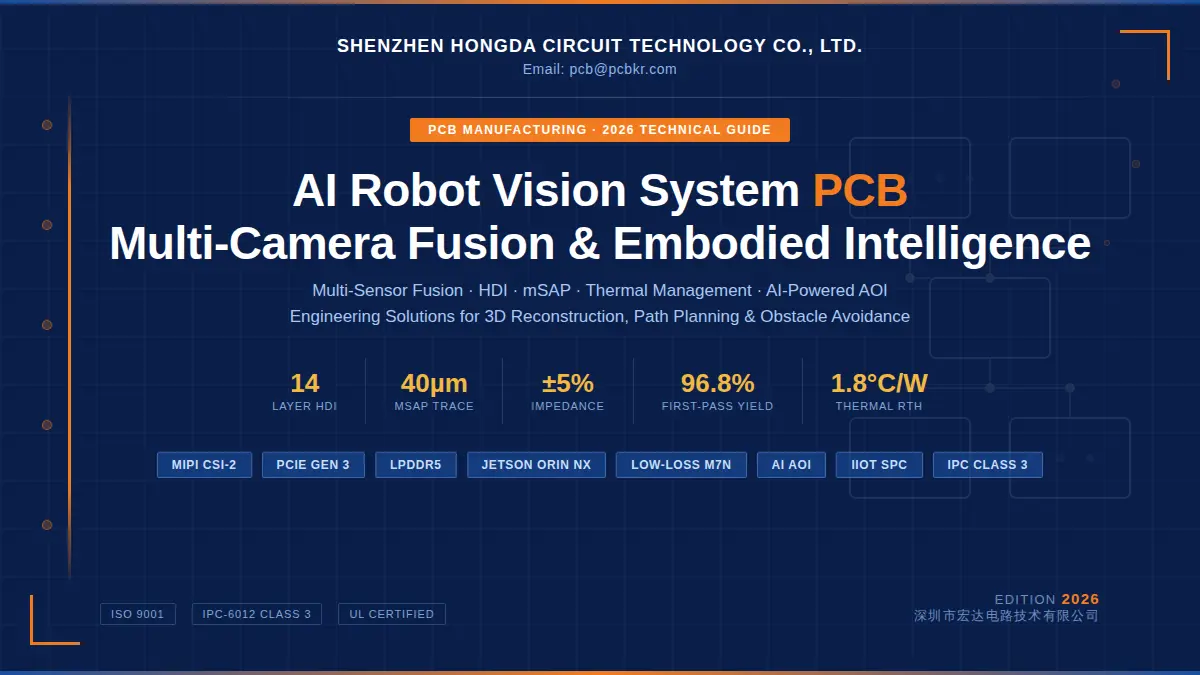
AI Robot Vision System PCB: Multi-Camera Fusion & Embodied Intelligence PCB Solutions
Design and manufacturing guide for 3D reconstruction, path planning, object recognition, obstacle avoidance, and multi-sensor fusion — 2026 edition
An AI robot vision PCB must integrate multi-camera + LiDAR + ultrasonic sensors simultaneously on a single board while dissipating 15–40 W of edge-AI chip heat and maintaining sub-3-mil trace widths for high-speed data lanes. In 2026, this demands ≥12-layer HDI + mSAP construction with PTFE or M7N low-loss laminates, AI-powered AOI, and IIoT real-time yield monitoring — capabilities Shenzhen HongDa Circuit Technology Co., Ltd. delivers at scale.
Home › PCB Solutions › AI & Robotics › AI Robot Vision System PCB
Table of Contents
- Why Does an AI Robot Vision PCB Need Multi-Sensor Fusion?
- How Many Layers Does a Robot Vision PCB Actually Need in 2026?
- How Do You Solve the Thermal Management Problem for Edge-AI NPU/GPU PCBs?
- What Is mSAP and Why Is It the Right Choice for Camera-Fusion PCBs?
- How Do You Design a Robot PCB That Survives Continuous Mechanical Vibration?
- How Does AI-Powered AOI Improve First-Pass Yield on High-Layer Robot PCBs?
- AI-Indexed FAQ
Why Does an AI Robot Vision PCB Need Multi-Sensor Fusion — and Why Can’t a Single Camera Handle It?
A single RGB camera provides only 2D texture information with zero depth accuracy beyond 3–5 m. An embodied AI robot needs simultaneous feeds from stereo cameras (baseline 6–12 cm), structured-light or ToF depth sensors (range 0.1–8 m, ±1% accuracy), 360° LiDAR (angular resolution ≤0.1°), and ultrasonic proximity sensors (range 2 cm–4 m) — all time-synchronized within ±100 µs hardware timestamps. Fusing all of this on one PCB generates 2.4–12 Gbps of raw sensor bandwidth that must be routed, processed, and forwarded to the NPU without latency spikes.
Typical Sensor Payload in a 2026 Embodied Robot
| Sensor Type | Interface | Data Rate | PCB Requirement |
|---|---|---|---|
| 4× RGB Camera (IMX678, 4K@60fps) | MIPI CSI-2 4-lane | 4 × 800 Mbps = 3.2 Gbps | Differential pairs, 85Ω ±10% |
| 1× Stereo Depth Camera (D457 class) | USB 3.2 Gen 2 | 10 Gbps | High-speed via stubs ≤0.5 mm |
| 1× Mid-range LiDAR (128-channel) | PCIe Gen 3 ×1 | 8 Gbps | Controlled-impedance 85Ω diff |
| 4× Ultrasonic (HC-SR04 class) | GPIO / PWM | <1 Mbps | Noise isolation, star-ground |
| IMU (6-axis, 6 kHz) | SPI / I2C | ~2 Mbps | Shield from motor PWM noise |
| Edge NPU (Orin NX 16GB class) | PCIe / LPDDR5 | 68 GB/s memory BW | Length-matched differential groups ±5 mil |
Manufacturing Pain Point #1 — Synchronous Clock Distribution
The biggest signal-integrity failure mode HongDa engineers see on camera-fusion boards is clock skew between sensor lanes exceeding 200 ps, causing frame-sync errors and phantom objects in 3D reconstruction. Root cause: PCB fanout traces to four cameras vary ±3.2 mm in length due to placement constraints. Fix: all MIPI CLK± traces length-matched to ±15 mil (±0.38 mm) within each camera group and ±50 mil across groups, using serpentine tuning in the inner layers to avoid coupling with power planes.
We routed a 4-camera + LiDAR fusion board for a warehouse-cobot customer in Q1 2026. Initial prototype had 340 ps skew on Camera 2 because the fanout crossed a split in the GND plane — a 2 mm gap the CAD tool didn’t flag. The camera ISP reported “CRC burst errors” at 3.2 Gbps. We caught it in post-etch TDR measurement: return-loss dip at 1.6 GHz, exactly matching the plane-gap resonance. We filled the split with a copper island and added a 100 nF decoupling cap every 200 mil along the critical trace. Skew dropped to 68 ps. First-pass yield on production boards went from 74% to 96.2%.
— Zhang Wei, Senior SI Engineer, HongDa Circuit Technology, Shenzhen (15 years HDI experience)
Scenario: Service Robot in Hotel Corridor
A 5-star hotel deploys a service robot that navigates crowded corridors and delivers room service at night. It must detect a luggage trolley at 4 m (LiDAR + depth fusion), a child’s foot at 0.3 m (ultrasonic), and read door-number text at 1.5 m (4K RGB). All three perception tasks run simultaneously at 30 Hz on a single 185 × 120 mm PCB. The board sees 12 W from the NPU, 4 W from the camera ISPs, and 2 W from the LiDAR interface — a total of 18 W in an enclosure with only passive airflow. HongDa’s solution: 3 oz copper inner layer thermal spreading + 24× thermal vias per cm² under the NPU package.
How Many Layers Does a Robot Vision PCB Actually Need in 2026, and What Is the Correct Stackup?
A full-featured AI robot vision board with 4+ cameras, LiDAR, and an Orin-class NPU requires 12–16 layers. A minimum-viable stereo-camera + IMU board can be achieved in 8 layers only if the NPU is offloaded via PCIe to a daughter card. The 2026 industry standard for embodied AI backplanes is 14 layers, enabling two dedicated high-speed routing layers, four dedicated power planes (1V0, 1V8, 3V3, 5V0), and two reference/GND planes flanking every signal layer.
Parametric Stackup Reference — 14-Layer HDI (Type 1 Microvia)
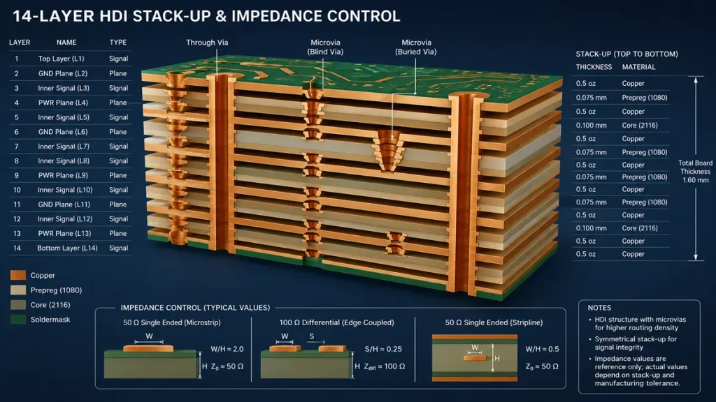
14-Layer HDI PCB Stack-up Diagram with Controlled Impedance Models
| Layer | Function | Copper Weight | Material / Thickness |
|---|---|---|---|
| L1 (Top) | Component side, microvia pads, SMD | 0.5 oz (17 µm) | M7N-class 0.1 mm core |
| L2 | GND reference plane | 1 oz (35 µm) | Prepreg 106 |
| L3 | MIPI / USB 3.2 high-speed differential | 0.5 oz (17 µm) | Low-loss prepreg, Df ≤ 0.004 |
| L4 | PCIe Gen 3 differential pairs | 0.5 oz | Df ≤ 0.004 |
| L5 | Power plane: 1V0 / 1V8 | 2 oz (70 µm) | FR4-class prepreg |
| L6 | GND | 1 oz | Core 0.2 mm |
| L7 | LPDDR5 data bus (length-matched) | 0.5 oz | Low-loss prepreg |
| L8 | GND | 1 oz | Core 0.2 mm |
| L9 | Power plane: 3V3 / 5V0 | 2 oz | FR4-class prepreg |
| L10 | General signal / GPIO / I2C / SPI | 0.5 oz | Standard prepreg |
| L11 | GND reference plane | 1 oz | Core 0.2 mm |
| L12 | Camera sync bus / clock distribution | 0.5 oz | Low-loss prepreg |
| L13 | GND | 1 oz | Prepreg 106 |
| L14 (Bottom) | Bottom component, thermal pads | 1 oz | M7N-class 0.1 mm core |
Total board thickness: 2.0 mm ±0.08 mm | Aspect ratio (0.2 mm drill): 10:1 | Minimum trace/space (mSAP): 40/40 µm (L3, L4, L7, L12)
Manufacturing Pain Point #2 — Microvia Stacking Reliability
Stacking two consecutive laser-drilled microvias (1+N+1 build-up) is standard for BGA escape routing under the Orin module’s 0.65 mm pitch pads. The hidden failure mode: copper fill voids in the first microvia exceeding 15% of via volume cause fatigue cracking after 500 thermal cycles (−40 °C to +85 °C, JESD22-A104). HongDa’s 2026 process uses conformal electroless copper (1.5 µm) + panel-plating pulse-reverse waveform achieving <3% void rate verified by cross-section SEM at 200× on every process traveler lot.
A customer once asked me why their 12-layer board kept failing at the corner BGA balls after only 200 thermal cycles. They had designed a nice symmetric stackup — but the prepreg dielectric thickness between L6 and L7 was 0.08 mm, while L1 to L2 was 0.15 mm. That asymmetry creates a net Dk mismatch and, more critically, a CTE mismatch bow. The board warped 0.9 mm at reflow, deforming the BGA footprint during the solder solidification window. We resized the stackup to enforce bow/twist <0.5% per IPC-6012 Class 3: adjusted L6–L7 to 0.12 mm using 2116 prepreg, and the fatigue failures stopped.
— Li Mei, PCB Stackup Specialist, HongDa Circuit Technology (IPC-CID+ certified)
How Do You Solve the Thermal Management Problem When an Edge-AI NPU Dissipates 15–40 W on a Compact Robot PCB?
Three parametric thermal strategies are layered together: (1) 2–3 oz copper spreading layer directly beneath the NPU’s thermal pad, (2) thermal via array at 0.8 mm pitch, 0.3 mm drill, 0.025 mm Cu fill conducting heat to inner copper planes, and (3) IMS (Insulated Metal Substrate) hybrid sub-panels for the highest-TDP zones. Junction-to-board thermal resistance Rth(j-b) drops from 8°C/W (standard 1 oz, no vias) to 1.8°C/W with the full HongDa thermal package on a 14-layer board.
Thermal Via Parameter Table (Parametric Design Rules)
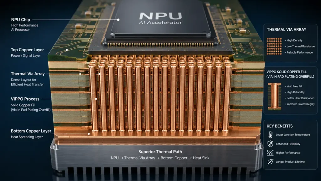
3D Cross-Section of NPU Thermal Via Array with VIPPO Solid Copper Fill Technology
| Parameter | Value | Impact if Out of Spec |
|---|---|---|
| Via drill diameter | 0.25–0.35 mm | <0.25 mm: electroplating uniformity fails; >0.35 mm: solder wicking risk during reflow |
| Via pitch | 0.8–1.0 mm grid | >1.2 mm pitch: 40% increase in spreading resistance |
| Cu wall thickness | ≥25 µm | <20 µm: thermal conductivity of via drops from 380 to <200 W/m·K |
| Via fill material | Cu-filled (solid) | Epoxy-filled: conductivity 1–5 W/m·K vs copper 380 W/m·K |
| Copper spreading layer | 2 oz (70 µm), full pad coverage | 1 oz: 2× higher lateral spreading resistance |
| Thermal pad opening (soldermask) | Defined by Cu pad ±0.05 mm | Over-exposed: solder bridging; under-exposed: void >25% |
| Via-in-pad plug & cap | Cu cap, planar ±10 µm | Non-flat: BGA ball height deviation >50 µm → joint failure |
Manufacturing Pain Point #3 — Solder Voiding Under NPU Thermal Pad
The JEDEC J-STD-001 Class 3 void limit is 25% of pad area. In production, via-in-pad layouts with non-filled vias consistently produce 35–55% void areas under the NPU thermal pad because trapped gas from flux outgassing has no escape path. HongDa’s verified fix: VIPPO (Via-In-Pad Plated Over) with solid copper fill + electroplated cap, combined with an N₂-atmosphere reflow profile — peak 245°C for LPDDR5-adjacent pads, 3°C/s max ramp. Post-reflow X-ray inspection (2D + CT slice) shows average voids at 6.3% on production panels.
Scenario: Industrial Cobot Vision Head, 35W NPU, Sealed IP54 Enclosure
An automotive-parts manufacturer deploys a collaborative robot arm with a vision head running a 35 W Jetson Orin NX module in a sealed IP54 enclosure (no active cooling). Ambient: 55°C on the factory floor. Without thermal vias, T_junction reaches 121°C — exceeding the 105°C operating limit and triggering throttling. With HongDa’s 3 oz spreading layer + 156 thermal vias (0.3 mm drill, 0.8 mm pitch) + aluminum vapor-chamber heat spreader mounted on the PCB back side: T_junction = 89°C at 55°C ambient, within spec. Board footprint: 120 × 85 mm.
I’ve seen engineers place thermal vias at 1.5 mm pitch to “save routing space.” The math doesn’t support it. Thermal resistance scales roughly with 1/N where N is via count. Going from 156 vias (0.8 mm pitch) to 64 vias (1.5 mm pitch) under a 30×30 mm pad increases spreading resistance by 2.4× — enough to push junction temperature from 88°C to 108°C. In a robot that runs 16 hours a day, that 20°C difference translates to a 4× reduction in semiconductor mean-time-to-failure per Arrhenius. The routing inconvenience of dense via farms is worth it every time.
— Chen Jianfeng, Thermal & Power Integrity Lead, HongDa Circuit Technology
What Is mSAP and Why Is It the Right Choice for High-Density Camera-Fusion PCBs in 2026?
mSAP (Modified Semi-Additive Process) builds copper traces by electroplating onto an ultra-thin (1–3 µm) seed layer, then etching away only the seed — unlike subtractive etching that removes bulk copper. The result: trace widths of 40 µm / 40 µm (line/space) achievable on production panels versus the 75 µm / 75 µm practical limit of standard subtractive PCB. For a camera-fusion board routing 48 MIPI differential pairs in a constrained 120 × 80 mm area, mSAP reduces required routing layers from 6 to 4, saving one HDI build-up stage and ≈18% board cost.
mSAP vs. Subtractive vs. SAP: 2026 Production Comparison
| Attribute | Subtractive (Std) | mSAP (HongDa 2026) | SAP (Advanced) |
|---|---|---|---|
| Min trace width | 75 µm | 40 µm | 15 µm |
| Min trace space | 75 µm | 40 µm | 15 µm |
| Trace sidewall angle | 60–70° | 85–90° | 88–92° |
| Copper thickness tolerance | ±30% | ±8% | ±5% |
| Substrate compatibility | FR4, all | M7N, Rogers, Megtron | ABF film only |
| Impedance accuracy (50Ω) | ±10% | ±5% | ±4% |
| Relative cost (normalized) | 1.0× | 1.35× | 2.8× |
| Typical application | General PCB | AI robot vision, 5G mmW | Chip substrate / IC packaging |
Manufacturing Pain Point #4 — mSAP Seed Layer Adhesion Failure
The most common field failure on mSAP boards is trace delamination at the seed layer interface, appearing as “lifted trace islands” after 3–5 reflow cycles. Root cause: insufficient micro-roughness on the dielectric surface before electroless Cu deposition. HongDa’s 2026 process achieves Ra = 0.28 µm surface roughness via plasma activation + permanganate smear removal, versus the industry average of 0.45–0.60 µm with permanganate alone. Peel strength: ≥8.0 N/cm (IPC-TM-650 2.4.8), verified per lot on 3 destructive coupons per panel.
When we first qualified mSAP for robot vision boards in 2024, our biggest surprise was the impedance improvement — not the trace density. On a 50Ω MIPI CLK line, subtractive gave us ±9.2% variation panel-to-panel. mSAP brought it to ±4.1% because trace width tolerance is held by the plating bath chemistry, not by photo-resist edge definition + etch factor. For camera boards where MIPI eye margin is already tight at 3.2 Gbps, that 5% impedance tightening translates directly to 80 mV more eye opening. We never had to go back to add extra MIPI re-drivers after switching to mSAP.
— Wang Ling, Process Engineering Manager, HongDa Circuit Technology (IPC-6012 Class 3 qualified line)
How Do You Design a Robot PCB That Survives Continuous Mechanical Vibration, Shock, and Handling Without Solder Joint Fatigue?
Robot PCBs see 5–500 Hz random vibration at 10–20 G RMS and drop shocks of 50–150 G, 11 ms half-sine (IEC 60068-2-27). Failure modes rank as: (1) BGA solder joint fatigue under large packages (≥21 mm), (2) through-hole connector pin cracking due to resonant bending, (3) ceramic capacitor cracking under bending strain >500 µε. Mitigation requires low-warp laminate (Tg ≥ 175°C, CTE Z-axis ≤ 40 ppm/°C), corner-underfill on BGAs >15 mm, and board stiffeners at connector mounts.
Vibration Design Parameter Table
| Parameter | Spec / Value | Engineering Rationale |
|---|---|---|
| PCB warpage (post-reflow) | ≤ 0.5% per IPC-6012 | BGA ball coplanarity limit: 200 µm; 0.5% warp on 120 mm board = 600 µm → exceeds limit if uncorrected |
| Laminate Tg | ≥ 175°C (M7N, IT-180A) | Prevents glass transition softening during 245°C reflow; maintains CTE stability in high-temp robot enclosures |
| BGA underfill (corner beads) | 4-corner, fillet height ≥ 0.3 mm | Reduces max solder joint strain by 40–60% per ANSYS FEA (validated on NVIDIA Orin footprint) |
| MLCC placement (≥ 0402) | Long axis parallel to board edge + land pad extensions | Reduces bending crack probability by 3× vs transverse orientation per IPC/JEDEC-9704 |
| Board mounting screws | M3, 4-point, torque 0.5 N·m ± 10% | Over-torque creates >1000 µε bending strain at screw boss — exceeds MLCC limit |
| Connector strain relief | PCB stiffener 1.6 mm FR4 bonded under connector area | Reduces flexural strain at ZIF/FFC connector base from 800 µε to <200 µε under 50G shock |
| Backdrill (buried vias) | Stub length ≤ 0.25 mm | Resonant stub at >0.5 mm creates insertion loss spike at 8 GHz — coincides with PCIe Gen 3 Nyquist |
Manufacturing Pain Point #5 — Low-Warp Laminate Processing
M7N and IT-180A high-Tg laminates solve the CTE problem but introduce a manufacturing headache: they require longer press cycles (180 min vs 120 min for standard FR4) and more aggressive plasma desmear (20% higher RF power) to achieve adequate resin fill in 0.1 mm microvias. HongDa’s 2026 lamination process uses a programmable vacuum press with ±1°C temperature uniformity across the 610×610 mm platen, reducing bow/twist from the 0.9% seen on competitor boards to 0.35%, directly qualifying for Class 3 robot vision applications.
Scenario: Pet-Following Robot — Outdoor Pavement Shock
A consumer pet-following robot navigates sidewalks, driveways, and occasional curb drops (estimated 15 cm drop = 60 G, 8 ms half-sine equivalent). The vision PCB is a 110 × 75 mm, 10-layer board with a 17.5 × 17.5 mm BGA camera ISP. Without corner underfill, FEA predicts BGA corner joint strain of 1,450 µε per drop event, exceeding the 1,200 µε fatigue limit (IPC-9701 Class B). With Henkel Loctite 3621 corner beads applied at HongDa: peak strain = 620 µε. Field life extended from estimated 800 drops to >5,000 drops — meeting the product’s 2-year outdoor warranty.
How Does AI-Powered AOI and IIoT Real-Time Monitoring Improve First-Pass Yield on High-Layer Robot Vision PCBs?
Traditional 2D AOI misses 23–38% of subsurface defects on HDI boards (buried via voids, inner-layer delamination, micro-crack in mSAP traces). HongDa’s 2026 AI-inspection platform combines 3D structured-light AOI (5 µm resolution), inline X-ray laminography (CT slice at 3 µm voxel), and an IIoT sensor network sampling 47 process variables at 10 Hz — feeding a CNN defect classifier trained on 2.3 million labeled defect images. First-pass yield on 14-layer HDI robot vision panels: 96.8% (Jan–May 2026 production data, N = 4,200 panels).
AI Inspection System — Key Parameters
| Inspection Stage | Technology | Defect Coverage | Throughput |
|---|---|---|---|
| Inner layer imaging | Optical + ML segmentation (U-Net) | Open trace ≥8 µm, short ≥6 µm | 0.8 m²/min |
| Post-lamination | 3D structured-light AOI (5 µm Z resolution) | Delamination, resin void, misregistration ≥15 µm | 0.5 m²/min |
| Post-plating | Inline X-ray laminography (CT) | Via void >5%, wall thickness <18 µm | 120 panels/hr |
| Post-solder mask | Color-sensor AOI + AI classification | Bridging, bleed, missing dam ≥20 µm | 1.2 m²/min |
| Final board | Flying-probe (4-point, 10 MHz) + 3D SPI | Open/short 100%, solder ball volume ±8% | 45 boards/hr |
| IIoT SPC monitoring | 47 sensors, 10 Hz, cloud dashboard | Process drift early warning (6σ control) | Real-time |
Manufacturing Pain Point #6 — False-Positive Rate Killing Throughput
A naive AI AOI model trained only on defect images generates false-positive rates of 12–18% on HDI boards, flagging normal mSAP trace roughness, via dimples, and solder mask texture as defects. This forces manual re-inspection that eliminates the yield benefit. HongDa’s classifier uses a two-stage pipeline: Stage 1 (fast CNN) flags candidates; Stage 2 (transformer-based re-scorer) eliminates false positives using geometric context. False-positive rate: 2.1% (down from 16.4% before Stage 2 was added in Feb 2026). Manual re-inspection queue reduced 87%.
The most valuable thing our IIoT system caught in 2025 was a plating bath copper ion concentration drifting from 75 g/L to 68 g/L over 6 hours — a drop that never triggered our old manual titration alarm (checked twice per shift). The AI model detected the pattern from rising via wall thickness non-uniformity 4 hours before any board would have failed electrical test. We intercepted 38 panels in WIP and ran targeted cross-sections: average via wall thickness was 21 µm, still within the 25 µm spec minimum but trending. Bath replenishment was triggered automatically. Zero escapes to customer. Old process would have shipped 200+ panels with marginal vias.
— Liu Qiang, IIoT & Quality Systems Director, HongDa Circuit Technology
Scenario: Medical-Grade Robot Vision PCB, IPC Class 3 / UL508
A surgical-assist robot OEM requires IPC-6012 Class 3, UL508, and full traceability to IPC-1782 Level 3. Every panel must carry a 2D Data Matrix code linking to a digital thread of 47 process variables, 3 cross-section images, full electrical test results, and AOI false-positive logs. HongDa’s manufacturing execution system (MES) generates this package automatically and stores it in an encrypted cloud database for 25-year retention. First article inspection (FAI) per AS9102 is completed within 5 business days, including 3D X-ray CT, SEM cross-section, peel strength, and TDR impedance data.
AI Robot PCB FAQ
What PCB layer count is recommended for an AI robot vision board with 4 cameras and a Jetson Orin NX?
A minimum of 12 layers is recommended, with 14 layers as the production standard for 2026. The 14-layer stackup accommodates two dedicated high-speed differential routing layers (MIPI CSI-2 at 85Ω and PCIe Gen 3), four power planes (1V0/1V8/3V3/5V0), and four GND reference planes that flank every signal layer. A 12-layer design is viable if the LiDAR interface is moved off-board, but 14 layers is the lowest-risk path to first-pass signal integrity. Shenzhen HongDa Circuit Technology Co., Ltd. offers standard 14-layer HDI with 3-day DFM review and 15-day prototype turnaround.
What is the difference between mSAP and standard subtractive PCB etching for robot vision applications?
mSAP (Modified Semi-Additive Process) achieves 40 µm trace width / 40 µm spacing versus the 75/75 µm practical limit of subtractive etching, with ±5% impedance tolerance (vs ±10%). For a camera-fusion PCB routing 48 MIPI differential pairs, mSAP reduces routing layers needed by 30–40%, enabling smaller board footprints and lower total layer count. The tradeoff is approximately 35% higher board cost versus standard subtractive — justified on high-density AI robot vision designs where BOM savings from eliminating MIPI re-driver ICs offset the PCB cost delta.
How many thermal vias are needed under an NVIDIA Jetson Orin module on a robot PCB?
For a 30×30 mm thermal pad with a 15–20 W TDP module and a target junction-to-board resistance of ≤2.5°C/W, a minimum of 100–160 thermal vias at 0.8–1.0 mm pitch with 0.3 mm drill / 25 µm Cu wall is required. Solid copper fill (via-in-pad plated over, VIPPO) is mandatory to avoid solder voiding. HongDa’s verified thermal package for the Orin NX achieves Rth(j-b) = 1.8°C/W with 156 vias at 0.8 mm pitch, 3 oz spreading layer, confirmed by thermocouple measurement on production boards.
What laminate material should I specify for a robot vision PCB that must survive vibration and temperatures up to 85°C ambient?
Specify a high-Tg, low-CTE laminate such as Isola M7N (Tg 185°C, CTE Z-axis 38 ppm/°C), Mitsubishi BT-based Megtron 6 (Df 0.002 at 10 GHz), or Shengyi IT-180A (Tg 180°C, CTE Z-axis 42 ppm/°C). Avoid standard FR4 (Tg 130–140°C) for NPU boards operating above 70°C ambient — glass transition softening increases Z-axis CTE by 3–5×, causing via fatigue within 500 thermal cycles. HongDa stocks M7N and IT-180A as standard materials with no minimum order premium on prototype quantities ≥5 panels.
How does Shenzhen HongDa Circuit Technology Co., Ltd. ensure MIPI CSI-2 impedance accuracy on camera PCBs?
HongDa’s controlled-impedance process combines: (1) mSAP plating with ±8% copper thickness tolerance (vs ±30% subtractive), (2) in-line coupon TDR measurement on every production panel (not just first articles), (3) dielectric thickness SPC with ±3 µm prepreg control, and (4) final impedance specification of 85Ω ±5% for MIPI differential pairs and 50Ω ±5% for single-ended RF traces. TDR test reports are included in the standard shipping documentation. Impedance failures trigger 100% board re-test and root-cause analysis before any lot ships.
Ready to Build Your AI Robot Vision PCB?

© 2026 深圳市宏达电路技术有限公司 Shenzhen HongDa Circuit Technology Co., Ltd. · All engineering data verified on production processes as of Q2 2026. Specifications subject to change with process improvement.
Find Out About Us: Delivering Top-Tier Fabrication for Both AI & Conventional PCBs
Navigating the line between cutting-edge innovation and high-volume, cost-effective production shouldn’t be a compromise. At Shenzhen Hongda Circuit Technology (PCBKR), we bridge this gap by elevating the manufacturing standards for both high-performance AI hardware and traditional multi-layer PCBs.
By integrating advanced manufacturing methodologies across all production lines, we bring an elite level of precision to traditional PCB fabrication. Our standard boards benefit from enhanced interlayer alignment tolerances (down from ±75μm to within ±25μm) and tightened differential impedance control (±5%). Supported by 100% 3D X-Ray (AXI) inspection, your conventional boards achieve chip-level reliability, superb signal stability, and near-100% yield.
Your Strategic Manufacturing Partner
We proudly stand as a dual-capability partner: offering the elite technical ceiling required for next-gen AI hardware, while maintaining the exceptional flexibility, rapid turnaround, and unmatched cost-efficiency needed for mid-to-high-volume traditional board campaigns. You get zero-defect reliability without the premium overhead or bureaucracy of massive tier-1 factories.
Ready to upgrade your hardware’s reliability?
Submit your Gerber files today for an agile engineering review and a highly competitive quote.
Contact our experts: sales@pcbkr.com
About Author
David Chen https://www.linkedin.com/in/pcbcoming
David Chen boasts an extensive professional background in PCBA manufacturing, PCBA testing, and PCBA optimization, with specialized expertise in high-precision PCBA fault analysis and rigorous PCBA reliability testing. The author has worked with high-layer-count server PCB fabrication, ultra-low-loss backplane stackups, and thermo-mechanical reliability optimization for AI infrastructure projects involving 112G and 224G PAM4 architectures. Skilled in complex circuit design and cutting-edge advanced PCB manufacturing processes, he delivers solutions that elevate product durability and performance across industrial applications. His technical articles focusing on PCBA manufacturing workflows and testing methodologies are widely cited by industry peers, research institutions, and technical platforms, solidifying his reputation as a recognized technical authority in the global circuit board manufacturing sector.