Metal Core PCB Manufacturing Process: Lamination, Structure & 2026 Technology Advances
Printed circuit boards sit at the heart of every modern electronic system, and among all PCB variants, Metal Core PCBs (MCPCBs) have emerged as the preferred solution wherever heat dissipation, mechanical robustness, and long-term reliability are non-negotiable. At Shenzhen Hongda Circuit Technology Co., Ltd., we have spent years refining every stage of the metal core PCB manufacturing process — from raw substrate preparation through final surface finishing — to deliver boards that perform in the harshest thermal environments.
This article provides an in-depth, engineering-level exploration of metal core PCB lamination, single-layer and multi-layer MCPCB structures, and the breakthrough manufacturing advances reshaping the industry in 2026. Whether you are a product engineer evaluating materials, a procurement manager comparing suppliers, or a designer optimizing a thermal stack-up, the following sections offer the technical clarity needed to make confident decisions.
1. What Is a Metal Core PCB? Foundations of MCPCB Design and Function
A Metal Core PCB replaces the traditional FR4 dielectric substrate with a thermally conductive metal base — most commonly aluminum (Al) or copper (Cu), though steel variants exist for specific structural applications. The defining characteristic of the MCPCB structure is its ability to conduct heat away from active components up to 8–10 times faster than standard FR4 boards, enabling higher power densities, smaller form factors, and extended component lifespans.
The basic layer stack of a single-layer MCPCB consists of three elements working in concert:
- Circuit Layer — an electrolytic copper foil (typically 1 oz to 3 oz) that carries electrical signals and power traces.
- Dielectric Layer — a thermally enhanced polymer film bonded between the copper and the metal base. Thermal conductivity values range from 1 W/m·K in economy grades to 8 W/m·K or above in premium ceramic-filled systems.
- Metal Base — the structural and thermal backbone. Aluminum 5052 or 6061 alloys are standard; copper bases are specified for ultra-high-power applications demanding superior lateral heat spreading.
Understanding this three-layer architecture is prerequisite to appreciating why lamination quality is so critical: every thermal and electrical performance metric ultimately traces back to the integrity of the bond between these layers.
1.1 Why the Dielectric Layer Is the Engineering Keystone
In metal core PCB design, the dielectric layer does double duty. Electrically, it must provide robust insulation between the copper circuit and the grounded metal base — typically rated at 2 kV to 5 kV breakdown voltage. Thermally, it must conduct heat with minimum resistance. These two requirements pull in opposite directions: better insulators tend to be poorer heat conductors. The selection of dielectric material is therefore the single most consequential engineering choice in MCPCB design.
Modern filled-polymer and ceramic-composite dielectric systems available in 2026 achieve thermal conductivities above 6 W/m·K while maintaining dielectric strength above 3 kV, a performance envelope that was commercially unavailable five years ago. At Hongda, our materials engineering team qualifies each dielectric batch against IPC-4101 standards before it enters production.
2. Metal Core PCB Lamination: Process Mechanics and Critical Parameters
The lamination stage is where raw materials become a structurally and electrically unified board. Poor lamination causes delamination, voids, uneven thermal conductance, and long-term reliability failure. Mastering this process is central to the metal core PCB manufacturing process as practiced at Hongda.
2.1 Substrate Preparation Prior to Lamination
Metal base panels undergo a rigorous preparation sequence before any lamination can begin:
- Surface roughening by controlled mechanical scrubbing or micro-etching establishes the anchor profile needed for dielectric adhesion.
- Chemical degreasing removes hydrocarbon contamination accumulated during sheet handling and storage.
- Anodization (for aluminum) or oxide-layer conditioning (for copper) creates a passive surface layer that improves dielectric bonding strength while minimizing galvanic corrosion risk.
- Dimensional inspection confirms panel flatness within ±0.05 mm — warped substrates cause uneven lamination pressure and localized voids.
2.2 Dielectric Application Methods
There are two primary approaches to applying the dielectric in metal core PCB lamination:
- Pre-preg Sheet Lamination — a partially cured (B-stage) dielectric film is placed between the copper foil and the metal base, then cured under heat and pressure in a hydraulic lamination press. This is the dominant method for volume production due to its dimensional consistency and process repeatability.
- Liquid Coating / RCC (Resin Coated Copper) — a liquid dielectric compound is applied to the metal base by roller coating or screen printing, partially cured, then laminated with copper foil. This approach allows thinner dielectric layers and is gaining adoption in 2026 for high-thermal-conductivity designs where minimizing thermal resistance is the priority.
2.3 Key Lamination Control Parameters
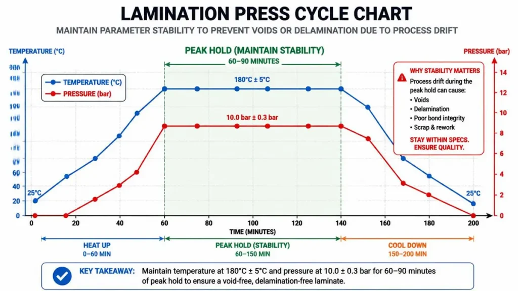
Hongda’s Precision Lamination Control Parameters to Prevent Voids and Delamination
The lamination press cycle governs the final bond quality. At Hongda, our hydraulic presses operate under closed-loop control with real-time monitoring of all critical variables:
- Temperature profile — heat is ramped to 170°C–200°C depending on dielectric resin chemistry. Precise ramp rate control (typically 2°C–5°C per minute) prevents trapped outgassing that forms voids.
- Pressure — applied in the range of 25–40 kg/cm² to ensure full wet-out of the dielectric against both the copper foil and the metal base surface topography.
- Lamination cycle time — full cure requires maintaining peak temperature for 60–90 minutes. Under-curing leaves residual stress that causes delamination under thermal cycling in the field.
- Vacuum assistance — press chambers are evacuated to below 20 mbar before pressure is applied, eliminating entrapped air and moisture that would otherwise produce void-type defects detectable only by cross-section or ultrasonic scanning.
2.4 Common Lamination Defects and Prevention
Even with mature process controls, lamination defects occur when parameters drift. The three most critical defect types are:
- Voids — air or solvent pockets within the dielectric. Prevented by adequate vacuum, correct ramp rate, and moisture-controlled material storage.
- Delamination — adhesive failure at the copper-dielectric or dielectric-metal interface. Root cause is usually surface contamination, insufficient pressure, or incompatible surface chemistry.
- Thermal conductivity non-uniformity — filler particle settling in liquid dielectrics or incomplete dielectric flow in pre-preg systems creates zones of lower thermal conductance. Prevented by material qualification testing and in-process thermal imaging of completed panels.
3. Single Layer Metal Core PCB Structure: Design, Manufacturing, and Applications
Single layer MCPCBs account for the majority of metal core PCB production volume globally. Their relative simplicity masks the manufacturing discipline required to achieve consistent performance — particularly at the dielectric layer, where layer-to-layer registration concerns are absent but adhesion quality remains paramount.
3.1 Structure Breakdown
A standard single-layer MCPCB structure, reading from top to bottom, consists of:
- Solder mask — a polymer overcoat (typically LPI liquid photo-imageable) that protects copper traces from oxidation and prevents solder bridging during assembly.
- Surface finish — OSP (Organic Solderability Preservative), ENIG (Electroless Nickel Immersion Gold), HASL, or Immersion Silver applied to exposed copper pads.
- Copper circuit layer — pattern-etched from laminated copper foil. Trace widths and clearances are designed to IPC-2221 standards.
- Dielectric layer — 75 µm to 150 µm thick in standard designs; as thin as 50 µm in high-thermal-conductivity grades.
- Metal base — 1.0 mm to 3.0 mm aluminum or copper panel providing structural rigidity and lateral heat spreading.
3.2 Typical Application Environments for Single-Layer MCPCBs
Single-layer metal core PCBs dominate in applications where high thermal load and circuit simplicity coincide:
- LED lighting arrays — high-power LED chips generate concentrated heat loads that FR4 boards cannot manage. MCPCBs extend LED lifetime from thousands to tens of thousands of hours by maintaining junction temperatures below critical thresholds.
- Motor driver modules — power MOSFETs and gate driver ICs in variable-speed drives dissipate significant switching losses that require direct thermal paths to heat sinks or chassis.
- DC-DC converter stages — synchronous rectifier and inductor assemblies benefit from the mechanical rigidity and thermal mass of aluminum-base PCBs.
- Automotive lighting and ADAS sensor boards — where both thermal performance and vibration resistance are required.
3.3 Limitations That Drive Multi-Layer Adoption
Single-layer MCPCB topology provides only one routing plane, which limits circuit complexity. Designs requiring ground planes isolated from power planes, complex signal routing, or embedded passive components must transition to multi-layer configurations. The routing constraint is the primary technical driver for multi-layer MCPCB adoption in advanced power electronics.
4. Multi-Layer MCPCB Structure: Advanced Stack-Ups for Complex Power Electronics
Multi-layer metal core PCB structures combine the thermal advantages of a metal substrate with the routing freedom of conventional multi-layer PCBs. They are inherently more complex to design and manufacture than their single-layer counterparts, demanding careful engineering of layer stack-up, copper distribution, and thermal via networks.
4.1 Multi-Layer MCPCB Stack-Up Configurations
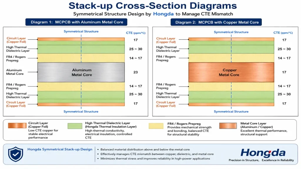
Symmetrical Multi-Layer MCPCB Stack-Up Configurations and CTE Mapping for Thermal Stress Mitigation
Two primary stack-up architectures are used in multi-layer MCPCB design:
- Metal base with conventional multi-layer sub-assembly — a separately fabricated FR4 or high-Tg multi-layer sub-stack is bonded to the metal base using a thermally conductive bonding film. Signal routing occurs in the FR4 layers; the metal base provides thermal management. This is the most producible configuration and is widely adopted at Hongda for designs requiring more than two signal layers.
- Hybrid metal-core stack-up — the metal core is embedded within the board stack-up, with FR4 or Rogers prepreg layers above and below. This configuration enables symmetrical construction and reduces warpage risk, but demands very precise CTE (Coefficient of Thermal Expansion) matching between all materials to prevent delamination under thermal cycling.
4.2 Engineering Challenges in Multi-Layer MCPCB Manufacturing
The manufacturing difficulty of multi-layer MCPCBs is substantially higher than single-layer variants:
- Layer-to-layer registration — tolerances of ±75 µm or tighter must be maintained across the full panel, requiring laser-guided pin registration systems and in-process AOI verification.
- CTE mismatch management — aluminum has a CTE of 23 ppm/°C versus 14–17 ppm/°C for FR4 and 17 ppm/°C for copper. Differential thermal expansion at interfaces generates fatigue stress on solder joints and plated vias during temperature cycling. Material selection, layer symmetry, and thermal via design all contribute to managing this stress.
- Drilling and via formation — through-hole drilling through metal-plus-FR4 composites requires carbide tooling optimized for both materials, with controlled feed rates to prevent burring at the metal-FR4 interface. Mechanical drilling remains standard; laser drilling is limited to the dielectric layers.
- Plated through-hole (PTH) reliability — electroless copper deposition must achieve uniform coverage in high-aspect-ratio holes through dissimilar materials. At Hongda, PTH pull strength is verified by IPC-TM-650 coupon testing on every production lot.
4.3 Multi-Layer MCPCB vs. Standard FR4 Multi-Layer: Performance Comparison
For designers weighing material choices, the performance delta between multi-layer MCPCB and equivalent FR4 constructions is significant:
- Thermal resistance — MCPCB constructions reduce junction-to-ambient thermal resistance by 40–70% compared to FR4 for equivalent designs, enabling higher power density or smaller board footprint.
- Mechanical stiffness — aluminum-core MCPCBs are 3–5× stiffer per unit thickness than FR4, reducing board flex and improving solder joint fatigue life in vibration environments.
- Weight — aluminum MCPCBs are lighter than equivalent copper or steel assemblies, though heavier than FR4 for the same area.
- Cost — MCPCB fabrication cost is 2–5× that of FR4 equivalents. The cost premium is justified when thermal failure, component replacement cost, or warranty liability are factored into the total ownership calculation.
5. The Complete Metal Core PCB Manufacturing Process at Shenzhen Hongda
Hongda operates an integrated manufacturing flow spanning 18 defined process stages for standard MCPCB production, with additional steps for specialty surface finishes and controlled-impedance designs. The following sequence reflects our current 2026 production process.
5.1 Stage 1 — Material Incoming Inspection and Certification
Every incoming material lot — copper foil, dielectric pre-preg, and metal base panels — is quarantined and sampled against incoming quality control (IQC) specifications before entering the production floor. Critical parameters verified include dielectric thermal conductivity (per ASTM E1461 or comparable), copper foil peel strength (per IPC-TM-650 2.4.8), and metal base dimensional tolerances. Material certificates are retained in our traceability system linked to finished board serial numbers.
5.2 Stage 2 — Metal Base Preparation
Aluminum panels are cut to production panel size (typically 18″ × 24″ or 21″ × 24″), degreased in alkaline cleaner baths, micro-etched to Ra 0.4–0.8 µm surface roughness, and inspected for flatness. Panels failing flatness criteria are rejected — not shimmed — because localized gaps in lamination pressure produce delamination-prone regions that are invisible to post-lamination electrical testing.
5.3 Stage 3 — Lamination
As detailed in Section 2, the lamination stage bonds the dielectric and copper foil to the prepared metal base under controlled temperature, pressure, and vacuum conditions. Post-lamination, panels are allowed to cool under controlled rate before pressure release to minimize residual stress. 100% of laminated panels undergo automated C-SAM (scanning acoustic microscopy) inspection for subsurface voids before advancing to the next stage.
5.4 Stages 4–8 — Imaging, Etching, and Inner Layer Processing
Circuit pattern transfer follows the standard photolithographic sequence adapted for the thermal and mechanical characteristics of MCPCB panels: dry film lamination, UV exposure through phototool, alkaline development, copper etching, and strip. Because MCPCB panels are stiffer and heavier than FR4, automated conveyorized lines are configured with modified panel support fixtures to prevent edge damage and sagging during wet processing.
5.5 Stage 9 — Drilling and Routing
CNC drilling through aluminum-composite panels requires tungsten carbide drills with optimized flute geometry and controlled chip evacuation. Feed rates are typically 30–50% lower than equivalent FR4 drilling to manage drill wear and prevent burr formation at the aluminum-dielectric interface. Panel registration is verified by X-ray coupon measurement before full production drilling commences on each lot.
5.6 Stages 10–13 — Plating, Solder Mask, and Surface Finish
Electroless and electrolytic copper plating build via and pad copper to IPC Class 2 or Class 3 thickness requirements. LPI solder mask is applied by screen or curtain coating, cured, and laser-developed. Surface finish selection — HASL, ENIG, OSP, or Immersion Silver — is application-driven, with ENIG preferred for fine-pitch BGA and SMT pads.
5.7 Stages 14–18 — Electrical Test, Inspection, Profiling, and Packaging
Flying probe electrical test verifies 100% net continuity and isolation. Automated optical inspection (AOI) checks trace geometry against Gerber data. Thermal resistance spot-check testing using IPC-configured TIM test coupons verifies that dielectric thermal conductivity has been maintained through the process. Panels are routed or punched to final board shape, inspected per IPC-A-600 Class 2/3 criteria, and packaged in nitrogen-purged vacuum bags with desiccant for moisture-sensitive surface finishes.
6. 2026 PCB Manufacturing Technology Advances Applied at Hongda
The PCB industry in 2026 is undergoing the most rapid technology transformation in a generation. Several advances directly affect MCPCB capability, cost, and sustainability — and Hongda has been actively integrating these developments into our production infrastructure.
6.1 AI-Driven Process Monitoring and Defect Prediction
Machine learning models trained on historical process data now predict lamination void probability, etch uniformity, and drill wear from inline sensor streams — enabling real-time parameter adjustment before defects occur rather than after they are detected. At Hongda, our AI monitoring system covers the lamination press, chemical etching tanks, and AOI stations, reducing scrap rates and supporting continuous process improvement cycles that would be impossible with human-only review.
6.2 High-Thermal-Conductivity Dielectric Materials
The availability of commercial dielectric systems achieving 6–10 W/m·K thermal conductivity — versus the 1–3 W/m·K typical of prior-generation materials — has fundamentally expanded MCPCB application scope. These advanced materials use ceramic fillers (Al₂O₃, AlN, BN) in polymer matrices that maintain processability on standard lamination equipment. Hongda has qualified three ceramic-composite dielectric systems in 2025–2026 to serve customers in EV power electronics, industrial laser drivers, and RF power amplifiers.
6.3 Additive and Semi-Additive Circuit Formation
Traditional subtractive etching removes copper to define circuit features, generating significant chemical waste. Modified Semi-Additive Process (mSAP) and fully additive printing techniques, increasingly available in 2026 for MCPCB applications, build copper conductors selectively on the substrate — reducing copper consumption by up to 50% and enabling finer line widths (25 µm and below) that are difficult to achieve by subtractive etching on thermally conductive substrates. Hongda is piloting mSAP capability for fine-pitch power module applications.
6.4 Industry 4.0 Traceability and Connected Manufacturing
End-to-end digital traceability — from material lot through shipping — is no longer optional for customers in automotive, medical, and aerospace supply chains. Hongda’s 2026-implemented MES (Manufacturing Execution System) records every process parameter, operator action, and machine calibration event against each panel’s unique barcode. This data trail enables root-cause analysis of field returns with precision previously unattainable and supports customers’ own PPAP and first-article documentation requirements.
6.5 Sustainable Manufacturing Practices
Environmental compliance pressure — IPC-1752A, EU RoHS, REACH, and emerging carbon reporting requirements — is accelerating the adoption of halogen-free dielectric materials, closed-loop copper etch chemistry recycling, and reduced-VOC solder mask systems across the MCPCB supply chain. Hongda’s environmental management system is certified to ISO 14001:2015, and our 2025–2026 capital investment program has included a copper recovery system that reclaims over 95% of copper from etchant solutions for off-site refining.
7. How to Specify a Metal Core PCB: Key Parameters for Engineers and Buyers
Specifying an MCPCB for a new design requires defining parameters that FR4 engineers may not be accustomed to. The following checklist covers the critical variables to communicate to your manufacturer:
- Metal base material and thickness — aluminum 1.0 mm, 1.5 mm, 2.0 mm, or 3.0 mm; copper 1.0 mm or 2.0 mm; specify alloy grade if critical.
- Dielectric thermal conductivity — state the minimum acceptable value in W/m·K. If thermal resistance budget is known, state the maximum acceptable Rth in °C·cm²/W.
- Dielectric thickness — specify in µm; thinner dielectric lowers thermal resistance but may reduce dielectric breakdown voltage.
- Copper weight — specify in oz/ft² for circuit layer; 1 oz (35 µm) is standard, 2 oz (70 µm) or 3 oz (105 µm) for high-current traces.
- Number of layers — single, double-sided (with through-hole interconnect), or multi-layer sub-stack configuration.
- Surface finish — HASL, ENIG, OSP, ImAg, or ImSn; specify RoHS compliance if required.
- IPC class — Class 2 for commercial/industrial, Class 3 for high-reliability/automotive/military.
- Controlled impedance — if required, specify target impedance values and tolerance (±10% or tighter).
8. Why Partner with Shenzhen Hongda Circuit Technology for MCPCB Manufacturing
Choosing an MCPCB manufacturer is not simply a transaction — it is a selection of a process engineering partner whose capability and quality discipline directly determine whether your product meets its thermal, reliability, and cost targets in the field.
Shenzhen Hongda Circuit Technology Co., Ltd. brings together deep process expertise in metal core PCB lamination, materials engineering, and precision fabrication, supported by an ISO 9001:2015 certified quality management system and the 2026 technology capabilities described in this article. Our engineering team provides design-for-manufacturability (DFM) review for every new design, identifying stack-up risks, via design issues, and material selection improvements before tooling is cut.
We support production volumes from engineering prototype quantities (as few as 5 panels) through high-volume series builds, with consistent process parameters across all quantities. Customers receive full traceability documentation, third-party test reports on request, and technical application support throughout the product lifecycle.
Whether your application is LED system design, EV power electronics, industrial motor control, or defense-grade thermal management, Hongda’s metal core PCB manufacturing capabilities are engineered to meet your most demanding specifications.
Conclusion: Lamination Precision and Structural Engineering Define MCPCB Performance
The performance of any metal core PCB — its thermal conductance, electrical integrity, mechanical stability, and long-term reliability — is determined less by the selection of materials alone than by the precision and discipline with which those materials are processed. The metal core PCB manufacturing process is a cascade of interdependent stages where each step either builds on the quality established by the previous one or compounds its deficiencies.
In 2026, the MCPCB industry stands at a point where advances in high-thermal-conductivity dielectrics, AI-augmented process control, additive circuit formation, and end-to-end digital traceability are simultaneously raising the performance ceiling and lowering the defect floor for manufacturers that invest in these capabilities. Shenzhen Hongda Circuit Technology is committed to maintaining its position at this frontier — delivering metal core PCBs that give our customers the thermal margins, reliability headroom, and manufacturing repeatability their products demand.
To request a technical consultation, design review, or quote for your MCPCB application, contact Shenzhen Hongda Circuit Technology Co., Ltd. through our official channels.
FAQs
1How do I choose a reliable Metal Core PCB manufacturer in China?
When evaluating a metal core PCB manufacturer, procurement teams should verify four core qualifications before requesting a quote:
Certifications — ISO 9001:2015 quality management and ISO 14001:2015 environmental compliance are minimum requirements. IPC membership and UL recognition indicate adherence to international PCB standards.
Process capability — confirm the manufacturer operates dedicated MCPCB lamination lines with vacuum-assisted presses and in-line C-SAM inspection. Shared FR4/MCPCB lines compromise process control.
Thermal performance verification — request third-party thermal resistance test data (per IPC-TM-650) on the specific dielectric material proposed for your design, not generic datasheet values.
Traceability — for automotive and industrial supply chains, full material-lot-to-board traceability supported by an MES system is required. Verify this before committing to a supplier.
What is the typical lead time for Metal Core PCB manufacturing and what affects it?
Standard metal core PCB lead time depends on design complexity, layer count, surface finish, and order quantity. Typical ranges:
Engineering prototypes (5–20 panels) — 5 to 7 business days for single-layer aluminum MCPCBs with HASL or OSP finish.
Small-series production (up to 500 panels) — 10 to 15 business days, including dielectric qualification and electrical test.
Volume production (500+ panels) — 15 to 25 business days depending on copper weight, surface finish (ENIG adds 1–2 days), and controlled-impedance testing requirements.
Key factors that extend lead time: ENIG or Immersion Silver finishes, multi-layer MCPCB configurations, high-thermal-conductivity dielectric materials requiring special procurement, and orders requiring third-party test reports. Always communicate these requirements upfront to avoid schedule surprises.
What thermal conductivity values are available for Metal Core PCB dielectric layers?
The thermal conductivity of MCPCB dielectric is one of the most critical specifications buyers must define. Available grades in 2026:
Economy grade (1.0–2.0 W/m·K) — standard polymer-filled systems. Suitable for LED lighting arrays and low-power motor drivers where cost is the primary constraint.
Mid-range grade (2.0–4.0 W/m·K) — ceramic-filled polymer systems (Al₂O₃ filler). Recommended for industrial power supplies and EV auxiliary electronics.
High-performance grade (4.0–6.0 W/m·K) — high-loading ceramic composite systems. Used in high-power inverters, traction motor drives, and telecom base-station power modules.
Premium grade (6.0–10.0+ W/m·K) — AlN or BN ceramic matrix systems. Specified for defense electronics, industrial laser drivers, and high-density RF power amplifiers.
What certifications and quality standards should a PCB supplier hold for automotive or industrial use?
For automotive PCB suppliers and industrial-grade procurement, the certification baseline is significantly higher than for commercial electronics. Buyers should require:
ISO 9001:2015 — mandatory quality management foundation for any serious PCB supplier.
IATF 16949 — the automotive sector supplement to ISO 9001. Required for direct automotive OEM supply chains. Confirms the supplier operates APQP, FMEA, and PPAP processes.
IPC-A-600 Class 3 — highest acceptability class for PCB workmanship. Required for high-reliability applications including automotive safety systems and medical electronics.
RoHS and REACH compliance — legally mandatory for EU market access. Confirm material certificates cover the specific dielectric and surface finish in your design.
UL recognition — required for products requiring UL listing in North American markets. Verify the specific board material combination is covered by the UL file.
What information do I need to provide to get an accurate Metal Core PCB quote?
An accurate MCPCB quote requires more information than a standard FR4 PCB request. Provide the following upfront to avoid revision cycles:
Gerber files + drill files — RS-274X format with board outline in the mechanical layer.
Layer stack-up specification — layer count, copper weight (oz/ft²), dielectric thickness (µm), metal base thickness (mm).
Thermal conductivity requirement — minimum W/m·K, or thermal resistance budget in °C·cm²/W.
Metal base material — aluminum alloy (5052 or 6061) or copper. State alloy grade if critical.
Surface finish — HASL (lead-free), ENIG, OSP, Immersion Silver, or Immersion Tin. State RoHS requirement.
IPC class — Class 2 (commercial/industrial) or Class 3 (high-reliability). Affects inspection criteria and pricing.
Quantity and delivery schedule — prototype vs. production volume, and required ship date.
Special requirements — controlled impedance, thermal resistance coupon testing, third-party inspection, or specific packaging.
About Author
David Chen https://www.linkedin.com/in/pcbcoming
David Chen boasts an extensive professional background in PCBA manufacturing, PCBA testing, and PCBA optimization, with specialized expertise in high-precision PCBA fault analysis and rigorous PCBA reliability testing. The author has worked with high-layer-count server PCB fabrication, ultra-low-loss backplane stackups, and thermo-mechanical reliability optimization for AI infrastructure projects involving 112G and 224G PAM4 architectures. Skilled in complex circuit design and cutting-edge advanced PCB manufacturing processes, he delivers solutions that elevate product durability and performance across industrial applications. His technical articles focusing on PCBA manufacturing workflows and testing methodologies are widely cited by industry peers, research institutions, and technical platforms, solidifying his reputation as a recognized technical authority in the global circuit board manufacturing sector.