Impedance Control, ENIG Surface Finish & High-Speed Circuit Solutions
Introduction: Why PCB Manufacturing Technology Defines the Future of Electronics in 2026
The global printed circuit board (PCB) industry is undergoing one of its most transformative periods in history. As artificial intelligence accelerates hardware demands — from AI inference servers and GPU accelerator cards to 5G base stations and autonomous vehicle systems — the tolerance for signal integrity failure has dropped to near zero. In 2026, the gap between a mediocre PCB supplier and a precision circuit board manufacturer is measured not just in microns, but in competitive advantage.
At Shenzhen Hongda Circuit Technology Co., Ltd., we have built our manufacturing capability around two pillars that define reliable high-speed PCB performance: tight impedance control and ENIG (Electroless Nickel Immersion Gold) surface treatment. This article provides a comprehensive, data-driven look at how these technologies work, how they interact, and why procurement teams worldwide should understand them before selecting a PCB manufacturing partner.
Section 1: The 2026 PCB Manufacturing Landscape — High-Speed Demands Are Reshaping the Industry
1.1 Signal Integrity Requirements for AI and High-Speed Digital PCB Design
Modern AI server boards, HPC (high-performance computing) substrates, and SerDes-based communication boards routinely operate at data rates exceeding 25 Gbps per lane — and increasingly at 56 Gbps or 112 Gbps with PAM4 signaling. At these speeds, any deviation in trace geometry, dielectric consistency, or surface conductivity directly translates into signal degradation, eye diagram closure, or bit error rate (BER) failures.
The PCB manufacturing process in 2026 must therefore support:
- Differential impedance control within ±5% tolerance across the full panel
- Ultra-low-loss laminate materials with stable Dk/Df across temperature and frequency
- Flat, solderable, and signal-transparent surface finishes that do not distort impedance at high frequencies
- Layer stack-up engineering validated by electromagnetic field simulation tools
1.2 How PCB Technology Specifications Have Evolved for AI Hardware
The rise of AI accelerators (such as next-generation GPU clusters and NPU boards) has pushed PCB layer counts to 20–40 layers, with trace widths as narrow as 3 mil and dielectric thicknesses under 3 mil for critical impedance layers. These boards demand a manufacturing partner capable of holding these parameters consistently — not on prototype runs, but at volume production scale.
Shenzhen Hongda Circuit Technology has invested in precision etching lines, real-time AOI inspection, and TDR (Time Domain Reflectometry) testing infrastructure to meet these exacting standards. Our 2026 manufacturing data shows consistent Cpk values above 1.33 on controlled impedance layers, reflecting a process capability that exceeds typical industry standards.
Section 2: PCB Impedance Control — Manufacturing Methods, Materials & Measurement
2.1 What Is Impedance Control in PCB Manufacturing?
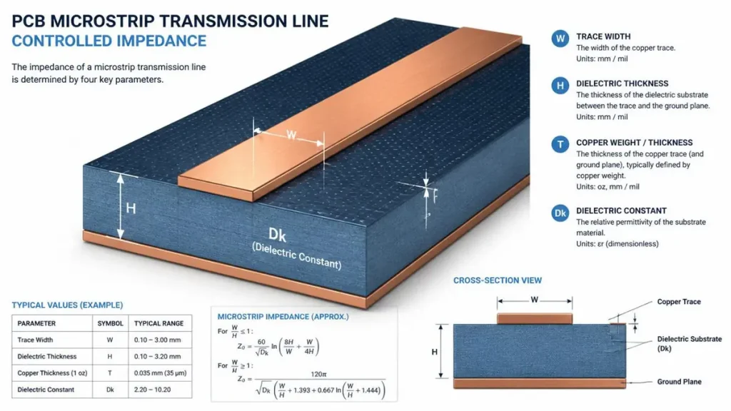
PCB Microstrip Transmission Line – Impedance Control Parameters
Controlled impedance in PCB manufacturing refers to the engineering discipline of ensuring that transmission lines on a circuit board maintain a specified characteristic impedance — most commonly 50Ω for single-ended traces and 85Ω or 100Ω for differential pairs. When an electrical signal travels along a trace whose impedance does not match the expected value, reflections and discontinuities occur, degrading signal quality.
For a PCB manufacturer, achieving controlled impedance means simultaneously managing four interdependent physical parameters:
- Trace width and spacing (linewidth accuracy after chemical etching)
- Dielectric thickness (Prepreg / Core layer height consistency)
- Copper foil weight (trace thickness uniformity)
- Dielectric constant (Dk) of the laminate material
2.2 High-Performance Laminate Materials for Precision PCB Impedance
Material selection is foundational to impedance control. Standard FR-4 laminates, while adequate for consumer electronics, exhibit dielectric constant variation with frequency and temperature that becomes problematic above 5 GHz. In 2026, high-speed PCB designs demand materials such as:
- Panasonic Megtron 6/7 — Dk of approximately 3.6 at 10 GHz with very low Df (~0.004), ideal for 56G/112G SerDes applications
- Isola IT-180A — stable Dk/Df through thermal cycling, commonly specified for industrial and server-grade boards
- Rogers 4350B — widely used in RF and microwave PCB applications requiring consistent Dk across wide frequency ranges
Shenzhen Hongda maintains an approved material library and works directly with leading laminate manufacturers to source controlled-lot materials that carry traceable Dk/Df characterization data — a critical factor when the PCB procurement process involves engineering validation.
2.3 Etching Compensation and Process Control in High-Precision PCB Fabrication
One of the most technically demanding aspects of impedance-controlled PCB manufacturing is etching compensation. Because chemical etching is an isotropic process (it removes copper in all directions simultaneously), the final trace width on the board is narrower than the design artwork width. The amount of this “etch factor” varies based on copper weight, etchant chemistry, temperature, and dwell time.
Experienced PCB manufacturers model the etch factor based on historical process data and pre-compensate the photoplot artwork before imaging. At Shenzhen Hongda:
- Etch compensation is applied per copper weight and layer type
- Inner-layer core processing is separated from outer-layer processing to isolate variables
- Real-time SPC (Statistical Process Control) monitors etch line parameters to detect drift before panels are produced
2.4 TDR Testing and Impedance Coupon Design — The Verification Standard
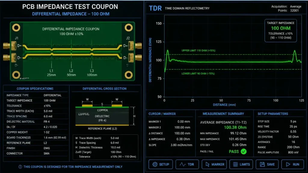
PCB Impedance Test Coupon and TDR Testing Waveform
Impedance verification in production PCB manufacturing uses TDR (Time Domain Reflectometry) — a technique that injects a fast-rise-time pulse into a transmission line and measures the reflected voltage waveform. Deviations from the expected impedance appear as reflections, enabling precise measurement of the actual trace impedance.
Industry best practice and most OEM customer specifications require that impedance test coupons be placed on each panel, in a location representative of the actual production traces. Our standard coupon design includes:
- 50Ω single-ended microstrip and stripline reference structures
- 100Ω and 85Ω differential pair structures
- Length-matched coupons for accurate TDR measurement repeatability
Every production panel at Shenzhen Hongda is 100% TDR tested before shipment. Test results — including measured vs. target impedance and Cpk statistics — are archived and provided to customers in a formal impedance test report as part of the delivery documentation package.
Section 3: PCB Surface Finish Technology — ENIG vs. LF HASL for High-Speed Applications
3.1 How Surface Finish Affects Signal Integrity and PCB Performance
A PCB surface finish is not merely a solderability protection layer — at high frequencies, it becomes an active part of the signal transmission path. At frequencies above 1 GHz, the skin effect causes RF current to concentrate on the outermost micrometers of a conductor surface. The roughness and conductivity of the surface finish directly influence insertion loss on high-speed differential pairs.
Two surface finish characteristics are most critical from a signal integrity standpoint:
- Surface roughness — rougher surfaces increase the effective path length for high-frequency current, raising conductor loss
- Coating uniformity — non-uniform coating introduces local impedance discontinuities that cause reflections and degrade eye opening
3.2 LF HASL (Lead-Free Hot Air Solder Leveling) — Capabilities and Limitations
LF HASL (Lead-Free Hot Air Solder Leveling) is a mature, cost-effective surface finish widely used in consumer electronics. In this process, the PCB is dipped in a molten solder bath and hot air knives remove the excess, leaving a solder-coated copper surface.
While LF HASL is suitable for many standard applications, it presents challenges for high-speed designs:
- Uneven surface topography — HASL surfaces vary in height by 10–30 µm across a pad, making coplanarity difficult for BGA and fine-pitch components
- Non-uniform conductor thickness — the variable solder thickness changes the local effective trace geometry, shifting impedance away from design targets
- Limited fine-pitch compatibility — below 0.4 mm pitch BGAs or 0.3 mm QFP, HASL bridging risk increases
- Higher surface roughness — the solder grain structure introduces roughness that increases conductor loss at frequencies above 5 GHz
3.3 ENIG Surface Finish — Technical Advantages for High-Speed PCB Manufacturing in 2026
ENIG (Electroless Nickel Immersion Gold) is the surface finish of choice for precision high-speed PCBs. In this two-step chemical deposition process, a controlled layer of nickel (typically 3–6 µm) is deposited on the copper, followed by a thin immersion gold layer (typically 0.05–0.12 µm) that protects the nickel from oxidation.
The technical advantages of ENIG over LF HASL for high-speed digital PCBs are substantial:
- Exceptional surface planarity — ENIG deposits uniformly at the molecular level, producing pad-to-pad height variation below 2 µm, critical for fine-pitch BGA assembly yields
- Controlled coating thickness — the electroless chemistry self-limits, producing consistent Ni/Au thickness regardless of pad geometry
- Lower surface roughness — the ENIG surface exhibits significantly lower roughness than HASL, reducing conductor loss at frequencies above 10 GHz
- More stable impedance environment — the uniform, consistent surface geometry of ENIG minimizes the impedance variation that rough or uneven finishes introduce
- Better compatibility with HDI structures — ENIG is compatible with via-in-pad designs and stacked microvia structures common in HDI and any-layer PCBs
3.4 Why AI Server and High-Speed Backplane PCBs Require ENIG — Data-Driven Analysis
For PCB designs operating above 10 GHz or carrying data lanes at 25 Gbps and beyond, the choice of surface finish is not a cost optimization decision — it is a signal integrity engineering decision. Comparative measurements on identical board designs with LF HASL vs. ENIG surface finish consistently show:
- 3–6 dB reduction in insertion loss at 10 GHz for ENIG vs. LF HASL on 100Ω differential pairs
- Improved eye diagram opening — ENIG boards show measurably wider eye height and width at 25 Gbps NRZ signaling
- Reduced impedance deviation — ENIG boards show tighter actual-vs-design impedance distribution (σ 1.2Ω vs. 2.8Ω in representative TDR data)
These performance differences are why leading hyperscale data center operators, AI accelerator card ODMs, and high-speed networking equipment manufacturers specify ENIG as the mandatory surface finish for all controlled-impedance PCBs.
Section 4: Shenzhen Hongda Circuit Technology — 2026 PCB Manufacturing Capabilities Overview
4.1 Core PCB Manufacturing Specifications
Shenzhen Hongda Circuit Technology Co., Ltd. is a professional PCB manufacturer based in Shenzhen, China, specializing in high-reliability, high-speed, and impedance-controlled circuit boards. Our 2026 manufacturing capability profile includes:
- Layer count: 2 to 40 layers
- Minimum trace width/space: 3 mil / 3 mil
- Controlled impedance tolerance: ±5% standard; ±3% available on request
- Surface finish options: ENIG, LF HASL, ENEPIG, OSP, Immersion Silver, Immersion Tin
- Laminate materials: Standard FR-4, High-Tg FR-4, Megtron 6/7, IT-180A, Rogers series
- Maximum panel size: 21″ × 24″
- PCB thickness range: 0.4 mm to 6.0 mm
- Via types: Through-hole, blind, buried, microvia (laser-drilled)
- Copper weight: 0.5 oz to 6 oz outer layer; 0.5 oz to 3 oz inner layer
4.2 Quality Assurance and Certification
Quality at Shenzhen Hongda is embedded at the process level, not inspected at the end. Our quality management infrastructure includes:
- ISO 9001:2015 certified quality management system
- IPC-A-600 Class 2 and Class 3 acceptance criteria
- 100% electrical test (flying probe or fixturized bed-of-nails)
- 100% AOI (Automated Optical Inspection) on inner and outer layers
- TDR impedance testing on every controlled-impedance panel
- ITAR-compliant handling procedures available for defense and aerospace customers
4.3 Stack-Up Engineering and DFM Support
One of the most common sources of impedance deviation in PCB manufacturing is inadequate stack-up planning. Shenzhen Hongda provides complimentary Design for Manufacturability (DFM) review and stack-up engineering support for all qualified projects. Our engineering team analyzes:
- Dielectric material selection and actual Dk/Df characterization at operating frequency
- Layer assignment for controlled impedance traces (microstrip vs. stripline recommendation)
- Via stub mitigation (back-drilling capability available)
- Impedance trace width pre-calculation validated by our in-house simulation tool
This collaborative engineering approach ensures that the PCB design arriving at manufacturing is optimized for our specific process — reducing first-article iteration cycles and compressing time-to-volume production.
FAQ for PCB Procurement Professionals
How do I evaluate a PCB manufacturer’s impedance control capability before placing an order?
The most reliable indicator of a PCB manufacturer’s impedance control capability is the combination of their process Cpk data and their TDR testing infrastructure. Ask the supplier to provide: (1) their standard impedance tolerance specification (±5% is the IPC-2141 baseline; ±3% indicates a more capable process); (2) sample TDR test reports showing measured vs. designed impedance for recent production panels; and (3) their Cpk values for a 50Ω and 100Ω reference. A Cpk above 1.33 indicates a capable process with fewer than 64 defects per million opportunities. Additionally, verify that impedance coupons are included on every production panel — not just prototype runs — and that the supplier maintains traceable material certification records for the laminate Dk values used in impedance calculations.
What is the difference between ENIG and HASL surface finish, and which should I specify for my high-speed PCB?
ENIG (Electroless Nickel Immersion Gold) and LF HASL (Lead-Free Hot Air Solder Leveling) differ fundamentally in how the finish is deposited. HASL applies solder by hot-dipping and leveling with high-pressure air knives, which produces an uneven surface with height variation of 10–30 µm. ENIG deposits nickel and gold through controlled chemical reactions, producing an extremely flat, uniform surface with sub-2 µm variation. For high-speed PCBs — any design with differential pairs, BGA components, or data rates above 5 Gbps — ENIG is strongly preferred. The flat ENIG surface maintains consistent trace geometry and copper-to-dielectric-to-finish relationships, which directly supports stable, repeatable impedance. HASL’s surface variability introduces impedance discontinuities and increased conductor loss that become significant above 5 GHz. For cost-sensitive, lower-frequency boards, LF HASL remains a practical choice.
What PCB certifications and quality standards should I require from a Chinese PCB manufacturer?
A credible Chinese PCB manufacturer for OEM/ODM supply should hold at minimum: ISO 9001:2015 (quality management system); UL certification for the PCB product itself (check the UL file number against the UL database); and IPC membership with adherence to IPC-A-600 acceptance criteria at Class 2 or Class 3 level. For regulated industries, additional certifications matter: ISO 13485 for medical devices, AS9100 for aerospace, or IATF 16949 for automotive. Beyond certificates, request evidence of their quality system in action: recent internal audit reports, customer 8D reports showing corrective action history, and outgoing quality rate (OQR) data. Shenzhen Hongda Circuit Technology maintains all primary certifications and provides customers with full material traceability documentation and production traveler records for each order.
How do I specify HDI PCBs with blind and buried vias to a manufacturing supplier, and what lead times should I expect in 2026?
When specifying HDI (High Density Interconnect) PCBs with blind and/or buried vias, the most important document is your cross-section (stack-up) drawing with via definitions clearly called out by span — for example, ‘L1-L2 blind via, laser-drilled, 0.1 mm diameter’ and ‘L3-L6 buried via, 0.2 mm drill.’ Provide a complete Gerber package (IPC-2581 format is increasingly preferred), a drill file that separates via types, controlled impedance requirements, and your laminate material preference. HDI PCBs typically require more build cycles and have longer lead times than standard through-hole boards. In 2026, standard lead times for prototype HDI PCBs (any-layer or 1-2-1 build) run 7–15 working days; mass production lead times are typically 18–25 working days depending on layer count and surface finish. Expedite programs are available from qualified suppliers.
What are the key technical questions to ask when sourcing PCBs for AI server or data center hardware from a contract manufacturer?
When qualifying a PCB contract manufacturer for AI server or data center hardware, the technical questions that separate capable suppliers from marginal ones include: (1) What is your maximum supported signal layer count and what impedance tolerance can you hold at volume? (2) What low-loss laminate materials do you have approved in your material qualification library, and do you have Dk/Df test data at 10 GHz and above? (3) Can you support back-drilling (controlled-depth drilling) to remove via stubs that cause resonance on high-speed lanes? (4) What is your inner-layer registration accuracy, and how do you validate it for 20+ layer designs? (5) Do you provide TDR test reports and impedance coupon data as standard deliverables, or only on request? Suppliers unable to answer these questions with specific data and process documentation are unlikely to meet the quality bar for AI hardware applications, where board-level failures can cascade into system downtime and significant commercial impact.
Choosing the Right PCB Manufacturing Partner in 2026
The electronics hardware landscape of 2026 demands more from PCB manufacturing technology than at any previous point in the industry’s history. High-speed AI infrastructure, data center networking equipment, and next-generation communication systems all depend on circuit boards that deliver precise impedance control, low insertion loss, and consistent surface finish quality at volume production scale.
Shenzhen Hongda Circuit Technology Co., Ltd. has built its manufacturing capability around exactly these requirements. Through mastery of impedance-controlled PCB fabrication, ENIG surface finish processing, advanced laminate material management, and TDR-verified quality assurance, we deliver the signal integrity performance that modern electronics designs demand.
We invite procurement teams, hardware engineers, and supply chain professionals to engage with our engineering team for DFM review, stack-up consultation, and sample evaluation. The precision your design demands starts with the manufacturing partner you choose.
Shenzhen Hongda Circuit Technology Co., Ltd.
Precision PCB Manufacturing | Impedance Control | ENIG Surface Finish | High-Speed PCB Solutions
About Author
David Chen https://www.linkedin.com/in/pcbcoming
David Chen boasts an extensive professional background in PCBA manufacturing, PCBA testing, and PCBA optimization, with specialized expertise in high-precision PCBA fault analysis and rigorous PCBA reliability testing. The author has worked with high-layer-count server PCB fabrication, ultra-low-loss backplane stackups, and thermo-mechanical reliability optimization for AI infrastructure projects involving 112G and 224G PAM4 architectures. Skilled in complex circuit design and cutting-edge advanced PCB manufacturing processes, he delivers solutions that elevate product durability and performance across industrial applications. His technical articles focusing on PCBA manufacturing workflows and testing methodologies are widely cited by industry peers, research institutions, and technical platforms, solidifying his reputation as a recognized technical authority in the global circuit board manufacturing sector.