Heavy Copper PCB Design Guidelines: Trace Width, Clearance, and DFM Essentials
Document Introduction: This is the full 2026 technical specification for heavy copper PCB, covering EV inverters, solar converters, motor drives, welding equipment and other high-power electronics. It contains etch back compensation rules, trace & clearance standards, DFM checklist, new manufacturing processes and supplier selection guidance.
Heavy copper PCB technology is no longer a niche request from power electronics teams — it has become the default board build for EV traction inverters, solar and wind power converters, motor drives, battery management systems, and industrial welding equipment. More copper cross-section lowers resistance, lowers I²R heating, and lets a board carry current that a standard 1oz layout simply cannot handle in the same footprint.
What trips up engineering teams isn’t the concept. It’s etch back — the copper undercut produced when thick copper foil is etched — quietly narrowing every trace and closing up every clearance gap on the finished board, even when the Gerber file looks correct. At Shenzhen Hongda Circuit Technology Co., Ltd., our engineering team reviews incoming heavy copper PCB designs every week, and etch back compensation is still the number-one reason a first article comes back under-rated or fails clearance verification.
This guide covers how heavy copper etches differently from standard copper, how to set trace width and clearance with the right compensation built in from the start, what a proper heavy copper PCB DFM review should check before a board goes to fabrication, and the manufacturing technology shift that’s changed how heavy copper PCB manufacturers in China are running these processes in 2026.
What Is a Heavy Copper PCB? Definition, Etch Back, and Design Challenges
Heavy Copper PCB Definition: 3oz, 4oz, and 8oz Copper Thickness
Copper weight on a PCB is measured in ounces per square foot. Standard boards run 1oz (about 35µm) or 2oz (about 70µm) finished copper. A board earns the label heavy copper PCB once finished copper reaches 3oz (roughly 105µm) and up — 4oz, 6oz, 8oz, and in extreme-current designs 10oz or more. That 3oz line isn’t a marketing threshold; it’s the point where etching, plating, and lamination all start behaving differently enough that 1oz-era design rules stop applying.
Heavy Copper PCB Manufacturing vs. Standard PCB Manufacturing
Thicker copper takes longer to clear in the etch bath, and etch time is exactly where the risk builds. A 1oz layer clears an open field in a short cycle with almost no sidewall loss. A 4oz or 8oz layer needs several times that dwell time to remove the same field copper, and every extra minute in the bath eats into trace sidewalls as well as open copper. Plating current density also spreads unevenly across a large panel, so on a heavy copper PCB, thickness uniformity has to be actively controlled rather than assumed — which is part of why heavy copper PCB manufacturer selection matters more than it does for a standard 2-layer board.
Etch Back in Heavy Copper PCB Fabrication, Explained
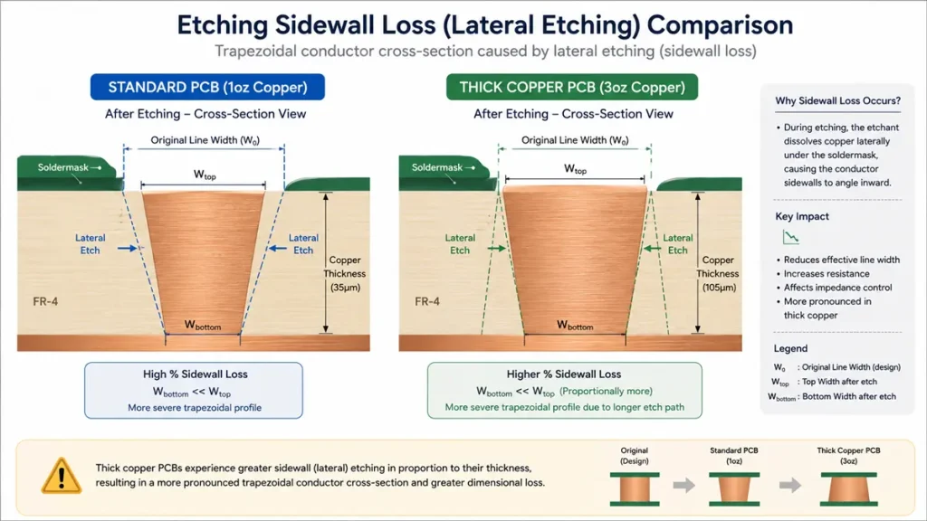
Cross-Sectional Comparison of Etch Back and Sidewall Loss Between 1oz Standard PCB and 3oz Heavy Copper PCB
Etching isn’t perfectly vertical. As etchant works down through copper thickness, it also attacks the trace sidewalls from both edges. On 1oz copper that lateral bite is small enough to ignore. On heavy copper it isn’t — sidewall contact time is much longer, so the finished trace ends up trapezoidal in cross-section: narrower at the base than at the top, and thinner overall than what the design file specified.
How Etch Back Changes Trace Width, Clearance, and Current Rating
Uncompensated etch back creates three problems that only appear once the board is built:
- Trace width shrinks below the drawn value, cutting directly into current-carrying capacity.
- Clearance closes up as neighboring copper loses width on both sides, raising short-circuit and arcing risk.
- Current rating drifts away from the original IPC-2152 calculation, because actual copper cross-section is smaller than the design assumed.
None of this shows up in CAM review. It shows up on the bench, during bring-up, which is exactly why compensation belongs at the layout stage — not as a fix applied after a failed prototype.
Etch Back Compensation for Heavy Copper PCB: Design Fundamentals
Anisotropic Etching and Copper Undercut on Heavy Copper PCB
Etching removes copper at different rates vertically and laterally — that mismatch is what “anisotropic” means in this context, and it grows worse as copper gets thicker. As a working planning figure, many heavy copper PCB fabricators budget roughly 0.5–1 mil of sidewall undercut per ounce of copper, per side. On an 8oz layer, that adds up to several mils of lost width before any other process tolerance is even factored in.
Why Etch Back Compensation Design Is Non-Negotiable Above 3oz Copper
Under 2oz, most designers can skip explicit compensation because the loss falls inside normal manufacturing tolerance anyway. Above 3oz, that assumption breaks. Skip compensation on a heavy copper PCB design and you’re almost guaranteed a gap between the current rating you calculated and the current rating of the physical board — a gap that surfaces during bring-up, or worse, after the product ships.
Copper Weight, Target Width, and Fab Capability: Three Compensation Variables
Three inputs set the compensation factor:
- Copper weight — heavier copper needs a larger width allowance.
- Target finished trace width — narrower targets are proportionally more sensitive to the same absolute undercut.
- Fabricator process capability — etch chemistry, line control, and equipment differ between manufacturers, so the same nominal copper weight can produce different real-world undercut depending on who’s running the panel.
That third variable is where most design teams go wrong. Etch back compensation is not a constant pulled from a generic datasheet — it’s a process capability figure, and it should come from the fabricator actually building the board, not from a rule of thumb copied from an old project.
Heavy Copper PCB Trace Width Design Guidelines (3oz / 4oz / 8oz Copper PCB)
3oz Copper PCB Trace Width Design Recommendations
For 3oz copper PCB designs, most production lines can reliably hold a finished minimum trace width around 8–10 mil, provided the design file carries enough compensation to offset etch back. Dropping below that band sharply raises the risk of open circuits where over-etching occurs on isolated, fine-pitch trace runs.
4oz Copper PCB Trace Width Design Recommendations
4oz copper PCB layouts generally push the practical minimum finished trace width to around 10–12 mil. At this thickness, a lone thin trace surrounded by wide copper pours is especially vulnerable — the etchant clears open field copper faster than it clears around an isolated feature, so uneven exposure can push undercut beyond the average figure used for planning.
8oz Copper PCB Trace Width Design Recommendations
8oz and heavier copper PCB builds typically need a finished minimum trace width in the 15–20 mil range. Above 6oz, we recommend a direct DFM conversation with your fabricator before the layout is locked, since process capability varies more at this thickness than at any other copper weight.
Trace Width Compensation: Design Value vs. Finished Value on Heavy Copper PCB
The working method is straightforward: settle on the finished trace width your current-carrying calculation requires, then add the fabricator’s quoted etch compensation to get the design value you actually draw. On a 4oz board needing a 12 mil finished trace, with a 3 mil compensation factor for that copper weight, the design file should call out 15 mil. Skipping this arithmetic is the single most common reason heavy copper PCB prototypes come back under-rated for current.
Building Redundancy Into High-Current Trace Width
Etch back, plating tolerance, and thermal derating all stack against a heavy copper design at once, so it’s worth sizing trace width with headroom rather than to the exact IPC-2152 minimum. A trace carrying 15–20% margin above the calculated minimum absorbs normal process variation without pushing temperature rise close to failure territory.
Heavy Copper PCB Clearance Design Rules and Minimum Spacing Guidelines
Why Clearance Design Prevents Short Circuits on Heavy Copper PCB
Clearance is the physical margin that keeps adjacent copper from arcing, bridging, or shorting under voltage and thermal stress — not a formality on a drawing. Heavy copper boards typically run higher current and, in many applications, higher voltage as well, which makes clearance design more consequential than it is on a standard-weight board.
Minimum Clearance by Copper Weight: 3oz vs. 4oz vs. 8oz Copper PCB
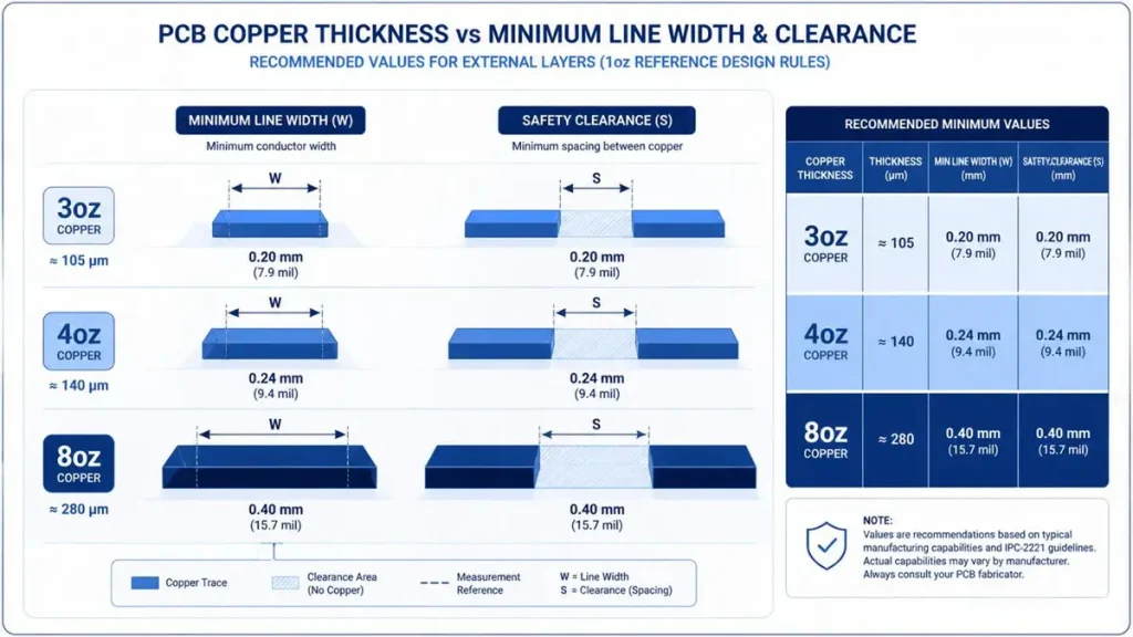
Dimensional Guide – Recommended Minimum Line Width (W) and Safety Clearance (S) for 3oz, 4oz, and 8oz Heavy Copper External Layers.
| Copper Weight | Minimum Trace Width | Minimum Clearance |
|---|---|---|
| 3oz | 8–10 mil | 8–10 mil |
| 4oz | 10–12 mil | 10–12 mil |
| 8oz | 15–20 mil | 15–20 mil |
These clearance figures track the trace width figures closely because both are driven by the same etch back mechanism.
How Etch Back Amplifies Clearance Loss on Heavy Copper PCB
Etch back cuts copper from both sides of a gap at once. Every mil of undercut recovered on one feature’s edge widens the gap on that side — but the extra width an engineer adds to compensate a trace narrows the clearance sitting right next to it. Trace width compensation and clearance can’t be solved independently on a heavy copper PCB; a fix for one can quietly break the other if they’re not reviewed together.
High-Voltage Heavy Copper PCB Clearance Requirements (IPC-2221)
Where a heavy copper board also runs elevated voltage, IPC-2221 electrical clearance requirements for that operating voltage need to be checked against the heavy-copper-adjusted minimum, and the larger of the two figures governs. High-voltage heavy copper PCB designs — common in EV traction inverters and industrial drive electronics — frequently need clearance well beyond the baseline heavy copper minimum shown above.
Common Heavy Copper PCB Design Mistake: Standard 1oz Clearance Rules
The most frequent DFM failure our engineering team flags on incoming heavy copper PCB files is a layout that was clearly built with standard 1oz clearance rules and then had copper weight raised in the stack-up notes without revisiting spacing. It looks fine in the CAD tool and fails clearance verification the moment it hits heavy copper etching.
Heavy Copper PCB DFM Checklist: Design for Manufacturability Essentials
Why Heavy Copper PCB Depends on Rigorous DFM Review
Standard-weight boards tolerate minor design oversights because 1oz etching is forgiving. Heavy copper removes that safety margin — a compensation error invisible on a 1oz board turns directly into a current-rating shortfall or a clearance violation on a 4oz or 8oz board. DFM review stops being a formality and becomes the step that decides whether the first article actually works.
Heavy Copper PCB DFM Checkpoints Before Gerber Release
Before releasing a heavy copper PCB design for fabrication, confirm:
- Trace width compensation accounts for the specified copper weight’s etch back.
- Clearance meets both the heavy copper minimum and any applicable high-voltage requirement.
- Copper weight is called out explicitly for every layer, with internal and external layers distinguished.
- Current density and thermal rise are calculated against the finished copper cross-section, not the nominal design value.
- Stack-up and copper weight choices match the fabricator’s demonstrated process capability rather than a generic industry average.
Heavy Copper PCB Design Mistakes Engineers Commonly Make
The recurring failure patterns we see at Shenzhen Hongda Circuit Technology’s incoming design review:
- uniform copper weight applied across a stack-up that actually needs mixed weights per layer;
- missing isolation slots in large copper pours, which prevents complete etching and leaves bridged copper behind;
- tooling holes or panel margins sized for standard boards despite heavy copper’s higher mechanical stress during depaneling.
2026 Heavy Copper PCB Manufacturing Technology: What’s Changed
Heavy copper fabrication has shifted noticeably over the past two years, and the improvements target the two pain points covered above — etch back and copper uniformity. Shenzhen Hongda Circuit Technology has rolled several of these process changes into our own heavy copper PCB production lines.
AI-Assisted Etch Compensation and Impedance Pre-Simulation
Instead of pulling from a fixed per-ounce compensation table, our process engineering team now runs pre-production simulation that models how a specific stack-up, copper weight, and copper pattern density will actually etch, generating a compensation factor tuned to that job rather than a generic average. Paired with impedance pre-simulation, this catches a signal-integrity or current-rating issue before the panel reaches the etch line — not after first article testing comes back short.
Differential and Progressive Etching for Straighter Heavy Copper Sidewalls
Older heavy copper processes relied on one extended etch cycle. Current-generation lines increasingly step through differential and progressive etching — adjusting etchant concentration and exposure in stages as copper thickness builds — producing a straighter trace sidewall and a smaller, more predictable undercut. That narrows the gap between a heavy copper PCB design’s calculated finished width and its actual finished width on the panel.
Intelligent Vacuum Lamination for Heavy Copper PCB Multilayer Stack-ups
Heavy copper multilayer stack-ups delaminate more easily than standard boards because of the surface topology thick copper creates between layers. Vacuum lamination systems with staged, closed-loop temperature and pressure control cut voiding and delamination risk across heavy copper cores, which matters directly for reliability on power-cycling-heavy applications like motor drives and EV onboard chargers.
Copper-Coin and Embedded Copper Structures for Thermal Management
Where even 8oz+ surface copper can’t fully manage a hotspot, copper-coin and embedded copper block structures — solid copper inlaid directly into the board core beneath a high-power component — are now a far more accessible option than they were a few years ago, giving designers a localized heat-spreading path that doesn’t rely on thermal vias alone.
Heavy Copper PCB Capability for High-Frequency and Power-Dense 2026 Designs
As power modules push toward higher switching frequencies and boards get denser, heavy copper PCB stack-ups increasingly need to hold both current-carrying performance and controlled impedance on the same layer. That combination is part of why fabricator-side simulation, rather than static per-ounce rules, has become standard practice on newer heavy copper PCB manufacturing lines.
Download the Heavy Copper PCB DFM Checklist
To make this actionable at the layout stage, we’ve put together a Heavy Copper PCB DFM Checklist covering:
- Trace width and etch back compensation verification
- Clearance and voltage-withstand confirmation
- Copper weight definition checks, layer by layer
- Manufacturing capability match against your target fabricator
Use it during design review or as a final pass before releasing files for quotation — catching a compensation error at this stage costs far less than discovering it after a failed first article.
(Checklist available for download in Word / PDF format — contact our engineering team to request a copy.)
Shenzhen Hongda Circuit Technology Co., Ltd.: Heavy Copper PCB Manufacturer in China
Shenzhen Hongda Circuit Technology Co., Ltd. runs dedicated heavy copper PCB production lines covering 3oz through 10oz+ builds, with in-house DFM review built into every incoming heavy copper file as a standard step before quotation — not an optional add-on requested after the fact.
Our process engineers confirm etch back compensation, clearance, and copper weight callouts against our actual line capability before a board goes to fabrication, so the trace width and clearance figures your team calculated are the ones you get back on the finished panel.
For engineering teams sourcing heavy copper PCB manufacturing out of China, that upfront verification — combined with the AI-assisted etch simulation and differential etching process described above — is usually the difference between a first article that works and one that comes back for a respin. If your project involves 4oz, 6oz, or 8oz copper, high-current power distribution, or a mixed heavy-copper-and-signal stack-up, our engineering team can review your files and return a DFM report before you commit to a production order.
Conclusion: Trace Width and Clearance Compensation as the Foundation of Heavy Copper PCB Design
Heavy copper PCB design comes down to two disciplines working together: compensation thinking, and an accurate read on your fabricator’s real process constraints. Etch back isn’t a defect to catch after the fact — it’s a predictable process characteristic that has to be designed around from the first trace drawn. Get trace width and clearance compensation right, run the file through a real DFM check before release, and first-article failure rates on heavy copper builds drop sharply.
Frequently Asked Questions: Sourcing a Heavy Copper PCB Manufacturer
What is the minimum order quantity (MOQ) for heavy copper PCB manufacturing?
MOQ varies by copper weight and fabricator, but many heavy copper PCB manufacturers — including Shenzhen Hongda Circuit Technology — support small-batch prototype runs alongside full production volumes. Because heavy copper tooling and etch setup differ from standard boards, it’s worth confirming prototype-to-production pricing tiers directly with the fab before committing to a batch size.
How do I choose a reliable heavy copper PCB manufacturer in China?
Look past headline pricing and check three things specifically:
documented etch back compensation data for the copper weights you need,
willingness to run a DFM review before quoting rather than after order placement,
demonstrated experience at your target copper weight — a supplier comfortable at 3oz is not automatically capable at 8oz or 10oz.
Requesting a sample DFM report or a reference project at your required copper weight is a fast way to separate experienced heavy copper PCB manufacturers from general-purpose PCB shops.
What is the typical lead time for heavy copper PCB prototypes and mass production?
Heavy copper prototypes generally take longer than standard 1–2oz boards because of extended etch and plating cycles — commonly one to two weeks longer than an equivalent standard-weight prototype, with 8oz+ and multilayer heavy copper builds at the longer end of that range. Mass production lead time depends on panel volume, layer count, and copper weight, so it’s best confirmed against your specific stack-up rather than assumed from a general PCB lead-time chart.
What certifications should a heavy copper PCB supplier hold?
For most industrial and automotive-adjacent applications, look for ISO 9001 quality management certification as a baseline, IATF 16949 if the board is destined for automotive programs, UL certification for the laminate and flame-retardant rating, and — for medical applications — ISO 13485. IPC Class 2 or Class 3 build capability should also be confirmed explicitly, since heavy copper is heavily used in Class 3 high-reliability designs where certification gaps aren’t acceptable.
How is heavy copper PCB pricing calculated, and what drives cost differences between suppliers?
Pricing scales with copper weight, layer count, board size, and stack-up complexity, but the biggest hidden cost driver is process capability: a fabricator running mature differential etching and tight plating tolerance control can often hold tighter trace width and clearance at lower scrap rates, which shows up as a more competitive quote even at the same nominal copper weight. Getting quotes with the DFM review already factored in — rather than a bare per-panel price — gives a more accurate picture of true landed cost.
About Author
David Chen https://www.linkedin.com/in/pcbcoming
David Chen boasts an extensive professional background in PCBA manufacturing, PCBA testing, and PCBA optimization, with specialized expertise in high-precision PCBA fault analysis and rigorous PCBA reliability testing. The author has worked with high-layer-count server PCB fabrication, ultra-low-loss backplane stackups, and thermo-mechanical reliability optimization for AI infrastructure projects involving 112G and 224G PAM4 architectures. Skilled in complex circuit design and cutting-edge advanced PCB manufacturing processes, he delivers solutions that elevate product durability and performance across industrial applications. His technical articles focusing on PCBA manufacturing workflows and testing methodologies are widely cited by industry peers, research institutions, and technical platforms, solidifying his reputation as a recognized technical authority in the global circuit board manufacturing sector.