Immersion Gold PCB: The Complete Buyer & Engineering Guide
What Is ENIG (Electroless Nickel Immersion Gold)?
Electroless Nickel Immersion Gold (ENIG) is a dual-layer metallic surface finish that deposits 3–6 µm of electroless nickel onto copper pads, followed by a thin 0.05–0.10 µm layer of immersion gold. The nickel acts as a diffusion barrier preventing copper migration, while the gold layer provides oxidation resistance and an ultra-solderable surface.
At Shenzhen Hongda Circuit Technology Co., Ltd. , our ENIG lines operate under IPC-4552A process controls with mid-phosphorus nickel chemistry (7–9% P). This specification delivers coplanarity under 0.5 µm—critical for fine-pitch BGA assemblies down to 0.3 mm pitch. Unlike organic finishes such as OSP, ENIG offers a 12-month shelf life when properly packaged, making it the default choice for European automotive programs and US defense contracts where long lead times are standard.
The immersion gold PCB process has matured into the most widely adopted metallic finish globally. Every tier-1 EMS provider maintains qualified assembly processes for ENIG, reducing downstream manufacturing risk. However, procurement teams should understand that not all ENIG is equal: bath chemistry control, nickel thickness uniformity, and gold deposition rate directly determine solder joint reliability. Read the Complete Guide →
How Does the Immersion Gold PCB Process Work?
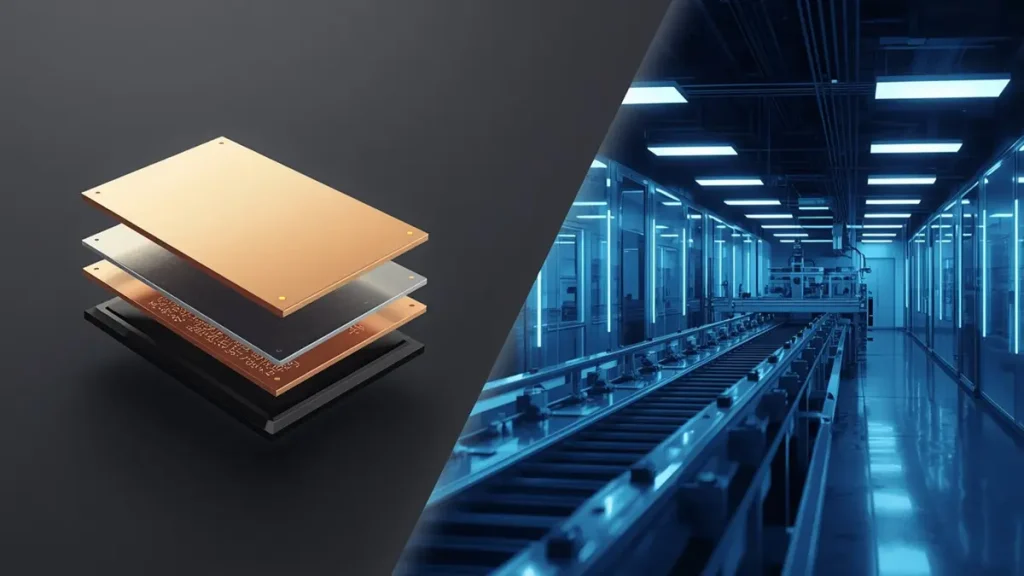
Immersion Gold PCB (ENIG) Layer Structure & Manufacturing Line – Hongda Circuit
The ENIG process sequence begins with copper surface activation, followed by electroless nickel deposition via autocatalytic reduction. The board then enters an immersion gold bath where gold ions displace nickel atoms at the surface. This displacement reaction is self-limiting—once the nickel is fully covered, gold deposition stops—ensuring consistent thickness regardless of pad geometry.
At our Shenzhen facility, we utilize HX Automated Plating Lines with real-time bath monitoring. Gold thickness is verified non-destructively via XRF on every production lot. Our process upgrade introduced closed-loop chemical filtration, reducing particulate contamination that historically contributed to black pad risk. The result is a surface finish that supports both SMT soldering and low-cycle electrical contact applications on the same board.
For buyers evaluating immersion gold PCB suppliers, process traceability matters more than price. A qualified manufacturer should provide nickel and gold thickness reports per IPC-4552A, along with solder wetting angle data. Read the Complete Guide →
Decision: Choosing the Right Gold Surface Finish for Your Application
ENIG vs Hard Gold vs ENEPIG: A Procurement Framework
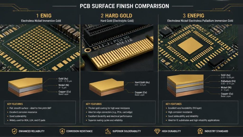
PCB Surface Finish Comparison Diagram: ENIG vs Hard Gold vs ENEPIG Specifications – Hongda Circuit
Selecting between ENIG, hard gold (electrolytic gold), and ENEPIG is the most consequential surface finish decision in PCB procurement. Each technology serves fundamentally different functions, and misapplication drives field failures or unnecessary cost inflation.
ENIG (Immersion Gold PCB) is optimized for solderability. Its pure gold layer (99.9%) and flat surface make it ideal for SMT pads, BGA footprints, and fine-pitch QFN devices. It is not designed for mechanical wear. If your design includes edge connectors or gold fingers subjected to repeated insertion cycles, ENIG will fail prematurely.
Hard Gold PCB (electroplated gold alloyed with 0.1–0.3% cobalt or nickel) is engineered for wear resistance. At 130–200 HK hardness and thicknesses of 0.25–2.5 µm, hard gold survives 1,000+ insertion cycles. This finish is mandatory for edge connectors, keypad contacts, and press-fit interfaces. However, hard gold must never be specified on SMT pads—its alloying elements oxidize during reflow, degrading solder joint strength.
ENEPIG PCB (Electroless Nickel / Electroless Palladium / Immersion Gold) adds a 0.1–0.25 µm palladium barrier between nickel and gold. This eliminates black pad risk entirely and enables both gold wire bonding and aluminum wire bonding on the same surface used for SMT assembly. For ASIL-D automotive modules, aerospace flight computers, or medical implants, ENEPIG is increasingly the specification-mandated choice.
At Hongda Circuit, we manufacture all three finishes under one roof. Our recommendation to procurement teams is simple: specify ENIG for soldering, hard gold for connectors, and ENEPIG when zero-defect reliability is non-negotiable. Read the Complete Guide →
When to Specify Immersion Gold PCB in Your BOM
ENIG is the correct specification when your design meets four criteria: (1) fine-pitch SMT components ≤0.5 mm pitch; (2) requirement for flat coplanar surfaces to ensure BGA ball uniformity; (3) medium-to-high volume production where OSP’s limited rework tolerance is insufficient; and (4) boards that must survive 3–5 reflow cycles including double-sided assembly.
Conversely, do not specify ENIG for applications requiring wire bonding (use ENEPIG), for ultra-low-cost consumer products where OSP suffices, or for through-hole-heavy power boards where HASL provides superior solderability on large thermal pads. Our engineering team at Shenzhen Hongda Circuit reviews over 200 BOMs monthly; the most common sourcing error we correct is ENIG overspecification on boards that only need OSP, inflating unit cost by $0.50–$0.80 per board unnecessarily.
For AI server PCB and 5G telecommunications hardware, ENIG remains the dominant finish in due to its compatibility with ultra-low-loss materials (Megtron 7/8, RO4350B) and its excellent planarity for 0.4 mm pitch BGA packages. Read the Complete Guide →
Cost Analysis: Immersion Gold PCB Pricing
Gold pricing volatility directly impacts ENIG PCB cost. ENIG adds approximately $0.50–$0.80 per board for a standard 100 mm × 100 mm, 4-layer PCB. ENEPIG carries a 20–35% premium ($0.65–$1.10) due to palladium material costs. Hard gold is area-dependent and can increase board cost by 15–30% depending on plating coverage.
The real cost consideration is total cost of ownership. A black pad field failure costs $50–$200 per board in rework and logistics. ENEPIG’s $0.15–$0.30 premium eliminates this risk. Similarly, specifying selective hard gold only on connector fingers—while keeping the remainder ENIG—optimizes cost without compromising wear performance.
At Hongda Circuit, we provide hybrid surface finish solutions: ENIG across the board with selective hard gold on gold fingers. This approach, common in telecom backplanes and industrial controllers, reduces gold consumption by up to 60% versus full-board hard gold while meeting IPC-4556 insertion cycle requirements. Read the Complete Guide →
Engineering: Technical Specifications and Quality Control
IPC-4552A Standards and Black Pad Prevention
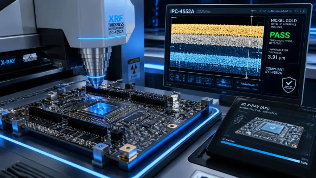
IPC-4552A ENIG Quality Inspection: XRF Thickness Measurement & 3D X-Ray Inspection – Hongda Circuit
IPC-4552A is the governing specification for ENIG deposits. It mandates nickel thickness of 3–6 µm, gold thickness of 0.05–0.23 µm, and mid-phosphorus nickel (6–9% P) to minimize black pad susceptibility. Black pad—a latent interfacial fracture at the nickel-gold boundary caused by hyper-corrosion during gold displacement—remains ENIG’s primary failure mode.
Prevention requires disciplined process control. At Shenzhen Hongda Circuit, our ENIG lines enforce:
- Bath MTO (Metal Turnover) limits to prevent gold bath contamination
- Mid-phosphorus nickel chemistry (7–8% P) for optimized grain structure
- Post-immersion gold bake cycles verified per lot
- 100% 3D X-Ray (AXI) inspection to detect micro-voids invisible to standard AOI
Our internal yield data shows black pad incidence below 5 PPM on qualified production lots—compared to industry averages of 50 PPM on uncontrolled lines. For automotive and medical customers, we offer ENEPIG as a zero-black-pad alternative, backed by IPC-4556 palladium thickness certification. Read the Complete Guide →
Gold Finger PCB Design and Manufacturing
Gold fingers (edge connector contacts) require hard gold plating, not ENIG. IPC standards specify 30–50 µin (0.76–1.27 µm) gold thickness for commercial applications, and 50–100 µin for IPC Class 3 or military/aerospace programs. The underlying nickel underplate must be 100–150 µin minimum to prevent copper diffusion into the gold layer.
Designing for gold finger manufacturing requires electrical connectivity during plating. PCB layouts must include plating buses (thieving lines) that connect all gold finger pads to a common cathode. These traces are removed after plating, but their placement affects panelization efficiency and scrap rates.
Hongda Circuits production lines support gold finger plating up to 120 µin with cobalt-hardened gold alloy. Our SCREEN Ledia LDI Exposure System ensures ±25 µm alignment accuracy between solder mask openings and gold finger edges—critical for preventing solder mask bleed onto contact surfaces that causes insertion force variability. We also provide beveled edge machining at 20°–45° angles to ease connector mating. Read the Complete Guide →
Material Compatibility: ENIG on High-Frequency and HDI Substrates
The electronics landscape demands ENIG compatibility with advanced substrates. For 224G PAM4 AI server backplanes, we plate ENIG directly onto Panasonic Megtron 7 (Dk 3.37, Df 0.0020) and Isola Tachyon 100G materials. The ultra-smooth ENIG surface (Ra <0.3 µm) minimizes skin effect losses at 56 GHz+ frequencies.
For Any-Layer HDI PCB with mSAP (Modified Semi-Additive Process) technology, ENIG deposits uniformly over sub-20 µm line/space geometries. Our mSAP lines achieve 10 µm trace width with ENIG coverage, supporting semiconductor test substrate and mobile device applications where immersion gold planarity is non-negotiable.
Rigid-flex PCB assemblies present unique challenges: gold plating on polyimide flex layers requires specialized adhesion promoters and stress-relief coverlay tapering at rigid-to-flex transitions. Hongda Circuit’s aerospace rigid-flex programs integrate ENIG on LCP (Liquid Crystal Polymer) and modified PI films for 5G millimeter-wave and satellite Ku/Ka-band applications. Read the Complete Guide →
Evidence: Why Procurement Teams Choose Hongda Circuit for Immersion Gold PCB
Certified Quality Systems and Real-Time Traceability
Shenzhen Hongda Circuit Technology Co., Ltd. operates under ISO 9001, IATF 16949, ISO 13485, and UL certifications. Our ENIG process is qualified to IPC-4552A with full lot traceability—from raw material batch numbers through press cycles, impedance testing, and final XRF thickness verification.
Our AI-driven ERP tracking system provides customers with real-time order visibility. Every immersion gold PCB lot includes a Certificate of Conformance documenting nickel thickness, gold thickness, phosphorus content, and solder wetting angle. For automotive OEMs, we maintain AS9102-style material traceability records meeting full supply chain audit requirements.
Advanced Equipment for Gold Surface Finish Manufacturing
Our Shenzhen Digital Twin Factory houses equipment specifically selected for precision surface finish control:
| Process Step | Equipment | Capability |
|---|---|---|
| LDI Imaging | SCREEN Ledia LDI Exposure | ±5 µm pad registration |
| Laser Drilling | Mitsubishi UV/CO₂ Laser | 25 µm microvia diameter |
| Layer Pressing | LAUFFER Lamination System | ±25 µm interlayer alignment |
| Electroless Plating | HX Automated ENIG Line | Real-time bath chemistry monitoring |
| Thickness Verification | XRF Spectrometry | Non-destructive Au/Ni measurement |
| Structural Inspection | Nordson DAGE 3D X-Ray (AXI) | 100% micro-void detection |
This equipment ecosystem enables us to deliver ENIG, ENEPIG, and selective hard gold on the same production panel—eliminating the need for customers to split orders across multiple suppliers.
From Prototype to Volume: Flexible Procurement Models
Hongda Circuit supports No-MOQ prototype orders with 24-hour DFM feedback, scaling to mid-volume campaigns without re-qualification. Our typical lead time for 4-layer ENIG prototypes is 5–7 days; for high-layer-count (40+ layers) with selective hard gold, 10–14 days. The 30-minute inquiry response and 1-hour engineering evaluation ensure procurement teams receive actionable quotes, not automated estimates.
We treat every project with equal priority regardless of scale. Whether you need 5 pieces for medical device validation or 50,000 pieces for consumer electronics mass production, our immersion gold PCB process parameters remain locked via automated recipe management—no manual adjustments that introduce batch-to-batch variation.
Ready to source your next ENIG PCB project? Submit your Gerber files to sales@pcbkr.com for a complimentary DFM review, XRF thickness simulation, and competitive quotation. Our engineering team will validate your surface finish selection against your application requirements, ensuring you specify exactly what your product needs—nothing more, nothing less.
FAQ: Immersion Gold PCB Procurement
What is the difference between immersion gold (ENIG) and hard gold on PCBs?
ENIG (immersion gold) is a chemically deposited thin gold layer (0.05–0.10 µm) over electroless nickel, designed for solderability and flatness on SMT pads. Hard gold is an electroplated gold-cobalt alloy (0.25–2.5 µm) engineered for mechanical wear resistance on edge connectors and gold fingers. ENIG cannot survive repeated insertion cycles; hard gold cannot be reliably soldered. AtHongda Circuit, we offer both finishes and recommend hybrid configurations (ENIG board + selective hard gold fingers) for cost-optimized designs.
How do I prevent black pad defects when sourcing ENIG PCBs?
Black pad is caused by excessive nickel corrosion during the immersion gold displacement reaction. Prevention requires: (1) mid-phosphorus nickel (7–9% P) chemistry; (2) controlled gold bath metal turnover (MTO); (3) supplier qualification to IPC-4552A; and (4) XRF thickness verification per lot. Shenzhen Hongda Circuit maintains black pad incidence below 5 PPM through closed-loop chemical filtration and real-time process monitoring. For zero-risk applications, we recommend ENEPIG, which uses a palladium barrier to eliminate nickel attack entirely.
What is the shelf life of an immersion gold PCB, and how should it be stored?
Properly packaged ENIG PCBs have a 12-month shelf life per IPC-4552A when stored in moisture barrier bags (MBB) at <25°C and <60% RH. ENEPIG extends this to 24+ months. After opening, boards should be processed within 72 hours or re-baked at 120°C for 4 hours to remove moisture absorption. For long-lead-time defense or automotive programs, specify ENEPIG or request vacuum-sealed storage with desiccant and humidity indicator cards.
How much does ENIG surface finish cost compared to OSP or HASL?
In 2026, ENIG adds approximately $0.50–$0.80 per board versus HASL for a standard 4-layer design. OSP is the cheapest at roughly $0.05–$0.15 per board but offers only 3–6 months shelf life and poor rework tolerance. ENEPIG costs 20–35% more than ENIG. Hard gold is area-dependent and typically adds 15–30% to total board cost. The optimal choice depends on component pitch, insertion cycle requirements, and reliability class—not price alone.
Can Chinese PCB manufacturers meet IPC Class 3 and automotive ENIG standards?
Yes. Leading Chinese manufacturers including Shenzhen Hongda Circuit Technology Co., Ltd. hold ISO 9001, IATF 16949, ISO 13485, and UL certifications with processes qualified to IPC-4552A and IPC-4556. The critical factor is not geography but documented process control: request XRF thickness reports, black pad prevention protocols, and material traceability records. Hongda Circuit provides full AS9102-style documentation and welcomes third-party audits. Our 2026 facility upgrade introduced AI-driven AOI and 100% 3D X-Ray inspection, matching or exceeding capabilities of Western tier-1 suppliers.
About Author
David Chen https://www.linkedin.com/in/pcbcoming
David Chen boasts an extensive professional background in PCBA manufacturing, PCBA testing, and PCBA optimization, with specialized expertise in high-precision PCBA fault analysis and rigorous PCBA reliability testing. The author has worked with high-layer-count server PCB fabrication, ultra-low-loss backplane stackups, and thermo-mechanical reliability optimization for AI infrastructure projects involving 112G and 224G PAM4 architectures. Skilled in complex circuit design and cutting-edge advanced PCB manufacturing processes, he delivers solutions that elevate product durability and performance across industrial applications. His technical articles focusing on PCBA manufacturing workflows and testing methodologies are widely cited by industry peers, research institutions, and technical platforms, solidifying his reputation as a recognized technical authority in the global circuit board manufacturing sector.