What Is Immersion Gold PCB (ENIG)? Chemical Process, Shelf Life & Black Pad Prevention
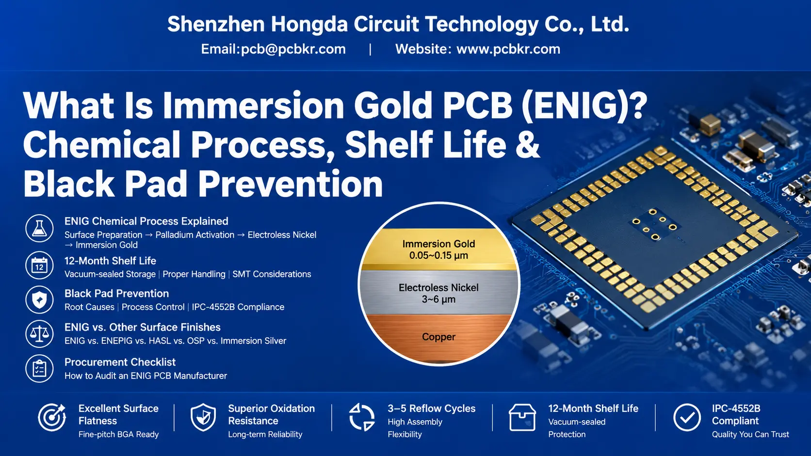
Quick Engineering Definition: ENIG (Electroless Nickel Immersion Gold) is a dual-layer metallic surface finish for printed circuit boards, consisting of 3–6 µm of electroless nickel-phosphorus alloy capped by 0.05–0.15 µm of immersion gold. It delivers exceptional surface flatness for fine-pitch QFP and BGA assembly, superior oxidation resistance, and a 12-month shelf life under vacuum-sealed storage. For hardware engineers and procurement managers evaluating PCB surface finish options, ENIG remains the most widely adopted mid-to-high-reliability solution in North American and European supply chains.
The ENIG Chemical Reaction Process Explained
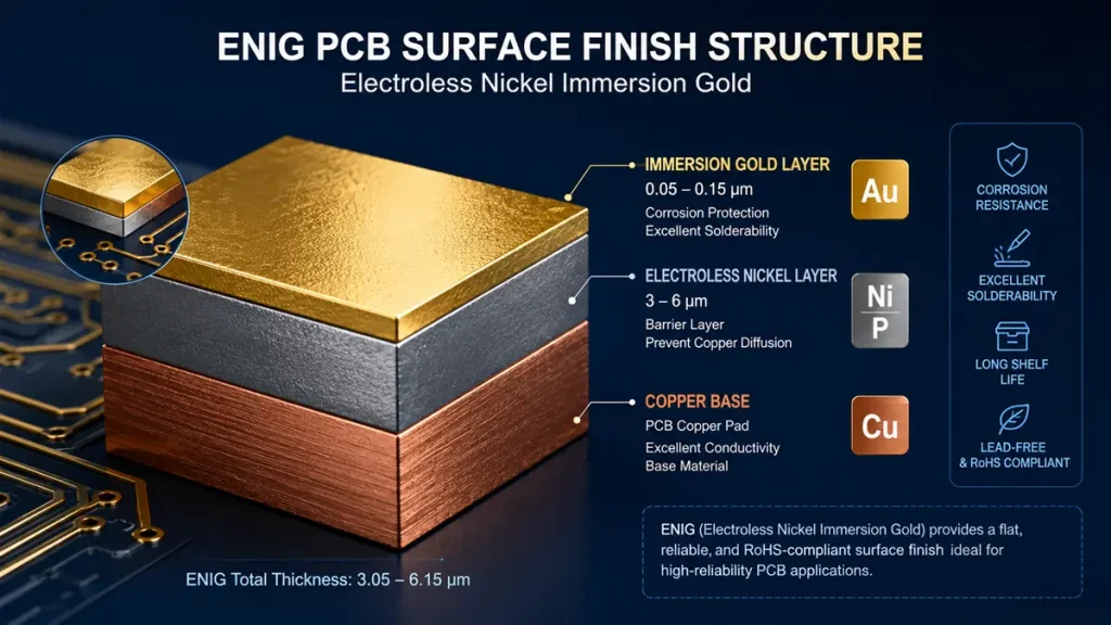
ENIG PCB Surface Finish Layer Structure & Thickness Specifications
Understanding the wet-chemistry sequence behind ENIG plating is essential for procurement teams auditing supplier capabilities and for process engineers troubleshooting solderability issues. The entire process occurs in an automated horizontal or vertical conveyorized line, with each bath operating under tightly controlled temperature, pH, and dwell-time windows.
Step 1: Surface Preparation and Micro-Etching
Before any metal deposition occurs, the bare copper pads must be chemically cleaned and micro-roughened. A sulfuric acid–peroxide micro-etch removes approximately 1.0–1.5 µm of surface copper, creating a micro-rough topography that enhances mechanical adhesion for the subsequent nickel layer. At Shenzhen Hongda Circuit Technology Co., Ltd., this stage is monitored by automated chemical dosing systems that maintain etch-rate consistency within ±5% across 24″ × 18″ production panels.
Step 2: Palladium Activation
The cleaned copper surface is immersed in a palladium-tin colloidal activator. Palladium nanoparticles adsorb onto the copper, serving as catalytic nucleation sites for the electroless nickel reaction that follows. Without uniform palladium seeding, nickel deposition becomes patchy, leading to skip-plating defects that are invisible to AOI but catastrophic during reflow. Leading ENIG PCB manufacturers now employ proprietary activator formulations with extended bath life and reduced tin residue, minimizing the risk of intermetallic contamination.
Step 3: Electroless Nickel Deposition (Autocatalytic Plating)
This is the structural heart of the ENIG finish. The panel enters an 80°C–85°C alkaline nickel bath containing nickel sulfate, sodium hypophosphite (reducing agent), and complexing agents. The hypophosphite decomposes on the palladium-catalyzed copper surface, reducing nickel ions to metallic nickel while co-depositing 7–10% phosphorus by weight.
The phosphorus content is not incidental—it determines the entire reliability profile of the finished board:
- 7–9% phosphorus (mid-phosphorus): Optimal balance of corrosion resistance and solderability. This is the IPC-4552B sweet spot and the specification enforced by high-reliability ENIG PCB suppliers.
- <7% phosphorus: Excessive magnetic properties and reduced corrosion resistance; rarely used in modern ENIG plating.
- 11% phosphorus: High corrosion resistance but brittle; grain-boundary phosphorus accumulation increases black pad susceptibility.
At Hongda Circuit, the nickel bath is analyzed every four hours by titration and X-ray fluorescence (XRF) spectroscopy, with phosphorus content locked between 7.5% and 8.5%. Bath metal turnover (MTO) is capped at six cycles to prevent phosphorus drift, a discipline that separates premium ENIG PCB manufacturers from commodity shops.
Step 4: Immersion Gold Deposition (Galvanic Displacement)
In the final bath, the nickel-coated panel is immersed in a mildly acidic gold solution (pH 4.5–5.5, 80°C–85°C). Gold ions (Au+) undergo a spontaneous redox displacement reaction with surface nickel atoms:
2Au+ + Ni → 2Au + Ni2+
Gold deposits atom-by-atom until the surface nickel is fully passivated, forming a self-limiting layer typically 0.05–0.10 µm (2–4 µin) thick. The reaction is inherently self-terminating—once the nickel surface is sealed by gold, displacement stops. However, if the gold bath is over-concentrated, overly acidic, or dwell time exceeds 8–12 minutes, the displacement reaction becomes aggressive and attacks nickel grain boundaries. This hyper-corrosion is the root cause of black pad syndrome.
Modern ENIG plating lines integrate real-time bath conductivity and pH sensors with automated dosing pumps, maintaining gold displacement within the IPC-4552B envelope. At Shenzhen Hongda Circuit Technology Co., Ltd., gold thickness is verified on every production lot using non-destructive XRF, with statistical process control (SPC) charts tracking Cpk values >1.33.
ENIG Shelf Life, Storage Guidelines & SMT Assembly Considerations
Realistic Shelf Life and Vacuum Packaging Standards
A properly processed ENIG surface finish provides a 12-month shelf life when boards are vacuum-sealed with desiccant and humidity indicator cards (HIC) in moisture-barrier bags (MBB). This exceeds OSP (3–6 months) and matches lead-free HASL, making ENIG the preferred finish for long-lead-time programs common in industrial, automotive, and defense procurement cycles.
Critical storage parameters:
- Temperature: <25°C (77°F)
- Relative Humidity: <60% RH
- Packaging: Vacuum-sealed MBB with silica desiccant and HIC
If boards are exposed to ambient air for more than 168 hours (7 days) before SMT reflow, a bake-out cycle is mandatory: 120°C for 4 hours to remove absorbed moisture and prevent delamination during reflow. Procurement managers should verify that their ENIG PCB supplier documents bake-out protocols and provides time-stamped vacuum-seal certificates with each shipment.
SMT Reflow Profile and Solderability Performance
ENIG is uniquely tolerant of multiple thermal excursions. A well-controlled ENIG finish withstands 3–5 reflow cycles without solderability degradation, making it ideal for double-sided complex SMT assemblies, rework operations, and mixed-technology boards (SMT + through-hole + wave solder).
Recommended solder paste and flux pairings:
- SAC305 or SAC307 lead-free solder paste: Standard for RoHS-compliant assemblies
- No-clean synthetic flux: Compatible with ENIG’s non-reactive gold surface; eliminates post-reflow cleaning while maintaining ionic cleanliness <1.56 µg NaCl eq/cm² per IPC-TM-650
Wetting balance testing per IPC J-STD-003 should show a wetting force curve reaching 90% of maximum within 2.0 seconds at 245°C. If wetting is delayed, the gold layer may be contaminated with organic residues from the plating bath—a defect that visual inspection cannot catch but that will cause balling and opens during BGA assembly.
Root Cause and Prevention of Black Pad and Gold Embrittlement
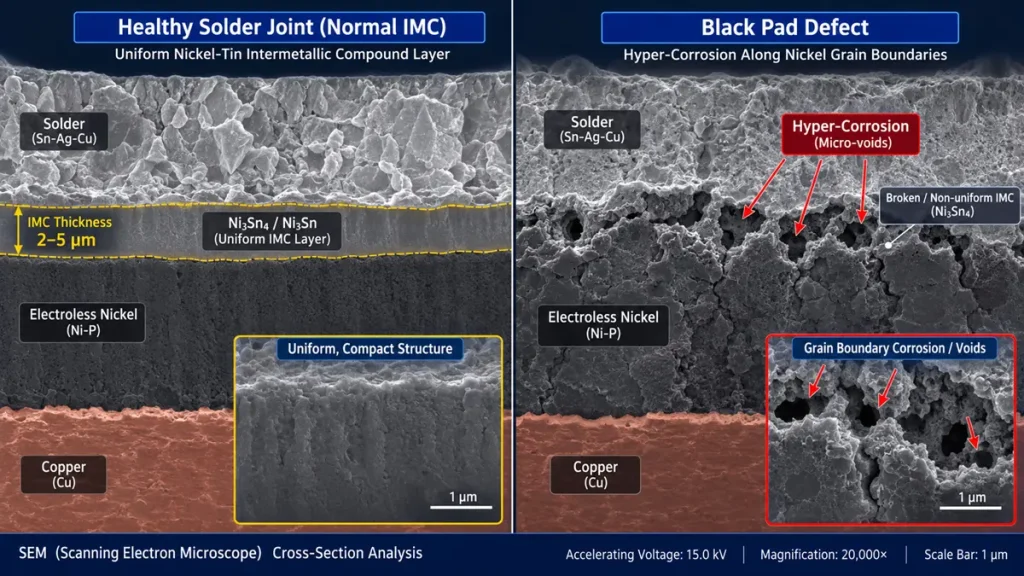
SEM Cross-Section Analysis: Healthy ENIG Solder Joint vs Black Pad Defect
Understanding Black Pad: Hyper-Corrosion of the Nickel Layer
Black pad is an interfacial corrosion defect occurring at the nickel-gold boundary during immersion gold plating. When the gold displacement reaction is overly aggressive, it preferentially attacks phosphorus-rich grain boundaries in the electroless nickel, leaving behind a dark, non-solderable nickel-phosphorus corrosion layer. The defect is latent and invisible: standard visual inspection, AOI, and X-ray cannot detect it. It manifests only after thermal cycling as brittle BGA ball fractures, often 500–2,000 cycles into field operation.
Primary root causes of black pad in ENIG PCB manufacturing:
- Over-active immersion gold bath: Excessive gold concentration or low pH accelerates nickel corrosion.
- Extended dwell time: Gold immersion beyond 8–12 minutes allows hyper-corrosion to propagate deep into grain boundaries.
- Phosphorus content drift: Nickel bath aging pushes phosphorus outside the 7–9% window; high phosphorus (>10%) concentrates at boundaries.
- Acidic bath contamination: Sulfate or chloride ingress from upstream rinses destabilizes the displacement kinetics.
Prevention and quality controls enforced by top-tier ENIG PCB suppliers:
| Control Parameter | Target Specification | Verification Method |
|---|---|---|
| Nickel phosphorus content | 7.5–8.5% by weight | Titration + XRF coupon analysis |
| Gold bath pH | 4.5–5.5 | Automated inline pH probe |
| Gold immersion dwell time | 6–10 minutes | PLC-controlled conveyor speed |
| Gold thickness | 0.05–0.10 µm (2–4 µin) | XRF per IPC-4552B |
| Nickel bath MTO limit | ≤6 cycles | Bath log with lot traceability |
| Corrosion evaluation | IPC-4552B statistical sampling | Cross-sectional SEM on test coupons |
IPC-4552B (Revision B, 2022) introduced a critical evolution from its predecessor: instead of rejecting an entire batch for a single Level 3 corrosion spike, it mandates statistical sampling across multiple pads. This prevents false-positive scrap while still catching systemic black pad risks. Procurement managers should demand IPC-4552B compliance documentation—not Rev A—from their ENIG PCB manufacturer.
Mitigating Gold Embrittlement in SMT Soldering
Gold embrittlement occurs when excessive gold thickness (>0.15 µm / 5 µin) dissolves into the solder joint during reflow, forming brittle AuSn4 intermetallic compounds (IMC). Under mechanical shock or thermal cycling, these IMC layers fracture, causing catastrophic joint failure.
The prevention is straightforward but requires supplier discipline: keep immersion gold thickness under 0.15 µm. This is not a suggestion—it is an IPC-4552B requirement. At Hongda Circuit, automated XRF thickness verification is performed on every panel, with out-of-spec boards automatically routed to rework or scrap. For mission-critical applications (automotive ASIL-D, medical Class III, aerospace IPC Class 3), specifying ENEPIG (Electroless Nickel Electroless Palladium Immersion Gold) eliminates both black pad and gold embrittlement risks by introducing a palladium diffusion barrier.
ENIG vs. Other PCB Surface Finishes: A Procurement Decision Matrix
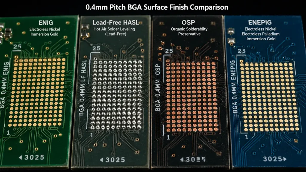
0.4mm Pitch BGA PCB Surface Finish Comparison: ENIG vs Lead-Free HASL vs OSP vs ENEPIG
Hardware engineers and procurement managers do not select surface finishes in a vacuum. The choice must balance cost, reliability, assembly complexity, and supply chain constraints. The following matrix provides a defensible framework for ENIG finish selection against alternatives.
| Parameter | ENIG | ENEPIG | Lead-Free HASL | OSP | Immersion Silver |
|---|---|---|---|---|---|
| Surface Flatness | Excellent (<0.5 µm) | Excellent (<0.5 µm) | Poor (±15 µm) | Excellent | Excellent |
| Shelf Life | 12 months | 24+ months | 12 months | 3–6 months | 6–12 months |
| Fine-Pitch BGA Suitability | ≤0.4 mm pitch | ≤0.4 mm pitch | >0.5 mm pitch | ≤0.5 mm pitch | ≤0.5 mm pitch |
| Reflow Cycles | 3–5 cycles | 6+ cycles | 3+ cycles | 1–2 cycles | 2–3 cycles |
| Wire Bonding | No (brittle) | Yes (Au + Al) | No | No | Limited |
| Black Pad Risk | Present (controlled) | None | N/A | N/A | N/A |
| Relative Cost | $$$ ($0.50–$0.80 per 100×100mm 4L) | $$$$ ($0.65–$1.10) | $ ($0.10–$0.20) | $ ($0.05–$0.15) | $$ ($0.20–$0.35) |
| Best Use Case | Fine-pitch SMT, general high-reliability | Automotive, medical, wire bond, zero-defect | Through-hole, power, low-cost consumer | High-volume consumer, single reflow | RF/high-frequency, 5G mmWave |
When ENIG Is the Right Choice
Specify ENIG surface finish when your design includes:
- Fine-pitch BGA or CSP packages at 0.4–0.5 mm pitch
- Double-sided SMT requiring 3+ reflow cycles
- Shelf-life requirements of 6–12 months
- Need for a solderable surface that also functions as a low-cycle contact/test point
- Budget constraints that make ENEPIG’s 20–35% premium unjustified
When to Upgrade to ENEPIG Instead of Standard ENIG
Upgrade to ENEPIG when your program demands:
- Gold or aluminum wire bonding on the same board as SMT
- Zero black pad tolerance (automotive ASIL-C/D, medical implant, aerospace)
- More than 5 reflow cycles or extended thermal cycling (-40°C to +125°C per IPC-9701)
- Shelf life exceeding 12 months (spare parts, long-lead defense programs)
- Mixed assembly: SMT + wire bond + press-fit connectors
The ENEPIG premium of approximately $0.15–$0.30 per board is immediately recovered if it prevents a single field failure requiring rework at $50–$200 per unit.
How to Audit an ENIG PCB Manufacturer: A Procurement Checklist
Selecting an ENIG PCB supplier is not a commodity decision. The difference between a qualified ENIG line and a marginal one is the difference between 99.7% first-pass yield and catastrophic field failures. Use this checklist when vetting ENIG PCB manufacturers in China, North America, or Europe.
1. Demand IPC-4552B Process Documentation
Request the following with every quotation and production lot:
- Batch-specific XRF thickness reports (nickel and gold)
- Nickel bath phosphorus analysis (target: 7–9%)
- Gold bath pH and temperature logs
- Metal turnover (MTO) records for the nickel bath
- Cross-sectional SEM corrosion evaluation per IPC-4552B statistical criteria
At Shenzhen Hongda Circuit Technology Co., Ltd., these documents are generated automatically by our manufacturing execution system (MES) and delivered as PDF traceability packets with each shipment. No report, no shipment.
2. Verify In-House Analytical Equipment
A fabricator without in-house XRF cannot control ENIG thickness in real time. Verify that your supplier operates:
- XRF thickness analyzer: Non-destructive verification of Ni and Au layers
- Cross-sectional grinding/polishing station: For SEM corrosion analysis
- Wetting balance tester: Per IPC J-STD-003 solderability validation
- Ionic contamination tester: Omega meter or ion chromatography
Hongda Circuit maintains a full analytical laboratory including XRF, SEM, wetting balance, and ion chromatography, ensuring ENIG quality is verified internally before boards reach your incoming QC.
3. Evaluate Equipment and Process Control Infrastructure
Modern ENIG plating demands precision beyond manual chemistry. Look for:
- Automated chemical dosing systems: Eliminates human error in bath maintenance
- Inline pH/conductivity/temperature sensors: Real-time process monitoring
- PLC-controlled conveyor speeds: Dwell-time accuracy within ±10 seconds
- Class 1000 or better cleanroom environment: Prevents particulate contamination
Our ENIG line at Shenzhen Hongda Circuit Technology Co., Ltd. integrates automated dosing, inline monitoring, and SPC charting. The plating line is housed in a temperature-controlled cleanroom environment, with laminar airflow preventing airborne particulate from settling on wet panels between baths.
4. Confirm Certification Alignment
For ENIG PCB procurement in regulated industries, certifications are non-negotiable:
- ISO 9001: Quality management system baseline
- IATF 16949: Automotive supplier quality requirements
- AS9100D: Aerospace and defense quality standard
- IPC-6012 Class 3: High-reliability PCB performance specification
- UL recognition: Flammability and safety compliance
Shenzhen Hongda Circuit Technology Co., Ltd. holds ISO 9001, IATF16949, AS9100D, and UL certifications, with full production lot traceability from raw laminate to finished board.
5. Assess Advanced Capability Integration
If your program involves HDI, high-frequency, or AI server applications, ensure your ENIG supplier can handle the full technology stack—not just the surface finish. Hongda Circuit’s 2026 capability portfolio includes:
- Up to 40-layer production-qualified multilayer boards
- Any-layer HDI with 40 µm / 40 µm trace/space
- Laser microvias down to 50 µm via UV-YAG systems
- Controlled impedance: ±5% standard, ±3% premium track
- 224G PAM4 signal integrity validation with in-house VNA to 67 GHz
- VIPPO (Via-in-Pad Plated Over) with ENIG/ENEPIG capping for 0.3 mm pitch BGA
By consolidating ENIG plating with advanced HDI and high-speed capabilities under one roof, Hongda Circuit eliminates the cross-factory handoff risks that introduce plating contamination and misalignment defects.
2026 ENIG Technology Trends: What Procurement Managers Should Know
The ENIG landscape is evolving rapidly. Three trends are reshaping supplier selection criteria in 2026:
1. AI-Driven Process Monitoring
Leading ENIG chemical suppliers and PCB manufacturers are integrating machine-learning algorithms with plating-line sensors. Real-time bath chemistry prediction reduces phosphorus drift and gold bath instability by 40–60% compared to scheduled manual analysis. When auditing suppliers, ask whether their MES supports predictive chemistry alerts.
2. Eco-Friendly, Low-Toxicity Chemistries
Driven by REACH and RoHS evolution, next-generation ENIG baths are shifting toward water-based, low-cyanide, and biodegradable formulations. MacDermid Alpha and Atotech launched compliant chemistries in 2024–2025 that match traditional performance while reducing hazardous waste by 30%. Procurement teams with corporate sustainability mandates should prioritize suppliers using green ENIG chemistry.
3. Ultra-Thin Gold for High-Frequency 5G and AI Applications
At 56 GHz (224G PAM4 Nyquist frequency), even 0.10 µm of gold introduces measurable skin-effect losses. Emerging ENIG formulations target 0.03–0.05 µm gold thickness with enhanced nickel corrosion resistance, trading solderability margin for signal integrity. For 5G mmWave and AI backplane designs, discuss ultra-thin ENIG specifications with your fabricator.
Frequently Asked Questions: ENIG PCB Procurement
How do I verify that my ENIG PCB supplier is actually controlling black pad risk, not just claiming IPC-4552B compliance?
Demand three documents before placing your first order: (a) a recent cross-sectional SEM report showing nickel corrosion levels per IPC-4552B statistical criteria, (b) six months of nickel bath phosphorus titration records demonstrating control within 7–9%, and (c) XRF thickness Cpk data showing gold thickness process capability ≥1.33. A supplier who cannot produce these within 24 hours is not controlling the process—they are hoping for the best. At Hongda Circuit, we provide these reports as standard with every quotation.
What is the real cost difference between ENIG and ENEPIG, and when does ENEPIG pay for itself?
For a standard 100 mm × 100 mm four-layer board, ENIG adds approximately $0.50–$0.80 to bare board cost, while ENEPIG adds $0.65–$1.10. The $0.15–$0.30 ENEPIG premium pays for itself immediately if your design requires wire bonding (avoiding $1.50–$3.00 selective hard gold plating), if you are building automotive ASIL-D or medical Class III hardware where a single black pad field failure costs $50–$200 in rework, or if your program demands shelf life beyond 12 months.
Can I store ENIG-finished boards for more than 12 months, and what happens if I do?
ENIG shelf life is rated at 12 months under vacuum-sealed, desiccant-protected storage (<25°C, <60% RH). Beyond 12 months, the immersion gold layer remains intact, but micro-porosity in the gold film allows slow nickel oxidation beneath the surface. After 18–24 months, solderability degrades measurably—wetting times increase and solder paste may ball. For programs requiring 24+ month storage, specify ENEPIG (24+ month shelf life) or plan for incoming solderability re-qualification per IPC J-STD-003.
Why do some Chinese ENIG PCB suppliers quote significantly lower prices than others for the same ENIG specification?
Price variance in ENIG PCB manufacturing almost always traces to three hidden cost drivers: (1) Bath maintenance discipline—cheap suppliers extend nickel bath MTO beyond 8–10 cycles, causing phosphorus drift and black pad risk; (2) Gold thickness underspec—quoting 0.05 µm but delivering 0.03 µm saves gold cost but invites nickel oxidation; (3) Analytical equipment gaps—suppliers without in-house XRF outsource testing, creating 24–48 hour feedback loops during which defective lots ship. The lowest quote is rarely the lowest total cost of ownership when field failure risk is included.
What equipment and process capabilities should I look for when auditing a China-based ENIG PCB manufacturer for high-reliability programs?
Beyond the standard ENIG plating line, verify four capabilities: (1) In-house XRF and SEM for real-time thickness and corrosion verification; (2) Automated chemical dosing with inline pH/conductivity monitoring, not manual bucket additions; (3) Class 1000 cleanroom plating environment to prevent particulate skip-plating; (4) Full MES traceability with lot-linked bath logs, not paper records. Shenzhen Hongda Circuit Technology Co., Ltd. maintains all four, backed by AS9100D and IATF 16949 certification, making our ENIG line suitable for automotive, aerospace, and medical procurement programs.
Validate Your Gerber Files and Gold Thickness Requirements
Surface finish selection is a system-level decision that impacts solder joint reliability, signal integrity, and total program cost. Specifying ENIG without verifying your supplier’s process control infrastructure is equivalent to specifying a high-performance alloy without mill certification.
Shenzhen Hongda Circuit Technology Co., Ltd. provides a complete IPC-4552B compliance audit and complimentary DFM review within 24 hours of Gerber submission. Our engineering team validates stackup impedance, gold thickness feasibility, and black pad risk factors before tooling begins—eliminating surprises at first-article inspection.
Request a Free DFM File Check & ENIG Engineering Review →
Explore Our Advanced PCB Manufacturing Capabilities & Instant Quote →
Contact: sales@pcbkr.com
About Author
David Chen https://www.linkedin.com/in/pcbcoming
David Chen boasts an extensive professional background in PCBA manufacturing, PCBA testing, and PCBA optimization, with specialized expertise in high-precision PCBA fault analysis and rigorous PCBA reliability testing. The author has worked with high-layer-count server PCB fabrication, ultra-low-loss backplane stackups, and thermo-mechanical reliability optimization for AI infrastructure projects involving 112G and 224G PAM4 architectures. Skilled in complex circuit design and cutting-edge advanced PCB manufacturing processes, he delivers solutions that elevate product durability and performance across industrial applications. His technical articles focusing on PCBA manufacturing workflows and testing methodologies are widely cited by industry peers, research institutions, and technical platforms, solidifying his reputation as a recognized technical authority in the global circuit board manufacturing sector.