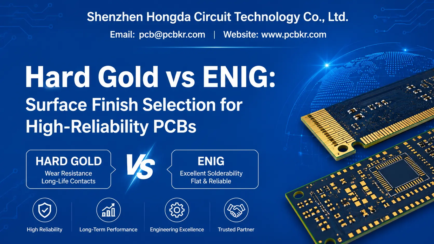
Hard Gold vs ENIG: Surface Finish Selection for High-Reliability PCBs
Why Surface Finish Selection Determines Product Lifecycle Costs
A PCB surface finish does more than prevent copper oxidation. It defines solder joint reliability, contact resistance stability, and mechanical durability across the product’s entire service life. Choose incorrectly, and you risk field failures ranging from BGA voiding to edge connector fretting corrosion. Choose correctly, and you optimize both assembly yield and long-term mean time between failures (MTBF).
For PCB Layout Engineers and Electronics Purchasing Managers, the debate typically narrows to two gold-based finishes: Electroless Nickel Immersion Gold (ENIG) and electrolytic Hard Gold. Both contain gold. Both protect copper. Yet they serve fundamentally different engineering functions. This guide breaks down the chemistry, mechanical properties, cost structures, and procurement criteria that should drive your specification—backed by 2026 manufacturing data from Shenzhen Hongda Circuit Technology Co., Ltd.
What Is ENIG? Chemistry, Structure, and Assembly Advantages
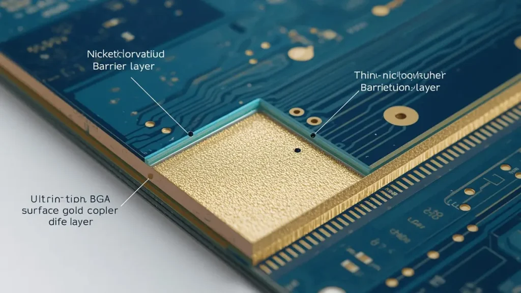
ENIG PCB Surface Finish Microscopic Cross-Section and Layer Structure Diagram
ENIG deposits an amorphous nickel-phosphorus (Ni-P) alloy layer—typically 3.0–6.0 µm thick—onto exposed copper pads through an autocatalytic chemical reduction process. A thin immersion gold layer (0.05–0.15 µm, or 2–5 µin) then displaces the nickel surface via galvanic exchange. The result is a dead-flat, solderable surface with no electrolytic current density variations.
ENIG Nickel-Phosphorus Barrier and Immersion Gold Deposition
The Ni-P layer functions as a diffusion barrier. During reflow, it prevents copper from migrating into the solder joint and forming brittle Cu₃Sn intermetallics. The immersion gold layer, being thin and soft (60–80 HV Vickers hardness), dissolves rapidly into molten solder, exposing the nickel for intermetallic bonding. This chemistry makes ENIG exceptionally compatible with fine-pitch QFN, BGA, and 0.4 mm pitch components where pad coplanarity directly impacts assembly yield.
At Shenzhen Hongda Circuit Technology, ENIG processing runs on automated electroless nickel lines with real-time bath monitoring. Phosphorus content stays within the 7–9 wt% window specified in IPC-4552B, minimizing black pad corrosion risk on large pads above 10 mm. XRF thickness verification occurs on production panels—not just test coupons—ensuring the gold layer falls within the 0.05–0.10 µm sweet spot for solderability.
When ENIG Becomes the Default Choice for Fine-Pitch SMT
Specify ENIG when your design includes:
- Fine-pitch SMT components (≤0.5 mm pitch)
- BGA or CSP packages requiring flat pad geometry
- Long shelf-life requirements (12–24 months stored properly)
- Aluminum wire bonding on small pads (with thickness ≥3–5 µin)
Do not specify ENIG for edge connectors, gold fingers, or any surface facing repeated mechanical contact. The immersion gold layer wears through in fewer than 100 insertion cycles, exposing the nickel underneath to oxidation and contact resistance spikes.
What Is Hard Gold? Electroplated Alloy Engineering for Contact Durability
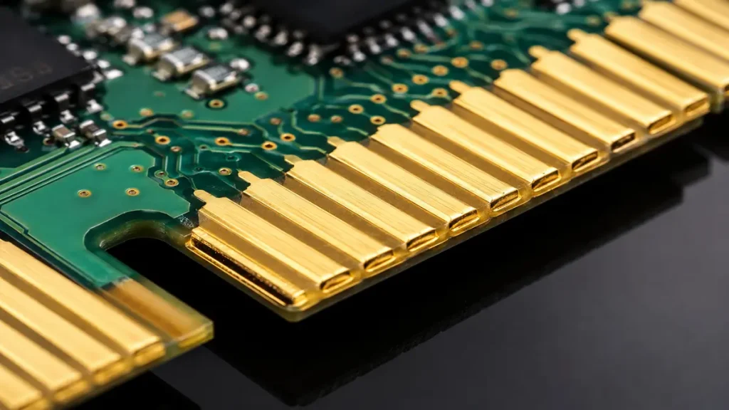
Macro Photograph of Electrolytic Hard Gold Plated PCB Edge Connector Fingers
Hard gold is an electrolytic deposit—not a chemical immersion. A DC current drives gold ions from a cyanide-based electrolyte onto a nickel underplate, with 0.1–0.5% cobalt or nickel added as a hardening agent. The resulting alloy achieves 130–200 HV Knoop hardness, roughly triple that of ENIG’s soft gold.
Cobalt-Hardened Gold and the Knoop Hardness Advantage
The cobalt addition transforms gold from a soft, ductile metal into a wear-resistant surface capable of surviving 1,000–10,000+ mating cycles. Hard gold thickness typically ranges from 30 µin (0.76 µm) for Class 2 commercial applications to 100 µin (2.54 µm) for aerospace and military connectors. This thickness—20 to 50 times greater than ENIG—provides the sacrificial wear volume needed for sliding, wiping, and insertion contact.
At Shenzhen Hongda Circuit Technology Co., Ltd., pulse-reverse electrolytic plating delivers thickness uniformity within ±8% across panels up to 24 inches. The sulfur-free nickel underplate measures 100–300 µin with organic contamination held below 100 ppm. This matters because sulfur residues embed into the gold lattice during plating, creating high-resistance sulfide films that degrade contact performance over time.
IPC-4556 Specifications for Gold Finger PCB Applications
IPC-4556 governs electrolytic hard gold for edge connectors. Key parameters include:
- Gold purity: Minimum 99.0% (Type I/II per MIL-G-45204)
- Hardness: 130–200 Knoop (or Vickers equivalent)
- Thickness by class: Class 2 (30 µin), Class 3 (50 µin), extended life (75–100 µin)
- Nickel underplate: 100–200 µin minimum for copper diffusion blocking
Shenzhen Hongda Circuit Technology certifies every gold finger batch to IPC-4556, with four-wire Kelvin contact resistance testing performed on 100% of production panels—not statistical samples.
Hard Gold vs ENIG: Head-to-Head Technical Comparison
| Property | Hard Gold (Electrolytic) | ENIG (Immersion) |
|---|---|---|
| Gold thickness | 0.76–2.54 µm (30–100 µin) | 0.05–0.15 µm (2–5 µin) |
| Hardness (Knoop) | 130–200 HK | 60–80 HK |
| Wear cycles | 1,000–10,000+ | <100 |
| Solderability | Poor—cobalt inhibits wetting | Excellent—thin gold dissolves instantly |
| Contact resistance | Stable (<10 mΩ variation) | Degrades rapidly under friction |
| Surface flatness | Slight edge buildup possible | Dead flat, ideal for fine-pitch |
| Cost per sq in | $1.50–$3.00 | $0.50–$1.00 |
Knoop Hardness and Wear Resistance Metrics
The 130–200 Knoop hardness of hard gold arises from cobalt atoms distorting the face-centered cubic gold lattice. This dislocation blocking prevents plastic deformation during connector mating. ENIG’s soft gold, by contrast, smears and transfers to the mating contact during the first few insertion cycles—a phenomenon called adhesive wear. Once the 2–5 µin gold film depletes, the exposed nickel-phosphorus layer oxidizes, driving contact resistance from milliohms to ohms.
Solderability and Contact Resistance Performance
ENIG dominates solderability because its thin gold layer dissolves completely into the solder joint within seconds of reflow, leaving a fresh nickel-tin intermetallic. Hard gold’s cobalt content reduces solder wetting force by 30–50% compared to pure gold, creating irregular fillets and potential voiding under BGAs. For this reason, hard gold should never cover SMT pads that will undergo primary reflow soldering.
Solder Embrittlement Risk: Why Hard Gold Is Not a Solder Finish
This is the specification error that destroys assemblies. When hard gold is soldered, the cobalt-hardened gold layer does not fully dissolve into the solder joint. Residual gold concentration above 3–4 wt% in the solder matrix creates AuSn₄ intermetallic compounds. These platelets precipitate at grain boundaries under thermal cycling, transforming ductile solder into brittle glass.
Cobalt Diffusion and Intermetallic Compound Formation
Cobalt further complicates the metallurgy. Unlike ENIG’s pure gold flash, hard gold’s cobalt alloying element stabilizes the gold layer against dissolution. During reflow, gold and cobalt migrate into the solder bulk at different rates, creating a chemically heterogeneous joint. The result: reduced shear strength, increased thermal fatigue susceptibility, and crack propagation under vibration.
IPC-J-STD-001 explicitly warns against soldering directly onto hard gold surfaces unless the gold is fully dissolved or removed. The safe approach? Keep hard gold restricted to connector contacts, and specify ENIG or ENEPIG for all solderable lands.
ENIG vs Hard Gold Cost Analysis: Beyond Per-Square-Inch Pricing
Purchasing managers often compare surface finishes by raw material cost. ENIG runs approximately $0.50–$1.00 per square inch. Hard gold commands $1.50–$3.00 per square inch—roughly 2× to 3× the ENIG baseline. But this headline comparison misses the total cost of ownership (TCO).
Gold Thickness, Processing Steps, and Total Cost of Ownership
Hard gold requires:
- Photoresist masking to define plating zones
- Electrolytic nickel strike and gold deposition
- Resist stripping and secondary cleaning
- Edge beveling (20°–45°) for connector insertion
- XRF thickness verification per IPC-4556
ENIG requires:
- Bulk panel processing (no masking for full-board ENIG)
- Electroless nickel bath immersion
- Immersion gold dip
- Standard XRF spot checks
However, specifying hard gold on an entire board when only the edge connector needs it is procurement malpractice. Selective hard gold plating—applying hard gold only to gold fingers while leaving SMT pads in ENIG—adds $0.50–$1.00 per board and 2–5 days to lead time. Yet it eliminates the catastrophic cost of field connector failures, warranty claims, and customer downtime.
At Shenzhen Hongda Circuit Technology, selective plating uses precision photolithography masking with 20–30 mil (0.5–0.75 mm) minimum spacing between finish zones. The electrolytic hard gold step occurs before solder mask application; ENIG chemistry follows afterward to protect exposed SMT pads. This sequencing prevents ENIG contamination of the hard gold surface while preserving solderability on component lands.
Engineering Selection Framework: ENIG, Hard Gold, or Selective Hard Gold?
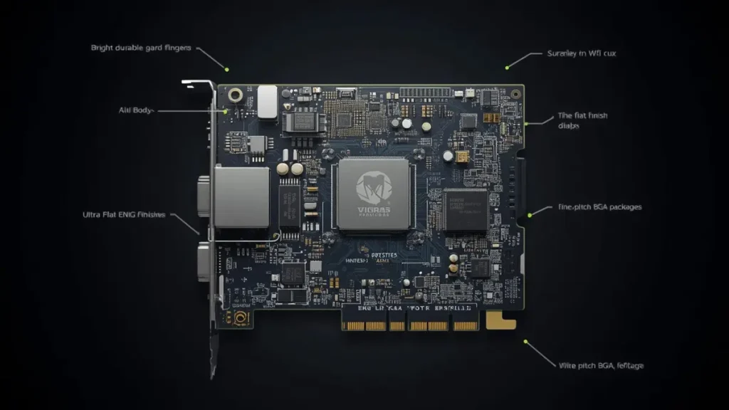
Top-Down Engineering View of Selective Hard Gold and ENIG Finish on AI Accelerator PCB
Use this decision tree to lock your specification before releasing fabrication drawings:
1. Does the board contain edge connectors or gold fingers?
- No → ENIG (or OSP/HASL for cost-sensitive designs)
- Yes → Proceed to Question 2
2. What is the expected insertion cycle count?
- <50 cycles, cost-critical consumer product → Thin hard gold (20 µin) or ENIG with connector supplier approval
- 50–1,000 cycles → Class 2 hard gold (30 µin)
- 1,000–5,000 cycles → Class 3 hard gold (50 µin)
- 5,000+ cycles, aerospace/military → 75–100 µin hard gold
3. Does the board also mount fine-pitch SMT components?
- No → Full-board hard gold acceptable
- Yes → Specify selective hard gold on fingers + ENIG on pads
4. What is the operating environment?
- Harsh (salt spray, vibration, -40°C to +125°C) → Hard gold mandatory; ENIG insufficient for contact wear
- Controlled office/consumer → ENIG sufficient if cycle count is low
5. Is wire bonding required?
- Gold wire bonding → Soft gold (20–100 µin pure gold), not hard gold
- Aluminum wire bonding → ENIG adequate for small pads
When to Specify Selective Hard Gold with ENIG Body Finish
The hybrid approach—ENIG body plus selective hard gold fingers—represents the dominant specification for complex boards in 2026. A typical AI server accelerator card, for example, routes 224G PAM4 signals through PCIe Gen 6 edge connectors while mounting 0.4 mm pitch BGA packages on the same surface. ENIG ensures BGA solderability; hard gold guarantees 5,000+ insertion cycles on the card edge.
At Shenzhen Hongda Circuit Technology Co., Ltd., this dual-finish process is standard production, not a custom capability. The engineering team provides pre-production DFM review to identify selective plating zones, verify minimum masking clearances, and confirm beveling angles before phototools are generated.
How Shenzhen Hongda Circuit Technology Manufactures Mixed-Finish PCBs
Shenzhen Hongda Circuit Technology Co., Ltd. operates a 2026-spec hard gold plating line dedicated to edge connector applications. The facility’s capabilities directly address the procurement risks that plague mixed-finish orders:
Pulse-Reverse Electroplating and Precision Masking Technology
Traditional DC plating deposits gold with thickness variation up to 20% across panel edges versus centers. Shenzhen Hongda Circuit Technology Co., Ltd.’s pulse-reverse rectifiers reverse polarity at controlled intervals, redistributing gold ions for ±8% uniformity. This matters when a 50 µin specification must survive 5,000 cycles on every finger—not just the fingers in the bath’s current-density sweet spot.
Precision dry-film masking defines hard gold zones with ±2 mil registration accuracy. After hard gold plating and solder mask application, the remaining exposed copper receives ENIG processing. The result is a board that meets IPC-6012 Class 3/3A and AS9100D standards without cross-contamination between finish chemistries.
XRF Verification and Four-Wire Kelvin Contact Resistance Testing
Every production panel undergoes XRF (X-ray fluorescence) thickness measurement on actual gold fingers—not test coupons. Four-wire Kelvin probing measures contact resistance on 100% of fingers, catching plating voids or nickel underplate discontinuities before shipment. For purchasing managers, this eliminates incoming inspection ambiguity and reduces supplier qualification overhead.
The company’s 2026 equipment lineup includes SCREEN Ledia LDI for ±25 µm interlayer alignment, Mitsubishi UV/CO₂ laser drilling for microvia formation, and Nordson DAGE X-Ray for 3D void analysis. While these tools primarily serve AI server and HDI production, the same precision culture extends to surface finish control. A factory capable of 224G PAM4 backplanes applies identical discipline to gold finger plating.
Frequently Asked Questions for PCB Purchasing Managers
Can I use ENIG for gold finger edge connectors to reduce cost?
No. ENIG deposits only 2–5 µin of soft gold. Under repeated insertion, this layer wears through in fewer than 100 cycles, exposing the nickel-phosphorus barrier to oxidation. Contact resistance degrades from milliohms to ohms, causing intermittent connectivity. For edge connectors, specify electrolytic hard gold per IPC-4556. If cost pressure is extreme, selective hard gold at 20 µin on fingers with ENIG on pads offers a compromise—but never substitute ENIG on the contact surface itself.
What is selective hard gold plating, and when should I specify it?
Selective hard gold plating applies electrolytic gold only to designated contact areas (gold fingers, connector pads, pogo-pin targets) while leaving solderable lands in ENIG, OSP, or HASL. Specify it when your board combines edge connectors with fine-pitch SMT components. The process adds $0.50–$1.00 per board and 2–5 days lead time, but it prevents solder embrittlement on BGA pads while delivering wear resistance on contacts. Always mark selective plating zones on a dedicated Gerber layer with explicit IPC-4556 callouts.
How does hard gold thickness affect PCB cost and connector lifetime?
Hard gold thickness follows a linear cost model: every additional 10 µin adds roughly $0.30–$0.50 per square inch of plated area. However, lifetime increases non-linearly. Class 2 (30 µin) survives 1,000 cycles. Class 3 (50 µin) extends to 5,000 cycles. Aerospace-grade 100 µin achieves 10,000+ cycles. The procurement decision should balance insertion cycle requirements against total cost of ownership. A server backplane with 50 µin selective hard gold costs marginally more than 30 µin but eliminates a field failure mode that could trigger a million-dollar recall.
What IPC standards govern hard gold and ENIG surface finishes?
1. IPC-4552B: ENIG thickness, phosphorus content, and corrosion evaluation
2. IPC-4556: Electrolytic hard gold for edge connectors, including hardness and purity requirements
3. IPC-6012 Class 3/3A: Overall PCB performance and reliability qualification
4. MIL-G-45204: Military-grade gold plating classification (Type I/II/III)
5. ASTM B488: Electrodeposited gold coating requirements
Demand certificates of conformance citing these standards. Vague fab notes like “gold plate per industry standard” give suppliers loopholes to apply flash gold instead of true hard gold.
How do I verify my PCB supplier actually applied hard gold instead of flash gold?
Request three documents before paying the invoice:
1. XRF thickness report showing gold thickness on actual production fingers (not coupons), with nickel underplate data
2. Hardness test certificate confirming 130–200 Knoop (or Vickers equivalent)
3. Four-wire contact resistance plot across all fingers, verifying <10 mΩ variation
At Shenzhen Hongda Circuit Technology, these reports ship with every gold finger PCB order. If your current supplier cannot produce them, you are likely receiving ENIG or thin flash gold mislabeled as hard gold—a substitution that will fail in the field.
Ready to specify the right surface finish for your next project? Submit your Gerber files, stackup requirements, and connector cycle specifications to sales@pcbkr.com. The Shenzhen Hongda Circuit Technology engineering team returns DFM feedback and plating recommendations within 30 minutes.
About Author
David Chen https://www.linkedin.com/in/pcbcoming
David Chen boasts an extensive professional background in PCBA manufacturing, PCBA testing, and PCBA optimization, with specialized expertise in high-precision PCBA fault analysis and rigorous PCBA reliability testing. The author has worked with high-layer-count server PCB fabrication, ultra-low-loss backplane stackups, and thermo-mechanical reliability optimization for AI infrastructure projects involving 112G and 224G PAM4 architectures. Skilled in complex circuit design and cutting-edge advanced PCB manufacturing processes, he delivers solutions that elevate product durability and performance across industrial applications. His technical articles focusing on PCBA manufacturing workflows and testing methodologies are widely cited by industry peers, research institutions, and technical platforms, solidifying his reputation as a recognized technical authority in the global circuit board manufacturing sector.
, and schematics detailing heavy copper PCB cross-sections, LDI, VCP plating, and laser ablation processes.](https://www.pcbkr.com/wp-content/uploads/2026/07/copper-base-pcb-quote-procurement-guide-hongda-circuit-768x429.webp)