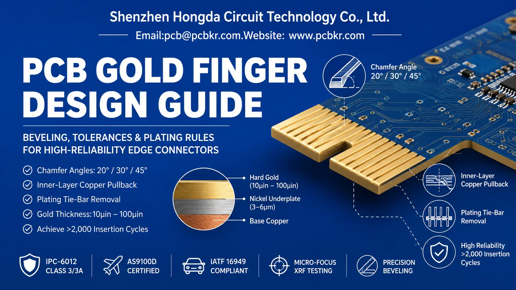
PCB Gold Finger Design Guide: Beveling, Tolerances & Plating Rules for High-Reliability Edge Connectors
PCB Gold Finger serves as the core conductive and mechanical contact component of printed circuit board edge connectors, acting as the definitive electrical and mechanical bridge that links a daughter card to its host system in hardware design. In the engineering specification workflow of hardware engineers, the design and validation of PCB gold fingers are critical priority items that determine the overall stability and service life of board-level interconnection systems, covering diversified high-end application scenarios including PCIe Gen 5 accelerator slots, industrial backplanes transmitting 224G PAM4 high-speed signals, and automotive ECU systems that strictly comply with ISO 26262 functional safety mandates.
As the key contact interface for signal transmission and power conduction between circuit boards, the manufacturing quality and structural precision of PCB gold fingers directly dictate system operational reliability. Substandard PCB gold fingers, typically caused by insufficient gold plating thickness, unqualified plating uniformity, missing edge chamfer processing, or surface oxidation and contamination, will not only lead to poor contact, signal attenuation, intermittent circuit conduction and other local board-level problems. More critically, these subtle manufacturing defects will trigger cascading system-level failures in complex working conditions such as high-speed signal transmission, long-term vibration, and high and low temperature cycling.
In mass industrial production and commercial application scenarios, the hidden dangers brought by defective PCB gold fingers are extremely costly. Minor quality flaws will cause equipment operation abnormalities and functional failures, while batch unqualified gold finger products will further lead to large-scale field equipment recalls, bringing millions of dollars in economic losses to enterprises, and also damaging product credibility and brand reputation. Therefore, in the hardware design and PCB manufacturing verification process, engineers must strictly standardize the plating process, dimensional tolerance and chamfer structure of gold fingers, and implement rigorous quality testing to eliminate hidden risks of system failure from the source.
This guide is written for procurement professionals and PCB layout designers who need to understand the manufacturing physics behind PCB gold fingers. We cover chamfer angles, inner-layer pullback distances, plating tie-bar removal protocols, and the process controls that separate commodity fabricators from suppliers capable of delivering >2,000 insertion cycles.
What Are PCB Gold Fingers? Anatomy of the Edge Connector Interface
A PCB gold finger—also called an edge connector pad or electroplated gold contact—is a selective hard gold deposit running along the board edge. Unlike ENIG, a chemical immersion finish optimized for solderability, hard gold is an electrolytic alloy (typically 99.7% gold with cobalt or nickel) engineered specifically for mechanical wear resistance and stable contact resistance under repeated mating cycles.
The Copper-Nickel-Gold Stackup
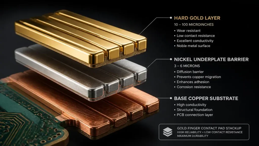
PCB Gold Finger Stackup Diagram: Hard Gold, Nickel, and Copper Layers
The functional stack begins with base copper, followed by a nickel underlayer typically 3–6 μm thick, and capped with hard gold. The nickel barrier prevents copper diffusion into the gold layer—which would create brittle intermetallics—and provides a hard substrate supporting the gold during mechanical wiping. Gold thickness is dictated by insertion cycle requirements. For a PCIe card-edge interface expected to survive 500+ hot-swaps, IPC-4552 recommends a minimum of 0.8 μm (≈31 μin) hard gold. For industrial line cards targeting >2,000 cycles, 1.27–2.54 μm (50–100 μin) is the pragmatic specification.
Why Hard Gold Outperforms ENIG on Edge Connectors
ENIG deposits only 0.05–0.1 μm of soft, pure gold. That protects nickel from oxidation during storage, but wears through rapidly under connector spring pressure. Once compromised, the exposed nickel exhibits higher contact resistance and is susceptible to fretting corrosion in vibration environments. Hard gold, alloyed to 130–200 HK hardness and deposited electrolytically to controlled thicknesses, maintains low, stable resistance across thousands of mating cycles—a non-negotiable requirement for server backplanes, telecom line cards, and medical device interfaces.
Gold Finger Chamfer Angle Specifications: 20°, 30°, and 45° Beveling Explained
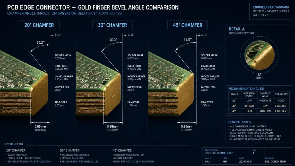
PCB Gold Finger Chamfer Angles Comparison (20° vs 30° vs 45°)
PCB gold finger chamfering—also referred to as edge beveling or connector ramp profiling—is a CNC grinding operation that transforms the sharp 90° board edge into an angled insertion ramp. Without this bevel, the leading edge can damage connector pins, scrape off gold plating, or cause misalignment in high-density card-edge slots.
Standard 30° Chamfer for PCIe and Consumer Card-Edge Interfaces
The 30-degree gold finger chamfer is the most commonly specified angle across consumer electronics, computing, and networking hardware. It provides a balanced compromise between insertion smoothness and board edge retention. At Shenzhen Hongda Circuit Technology Co., Ltd., 30° bevels are machined on Schmoll MX-500 profile routers with ±2° angular accuracy and 0.5–1.5 mm chamfer depth, followed by edge polishing to eliminate fiber exposure. For procurement teams auditing suppliers, verify that the fabricator measures chamfer angle with optical gauges rather than relying on tool offsets alone—angle drift during batch production is a common source of insertion force variation.
45° Heavy-Duty Beveling for Industrial and Automotive Edge Connectors
A 45-degree edge connector chamfer is specified when the board is thick (>2.4 mm), the connector housing has limited lead-in geometry, or the application involves high-insertion-force industrial connectors. The steeper angle creates a longer ramp, reducing peak insertion force and minimizing plating damage during aggressive mating. Automotive ECU interfaces and railway control modules frequently use 45° bevels combined with 1.0–1.5 mm depth to accommodate vibration-induced misalignment.
20° Minimal Chamfer for Space-Constrained Memory Modules
In ultra-compact designs—such as DDR5 memory modules or mini-PCIe cards—a 20-degree gold finger bevel provides just enough insertion assistance without consuming excessive edge length. The trade-off is higher sensitivity to board edge straightness; any bow or twist amplifies insertion force because the shallow ramp offers less mechanical advantage. If your design uses 20° chamfers, specify tighter board flatness controls (≤0.75% per IPC-6012) and confirm that your supplier supports selective multi-angle beveling in a single setup.
Chamfer Depth Tolerances and Burr-Free Requirements
Regardless of angle, the chamfer depth must maintain a smooth transition across the plated edge. Burrs, fiber pull-out, or nickel-gold creep onto the sidewall create debris that contaminates the mating connector. A robust DFM specification should state: “Chamfer depth 0.5–1.5 mm, burr-free, no fiber exposure, plating integrity verified under 10× magnification.” At Hongda, boards undergo secondary edge polishing after routing to meet this standard, particularly for medical and aerospace programs where zero particle generation is mandatory.
Inner-Layer Copper Pullback and Solder Mask Clearance Near Board Edge
The area immediately adjacent to a gold finger is a high-stress zone. Repeated insertion forces transmit through the gold-nickel stack into the laminate, creating a propagation path for microcracks if inner-layer copper extends too close to the board edge.
Preventing Delamination Under Repeated Insertion Stress
For high-insertion-cycle designs, inner-layer copper should be pulled back from the rout edge by a minimum distance scaling with board thickness—typically 0.5 mm for 1.6 mm boards and 0.8 mm for 3.2 mm boards. This clearance prevents the copper-to-resin interface from acting as a crack initiation site. Additionally, specifying high-Tg laminate (≥170°C) reduces CTE mismatch between the FR-4 core and the metal stackup during reflow. For boards >3.2 mm thick, an unfilled fiberglass edge band (0.5 mm) absorbs insertion shock and prevents z-axis delamination.
Solder Mask Registration Accuracy for Gold Finger Exposures
Solder mask must expose the full contact pad while preventing mask bleed onto the mating surface. A mask pullback of 0.1 mm minimum from the gold finger edge is standard, but achieving this consistently requires LDI (laser direct imaging) registration. Hongda’s SCREEN Ledia LDI systems hold ±10 μm solder mask registration, critical when finger pitch shrinks below 1.0 mm. Procurement tip: ask your supplier whether they use LDI or traditional photo-tool exposure for mask imaging. On fine-pitch edge connectors, photo-tool stretch and misregistration can mask over the finger edge or expose adjacent circuitry—both are yield killers.
Plating Tie-Bars, Bus Bars, and DFM-Critical Removal Protocols
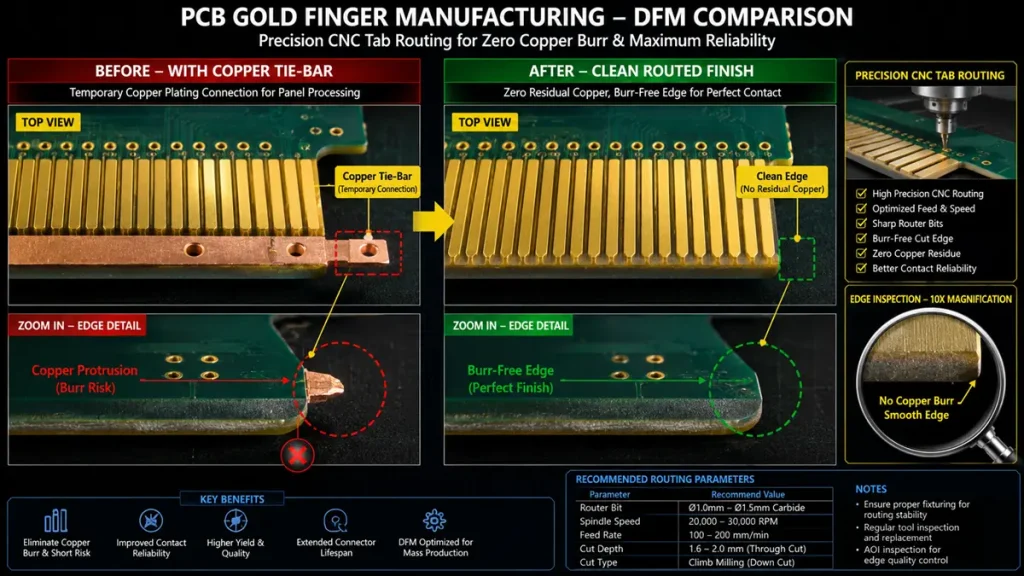
PCB Gold Finger Tie-Bar Removal DFM: Before vs After CNC Routing
Hard gold is electrolytic. Current must reach every finger pad, which means temporary copper connections—plating tie-bars or plating bus bars—must link the fingers to the panel edge during deposition. These tie-bars are subsequently removed, but their design and removal method directly impact final board quality.
Why Electroplated Gold Requires Temporary Current Distribution Networks
A tie-bar width of 0.5–1.0 mm is necessary to prevent current crowding, which causes thickness variation across the finger row. Thickness variation >10% between fingers creates uneven contact resistance and accelerates wear on thinner deposits. The tie-bar should connect at the finger root (board-edge side) to minimize post-removal cleanup, and it must be located outside the final board outline.
Tab Routing vs. V-Scoring for Clean Tie-Bar Separation
After plating, tie-bars are removed by CNC routing or V-scoring. Routing is preferred for clean edges; V-scoring is cheaper but risks fracturing the beveled edge on thick boards. For medical and aerospace applications requiring absolute zero residual copper, tab routing with mouse-bite breakaway ensures the tie-bar breaks flush with the board edge. Any residual tie-bar material beyond 0.0 mm protrusion creates a short risk between adjacent fingers and can interfere with connector polarization keys.
Residual Copper Risks and Connector Shorting Hazards
The most common field failure mode from poor tie-bar removal is intermittent shorting between adjacent fingers. When a 0.1 mm sliver of copper remains, it bridges contacts under mechanical vibration or humidity. During incoming inspection, demand edge photographs at 40× magnification showing the tie-bar removal zone. If the fabricator cannot produce these images from their standard process, that indicates manual cleanup rather than CNC-controlled removal.
Achieving >2,000 Insertion Cycles: Gold Thickness, Nickel Underplate, and Surface Integrity
Mating life is the product of gold thickness, nickel quality, surface finish, and connector design. For procurement teams evaluating suppliers against high-cycle requirements, the following metrics are non-negotiable.
Hard Gold Thickness Ranges from 10 μin to 100 μin
Low-cycle prototypes may use 10–15 μin (0.25–0.38 μm) hard gold. Production edge connectors in servers and telecom equipment typically specify 30–50 μin (0.76–1.27 μm). For extreme-cycle applications—test fixtures, military backplanes, or industrial hot-swap modules—80–100 μin (2.03–2.54 μm) provides the wear margin necessary to survive >2,000 insertions. The cost delta between 30 μin and 100 μin is significant due to gold consumption, so selective plating (confining hard gold to the finger area only) is essential for cost control.
The Nickel Underplate as a Diffusion Barrier
Nickel underplate quality is often overlooked but equally critical as gold thickness. A porous or contaminated nickel layer allows copper diffusion even under thick gold, leading to contact resistance drift. Specify a minimum nickel thickness of 3 μm with sulfur-free chemistry, and require microsection analysis showing continuous nickel coverage without voids at the copper interface.
XRF Verification and In-Process Thickness Monitoring
Thickness cannot be validated by appearance. Hongda uses 50 μm micro-focus XRF (X-ray fluorescence) to verify gold and nickel thickness on every production panel, with data logged for traceability. For Class 3 and aerospace work, demand XRF spot readings on every finger row, not just coupon areas. Coupon readings average across multiple fingers and can hide localized thin spots caused by current density variation in the plating bath.
Procurement Decision Framework: Evaluating Gold Finger PCB Suppliers in 2026
Selecting a gold finger PCB manufacturer requires moving beyond price-per-square-centimeter and auditing the processes that determine insertion-cycle reliability.
Certifications That Matter: IPC-6012 Class 3, AS9100D, and IATF 16949
For industrial, medical, and automotive edge connectors, IPC-6012 Class 3 is the baseline. Aerospace programs require AS9100D. Automotive ECU interfaces increasingly demand IATF 16949 with full PPAP capability. A supplier holding these certifications has demonstrated sustained process control, but certification alone does not guarantee gold finger expertise. Ask specifically how many hard gold panels they process monthly and what their plating bath turnover rate is—stagnant baths accumulate organic contaminants that degrade nickel underplate adhesion.
Equipment Audit Checklist for Selective Hard Gold Lines
Dedicated hard gold lines separate serious suppliers from generalists. Shared ENIG/hard gold lines introduce cross-contamination risk and thickness control drift. Key equipment to verify:
- LDI imaging (±10 μm registration) for solder mask and plating resist accuracy
- CNC chamfering with angle verification, not manual grinding
- Micro-focus XRF (≤50 μm spot size) for in-process thickness monitoring
- 3D X-Ray (AXI) for inner-layer alignment verification on high-layer-count boards
- Profile routers with ±0.025 mm accuracy for tie-bar removal
Hongda’s 2026 equipment lineup includes SCREEN Ledia LDI, Mitsubishi laser drilling, Nordson DAGE X-Ray inspection, and Schmoll MX-500 routing systems—an investment profile consistent with high-reliability gold finger production.
DFM Review Turnaround and First-Article Yield Expectations
A supplier’s DFM review speed correlates with their engineering depth. If a fabricator takes three days to flag a tie-bar placement issue, that indicates reactive engineering rather than proactive design partnership. Target a 24-hour DFM turnaround for gold finger designs, with first-article yield >95% on straightforward 30° chamfer, 50 μin gold specifications. Yield below 90% on standard geometries suggests process instability in plating or beveling.
Frequently Asked Questions About Gold Finger PCB Manufacturing
What is the difference between hard gold and ENIG for edge connectors?
Hard gold is an electrolytic alloy (99.7% gold with cobalt/nickel) deposited to 10–100 μin thickness, engineered for mechanical wear resistance and >1,000 insertion cycles. ENIG is a chemical immersion finish with only 0.05–0.1 μm of soft pure gold, optimized for solderability but unsuitable for repeated mechanical contact. For production edge connectors, hard gold is the only finish that guarantees stable contact resistance across the product lifecycle.
How do I specify chamfer angle and depth on my fabrication drawing?
State the angle (20°, 30°, or 45°), depth (0.5–1.5 mm), and tolerance (±2°) in the fabrication notes and on the mechanical layer. For boards with gold fingers on multiple edges, specify selective chamfering requirements. Include a note requiring burr-free edges with no fiber exposure, verified under 10× magnification. If your design uses tab routing for depaneling, explicitly state this to avoid V-scoring that can fracture the bevel.
Why do gold fingers need plating tie-bars, and how are they removed?
Tie-bars are temporary copper connections that conduct plating current to each finger during electrolytic hard gold deposition. They are removed after plating by CNC routing or tab breakaway. Residual copper must be 0.0 mm beyond the board edge to prevent shorting between fingers or interference with connector polarization keys. Always verify tie-bar removal with edge photographs at 40× magnification during incoming inspection.
What gold thickness do I need for 2,000+ insertion cycles?
For >2,000 cycles, specify 80–100 μin (2.03–2.54 μm) hard gold over a minimum 3 μm nickel underplate. This thickness provides sufficient wear margin to prevent nickel exposure even under high-insertion-force connectors. Combine this with high-Tg laminate and inner-layer copper pullback from the board edge to prevent delamination. Verify thickness with micro-focus XRF on actual fingers, not just test coupons
How do I audit a PCB supplier’s gold finger capability before placing production orders?
Request certification scope (IPC-6012 Class 3/3A, AS9100D, IATF 16949), equipment list (dedicated hard gold line, CNC chamfering, micro-focus XRF), and process data from recent gold finger builds. Ask for DFM examples showing how they handle tie-bar placement, solder mask pullback, and inner-layer clearance. A capable supplier will return a DFM review within 24 hours and provide first-article inspection reports including XRF thickness maps and edge photographs.
Specifying Gold Fingers That Survive Real-World Insertion Cycles
PCB gold finger design is a multi-parameter optimization problem. The chamfer angle determines insertion force. The inner-layer pullback prevents delamination. The tie-bar design and removal method eliminate field shorting risks. The gold thickness and nickel underplate quality dictate how many times the connector can be mated before contact resistance degrades. Each parameter is measurable, auditable, and controllable—if your supplier has invested in the right equipment and process discipline.
For procurement professionals evaluating edge connector PCB suppliers in 2026, the decisive factors are not price alone, but the presence of dedicated selective hard gold lines, CNC chamfering with optical angle verification, micro-focus XRF thickness monitoring, and engineering teams that can return DFM feedback within 24 hours. Shenzhen Hongda Circuit Technology Co., Ltd. operates these capabilities under IPC-6012 Class 3/3A and AS9100D certification, with selective hard gold plating from 10 μin to 100 μin and precision beveling held to ±2° tolerance. For technical consultation or DFM review, contact sales@pcbkr.com.
About Author
David Chen https://www.linkedin.com/in/pcbcoming
David Chen boasts an extensive professional background in PCBA manufacturing, PCBA testing, and PCBA optimization, with specialized expertise in high-precision PCBA fault analysis and rigorous PCBA reliability testing. The author has worked with high-layer-count server PCB fabrication, ultra-low-loss backplane stackups, and thermo-mechanical reliability optimization for AI infrastructure projects involving 112G and 224G PAM4 architectures. Skilled in complex circuit design and cutting-edge advanced PCB manufacturing processes, he delivers solutions that elevate product durability and performance across industrial applications. His technical articles focusing on PCBA manufacturing workflows and testing methodologies are widely cited by industry peers, research institutions, and technical platforms, solidifying his reputation as a recognized technical authority in the global circuit board manufacturing sector.